

Page 1

HD151011
Dual BCD Programmable Counter
with Synchronous Preset Enable
ADE-205-100(Z)
Rev 0
April 1995
The HD151011 has BCD decimal two digits down counter and D-type Flip Flop. The counter can set up to
max 99 counts and synchronous preset ( SPE) input can preset the data. When the count value is 0, the next
clock pulse presets the data to invert the output. D-type Flip Flop takes the counter output as clock pulse,
whose data is transferred to output at the rise edge. It is applied to generate AC signal for STN type liquid
crystal and general-use divider.
Features
• High speed operation
tpd (CLK or CLK to Q) = 35 ns (typ)
• High output current
Fanout of 10 LS TTL Loads
• Wide operating voltage
Vcc = 2 to 6 V
• Low supply current (Ta = 25°C)
Icc (Static) = 4 µA (max)
Page 2

HD151011
Function Table
Control Inputs
CLR PR SPE C/T Mode Operation Description
HHHXGenerally count Down count at the rise edge of clock (CLK),
Down count at the fall edge of clock (CLK)
X X L X Synchronous preset Jn data is preset at the rise of clock (CLK),
the fall of clock (CLK)
———H — Clock inputs (CLK, CLK) is CMOS level
———L — Clock inputs (CLK, CLK) is TTL level
L H — — Initialize of Q output Initialize of Q = "L"
H L — — Initialize of Q output Initialize of Q = "H"
H: High level
L: Low level
Z: Immaterial
—: Irrespective of condition
1. Synchronous preset (SPE) input can set max 99 down counts.
2. When the count value is 0, the next clock pulse presets the data to invert the output.
3. CLR and PR inputs initialize output state.
4. Clock inputs (CLK, CLK) is selectable CMOS level (V
(Jn, C/T, PR, CLR and SPE inputs are CMOS level)
Note: Don't set data exceeding 99 to Jn. (J0: LSB, J7: MSB)
= 2.0 to 6.0 V) and TTL level (VCC = 4.5 to 5.5V)
CC
2
Page 3
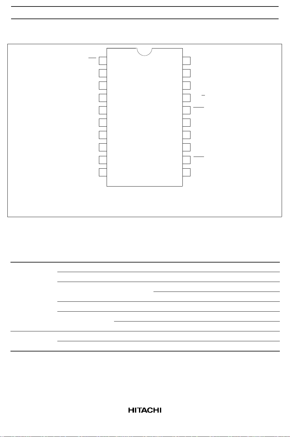
Pin Arrangement
HD151011
1
CO
2
J 0
3
J 1
J 2
4
J 3
5
J 4
6
J 5
7
J 6
8
9
J 7
10
GND
(Top view)
* Pins 18 and 19 are for function test only and should be open.
20
19
18
17
16
15
14
13
12
11
V
CC
(Test 1)*
(Test 2)*
C / T
CLK
CLK
Q
PR
SPE
CLR
Pin Description
Pin Name Pin Description
Input pins J0 to J7 Count data input for option
C/T Level change input for CLK, CLK (CMOS level or TTL level)
CLK, CLK Clock inputs CLK : Rise edge trigger
CLK : Fall edge trigger
SPE Preset input for Jn data
PR Preset input for D-type Flip Flop (Initialize "L" at Q output)
CLR Clear input for D-type Flip Flop (Initialize "H" at Q output)
Output pins CO Output for BCD decimal counter
Q Output for D-type Flip Flop
3
Page 4
HD151011
Absolute Maximum Ratings
Item Symbol Ratings Unit
Supply voltage V
Input / output voltage VIN / V
VCC, GND current ICC, I
Output current / pin I
Power dissipation P
CC
OUT
GND
OUT
T
Storage temperature Tstg –65 to 150 °C
Input diode current I
Output diode current I
IK
OK
Notes: 1. The absolute maximum ratings are values which must not individually be exceeded, and
furthermore, no two of which may be realized at the same time.
2. All voltage values except for differential input voltage are with respect to network ground
terminal.
Recommended Operating Conditions
–0.5 to 7.0 V
–0.5 to VCC +0.5 V
±50 mA
±25 mA
757 mW
±20 mA
±20 mA
Item Symbol Min Typ Max Unit
Supply voltage V
CC
Input / output voltage VIN /
OUT
2—6V
0—VCCV
Operating temperature Topr –40 — +85 °C
Input rise / fall time
*1
VCC = 2.5 V tr, tf 0 — 1000 ns
VCC = 4.5 V 0 — 500
VCC = 5.5 V 0 — 400
Note: 1. This item guarantees maximum limit when one input switches.
4
Page 5
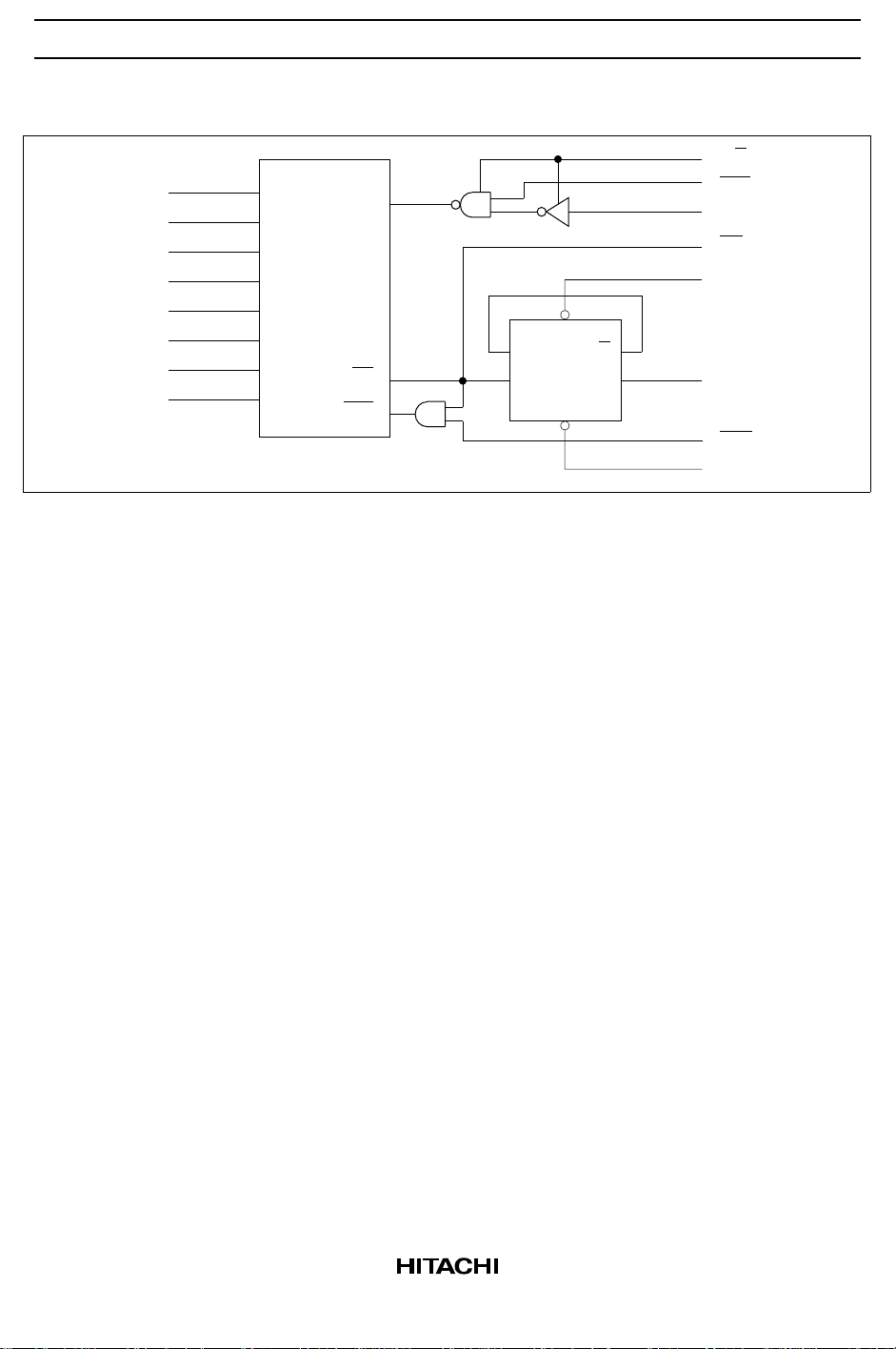
Logic Diagram
J0 J0
J1 J1
J2 J2
J3 J3
J4 J4
J5 J5
J6 J6
J7 J7
CLK
BCD decimal counter
CO
SPE
D
CK
PR
CLR
HD151011
C/T
CLK
CLK
CO
PR
Q
Q
Q
SPE
CLR
5
Page 6

HD151011
A
Electrical Characteristics
Ta = 25°C Ta = –40 to 85°C
Item Symbol V
High level input V
IH
2.0 1.5 — — 1.5 — V J0 to J7
voltage 4.5 3.15 — — 3.15 — C/T, SPE
6.0 4.2 — — 4.2 — PR, CLR
2.0 1.5 — — 1.5 — CLK, CLK C/T = V
4.5 3.15 — — 3.15 —
6.0 4.2 — — 4.2 —
4.5 to
5.5
Low level input V
IL
2.0 — — 0.5 — 0.5 V J0 to J7
voltage 4.5 — — 1.35 — 1.35 C/T, SPE
6.0 — — 1.8 — 1.8 PR, CLR
2.0 — — 0.5 — 0.5 CLK, CLK C/T = V
4.5 — — 1.35 — 1.35
6.0 — — 1.8 — 1.8
4.5 to
5.5
High level output
V
OH
2.0 1.9 2.0 — 1.9 — V VIN =
voltage
4.5 4.4 4.5 — 4.4 —
6.0 5.9 6.0 — 5.9 —
4.5 4.18 4.31 — 4.13 — IOH = –4 mA
6.0 5.68 5.80 — 5.63 — IOH = –5.2 m
Low level output
V
OL
2.0 — 0.0 0.1 — 0.1 V VIN =
voltage
4.5 — 0.0 0.1 — 0.1
6.0 — 0.0 0.1 — 0.1
4.5 — 0.17 0.26 — 0.33 IOL = 4 mA
6.0 — 0.18 0.26 — 0.33 IOL = 5.2 mA
Input capacitance IIN 6.0 — — ±0.1 — ±1.0 mA VIN = VCC or GND
Supply current I
CC
6.0 — — 4.0 — 40.0 mA VIN = VCC or GND
Min Typ Max Min Max Unit Test Conditions
CC
2.0 — — 2.0 — C/T = V
— — 0.8 — 0.8 C/T = V
V
or V
IH
V
or V
IH
IOH = –20 µA
IL
IOL = 20 µA
IL
IH
IL
IH
IL
6
Page 7

HD151011
Switching Characteristics (CL = 50 pF, tr = tf = 6 ns)
Ta = 25°C Ta = –40 to 85°C
Item Symbol V
Maximum clock
fmax 2.0 — — 4 — 3 MHz
frequency
4.5 — 36 20 — 16
6.0 — — 24 — 19
Output rise / fall time t
TLH
t
THL
2.0 — 30 75 — 95 ns
4.5 — 8 15 — 19
6.0 — 7 13 — 16
Propagation delay
t
PLH
2.0 — — 250 — 318 ns CLK or CLK to CO
time
t
PHL
4.5 — 30 50 — 63
6.0 — — 45 — 53
t
PLH
t
PHL
2.0 — — 300 — 380 CLK or CLK to Q
4.5 — 35 60 — 75
6.0 — — 53 — 65
t
PLH
t
PHL
2.0 — — 150 — 185 PR or CLR to Q
4.5 — 18 30 — 38
6.0 — — 25 — 32
Pulse width tw 2.0 80 — — 100 — ns
(CLK, CLK, PR, CLR) 4.5 16 — — 20 —
6.0 14 — — 17 —
Setup time ts 2.0 100 — — 125 — ns
(Jn - CLK, CLK) 4.5 20 — — 25 —
(SPE, CLK, CLK) 6.0 17 — — 21 —
Hold time th 2.0 15 — — 15 — ns
(Jn - CLK, CLK) 4.5 10 — — 10 —
(SPE, CLK, CLK) 6.0 5 — — 5 —
Input capacitance C
Power dissipation
IN
C
PD
— — 5 10 — 10 pF
——48———pF
capacitance
Note: 1. CPD is equivalent capacitance inside of the IC calculated from the operating current without load
(see test circuit). The average operating current without load is calculated according to the
expression below.
I
(opr) = CPD VCC • fIN + I
CC
Min Typ Max Min Max Unit Test Conditions
CC
CC
7
Page 8

HD151011
• Test Circuit
V
CC
Input
Pulse generator
Z = 50
out
Ω
Input
Pulse generator
Z = 50
out
Ω
See Function Table
Note: 1. CL includes probe and jig capacitance.
• Waveforms – 1
6 ns
10 %
t
w
CLK
CLK
t
w
6 ns
90 %
90 %
*1 *1
V
10 %
Q
10 %
V
ref
t
PLH
ref
90 %
50 %
t
TLH
t
PLH
J0
J1
J7
C/T
CLK
CLK
SPE
PR
CLR
V
CC
Output
Q
Output
CO
C
L
C
L
*1
V
IH
GND
t
PHL
V
90 %
50 %
10 %
t
THL
t
PHL
OH
V
OL
90 %
CO
10 %
50 %
t
TLH
Note: 1. In case of C/T = "L", CLK, CLK is VIH = 3 V, Vref is 1.3 V
In case of C/T = "H", CLK, CLK is VIH = VCC, Vref is VCC × 50%
8
90 %
50 %
10 %
t
THL
V
OH
V
OL
Page 9

• Waveforms – 2
6 ns
90 %
Jn
10 %
CLK
CLK
*2
F/F Output
Notes: 1. In case of C/T = "L", CLK, CLK is VIH = 3 V, Vref is 1.3 V
In case of C/T = "H", CLK, CLK is VIH = VCC, Vref is VCC × 50%
2. F/F output is internal signal of IC.
90 %
50 %
10 %
t
s
10 %
V
ref
90 %
*1
10 %
6 ns
Internal delay
50 %
HD151011
V
CC
GND
*1
V
IH
GND
V
OH
V
OL
• Waveforms – 3
90 %
Jn
10 %
t
h
CLK
CLK
*2
10 %
F/F Output
Notes: 1. In case of C/T = "L", CLK, CLK is VIH = 3 V, Vref is 1.3 V
In case of C/T = "H", CLK, CLK is VIH = VCC, Vref is VCC × 50%
2. F/F output is internal signal of IC.
V
ref
90 %
*1
10 %
6 ns
Internal delay
90 %
50 %
10 %
50 %
6 ns
V
CC
GND
V
IH
GND
V
OH
V
OL
*1
9
Page 10

HD151011
• Waveforms – 4
6 ns
90 %
SPE
10 %
CLK
CLK
*2
F/F Output
Notes: 1. In case of C/T = "L", CLK, CLK is VIH = 3 V, Vref is 1.3 V
In case of C/T = "H", CLK, CLK is VIH = VCC, Vref is VCC × 50%
2. F/F output is internal signal of IC.
90 %
50 %
10 %
t
s
10 %
V
ref
90 %
*1
10 %
6 ns
Internal delay
50 %
V
CC
GND
V
IH
GND
V
OH
V
OL
*1
• Waveforms – 5
90 %
SPE
10 %
t
h
CLK
CLK
*2
10 %
F/F Output
Notes: 1. In case of C/T = "L", CLK, CLK is VIH = 3 V, Vref is 1.3 V
In case of C/T = "H", CLK, CLK is VIH = VCC, Vref is VCC × 50%
2. F/F output is internal signal of IC.
V
ref
90 %
*1
10 %
6 ns
Internal delay
90 %
50 %
10 %
50 %
6 ns
V
CC
GND
V
IH
GND
V
OH
V
OL
*1
10
Page 11

• Waveforms – 6
HD151011
CLR
PR
t
f
90 %
50 %
10 %
t
w
t
PHL
Q
50 %
50 %
10 %
t
90 %
r
V
CC
GND
90 %
50 %
10 %
t
t
PLH
f
t
w
50 %
50 %
10 %
t
90 %
r
V
CC
GND
V
OH
V
OL
11
Page 12

HD151011
Timing Chart
CLK
SPE
J0
J1
J2
J3
J4
J5
J6
J7
(CO=SPE)
CLR
(Initialize of CLR)
Q
PR
(Initialize of PR)
Q
Count 54321032102322
12
Page 13

Example of Application Circuit
• AC Signal Generator for STN Type Liquid Crystal Panel
CLK (CLK) : CMOS level input
Initialize counter : 32
HD151011
CO
J 0
J 1
J 2
J 3
J 4
J 5
J 6
J 7
GND
*When initializing output D-F/F apply "L"
V
CC
(Test 1)
(Test 2)
C/T
CLK
CLK
PR
SPE
CLR
NC
NC
Q
*
*
13
Page 14

HD151011
Timing Chart
• Example of AC Signal Generator
1 2 3 31 32 33 34 35 65 66 67 68
CLK
SPE
J0
J1
1digit=2
J2
J3
2digits=3
(CO=SPE)
J4
J5
J6
J7
CLR
Q
PR
Q
14
Count
32 31 30 2 1 0 32 31 1 0 32 31
Page 15

Package Dimensions
6.80 Max
20 11
110
+0.08
0.22
–0.07
0.20 ± 0.06
6.50
0.13
0.65 Max
0.65
HD151011
Unit : mm
Unit: mm
4.40
1.0
M
6.40 ± 0.20
0.10
1.10 Max
Dimension including the plating thickness
Base material dimension
0.17 ± 0.05
0.15 ± 0.04
+0.03
–0.04
0.07
0° – 8°
Hitachi Code
JEDEC
EIAJ
Weight
(reference value)
0.50 ± 0.10
TTP-20DA
—
—
0.07 g
15
Page 16

Cautions
1. Hitachi neither warrants nor grants licenses of any rights of Hitachi’s or any third party’s patent,
copyright, trademark, or other intellectual property rights for information contained in this document.
Hitachi bears no responsibility for problems that may arise with third party’s rights, including
intellectual property rights, in connection with use of the information contained in this document.
2. Products and product specifications may be subject to change without notice. Confirm that you have
received the latest product standards or specifications before final design, purchase or use.
3. Hitachi makes every attempt to ensure that its products are of high quality and reliability. However,
contact Hitachi’s sales office before using the product in an application that demands especially high
quality and reliability or where its failure or malfunction may directly threaten human life or cause risk
of bodily injury, such as aerospace, aeronautics, nuclear power, combustion control, transportation,
traffic, safety equipment or medical equipment for life support.
4. Design your application so that the product is used within the ranges guaranteed by Hitachi particularly
for maximum rating, operating supply voltage range, heat radiation characteristics, installation
conditions and other characteristics. Hitachi bears no responsibility for failure or damage when used
beyond the guaranteed ranges. Even within the guaranteed ranges, consider normally foreseeable
failure rates or failure modes in semiconductor devices and employ systemic measures such as failsafes, so that the equipment incorporating Hitachi product does not cause bodily injury, fire or other
consequential damage due to operation of the Hitachi product.
5. This product is not designed to be radiation resistant.
6. No one is permitted to reproduce or duplicate, in any form, the whole or part of this document without
written approval from Hitachi.
7. Contact Hitachi’s sales office for any questions regarding this document or Hitachi semiconductor
products.
Hitachi, Ltd.
Semiconductor & Integrated Circuits.
Nippon Bldg., 2-6-2, Ohte-machi, Chiyoda-ku, Tokyo 100-0004, Japan
Tel: Tokyo (03) 3270-2111 Fax: (03) 3270-5109
URL NorthAmerica : http:semiconductor.hitachi.com/
For further information write to:
Hitachi Semiconductor
(America) Inc.
179 East Tasman Drive,
San Jose,CA 95134
Tel: <1> (408) 433-1990
Fax: <1>(408) 433-0223
Europe : http://www.hitachi-eu.com/hel/ecg
Asia (Singapore) : http://www.has.hitachi.com.sg/grp3/sicd/index.htm
Asia (Taiwan) : http://www.hitachi.com.tw/E/Product/SICD_Frame.htm
Asia (HongKong) : http://www.hitachi.com.hk/eng/bo/grp3/index.htm
Japan : http://www.hitachi.co.jp/Sicd/indx.htm
Hitachi Europe GmbH
Electronic components Group
Dornacher Stra§e 3
D-85622 Feldkirchen, Munich
Germany
Tel: <49> (89) 9 9180-0
Fax: <49> (89) 9 29 30 00
Hitachi Europe Ltd.
Electronic Components Group.
Whitebrook Park
Lower Cookham Road
Maidenhead
Berkshire SL6 8YA, United Kingdom
Tel: <44> (1628) 585000
Fax: <44> (1628) 778322
Hitachi Asia Pte. Ltd.
16 Collyer Quay #20-00
Hitachi Tower
Singapore 049318
Tel: 535-2100
Fax: 535-1533
Hitachi Asia Ltd.
Taipei Branch Office
3F, Hung Kuo Building. No.167,
Tun-Hwa North Road, Taipei (105)
Tel: <886> (2) 2718-3666
Fax: <886> (2) 2718-8180
Copyright ' Hitachi, Ltd., 1999. All rights reserved. Printed in Japan.
Hitachi Asia (Hong Kong) Ltd.
Group III (Electronic Components)
7/F., North Tower, World Finance Centre,
Harbour City, Canton Road, Tsim Sha Tsui,
Kowloon, Hong Kong
Tel: <852> (2) 735 9218
Fax: <852> (2) 730 0281
Telex: 40815 HITEC HX
 Loading...