

Page 1
1
2
3
4
8
7
6
5
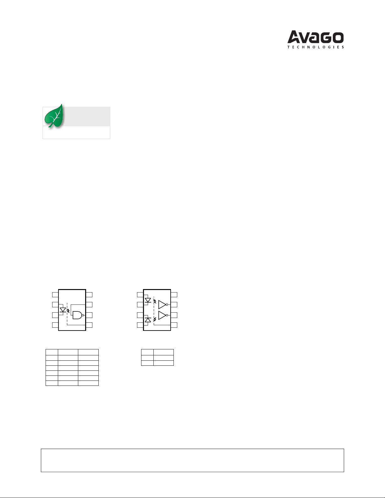
CATHODE
ANODE
GND
V
V
CC
O
1
2
3
4
8
7
6
5
ANODE
2
CATHODE
2
CATHODE
1
ANODE
1
GND
V
V
CC
O2
V
E
V
O1
6N137, HCPL-2601/2611
HCPL-0600/0601/0611
HCPL-2630/2631/4661
HCPL-0630/0631/0661
NC
NC
LED
ON
OFF
ON
OFF
ON
OFF
ENABLE
H
H
L
L
NC
NC
OUTPUT
L
H
H
H
L
H
TRUTH TABLE
(POSITIVE LOGIC)
LED
ON
OFF
OUTPUT
L
H
TRUTH TABLE
(POSITIVE LOGIC)
SHIELD SHIELD
6N137, HCNW137, HCNW2601, HCNW2611, HCPL-0600,
HCPL-0601, HCPL-0611, HCPL-0630, HCPL-0631, HCPL-0661,
HCPL-2601, HCPL-2611, HCPL-2630, HCPL-2631, HCPL-4661
High CMR, High Speed TTL Compatible Optocouplers
Data Sheet
Lead (Pb) Free
RoHS 6 fully
compliant
RoHS 6 fully compliant options available;
-xxxE denotes a lead-free product
Description
The 6N137, HCPL-26XX/06XX/4661, HCNW137/26X1 are
optically coupled gates that combine a GaAsP light emitting diode and an integrated high gain photo detector.
An enable input allows the detector to be strobed. The
output of the detector IC is an open collector Schottkyclamped transistor. The internal shield provides a guaranteed common mode transient immunity speci cation
up to 15,000 V/µs at Vcm=1000V.
This unique design provides maximum ac and dc circuit isolation while achieving TTL compatibility. The optocoupler
ac and dc operational param e ters are guaranteed from 40°C to +85°C allowing troublefree system performance.
Functional Diagram
A 0.1 F bypass capacitor must be connected between pins 5 and 8.
Features
15 kV/µs minimum Common Mode Rejection (CMR)
at VCM = 1KV for HCNW2611, HCPL-2611, HCPL-4661,
HCPL-0611, HCPL-0661
High speed: 10 MBd typical
LSTTL/TTL compatible
Low input current capability: 5 mA
Guaranteed ac and dc performance over temper ature:
-40°C to +85°C
Available in 8-Pin DIP, SOIC-8, widebody packages
Strobable output (single channel products only)
Safety approval
UL recognized - 3750 V rms for 1 minute and 5000
Vrms* for 1 minute per UL1577 CSA approved
IEC/EN/DIN EN 60747-5-2 approved with
V
V
V
= 560 V
IORM
= 630 V
IORM
= 1414 V
IORM
for 06xx Option 060
peak
for 6N137/26xx Option 060
peak
for HCNW137/26X1
peak
MIL-PRF-38534 hermetic version available
(HCPL-56XX/66XX)
Applications
Isolated line receiver
Computer-peripheral interfaces
Microprocessor system interfaces
Digital isolation for A/D, D/A conversion
Switching power supply
Instrument input/output isolation
Ground loop elimination
Pulse transformer replacement
Power transistor isolation in motor drives
Isolation of high speed logic systems
*5000 V rms/1 Minute rating is for HCNW137/26X1 and Option 020
(6N137, HCPL-2601/11/30/31, HCPL-4661) products only.
CAUTION: It is advised that normal static precautions be taken in handling and assembly
of this component to prevent damage and/or degradation which may be induced by ESD.
Page 2

The 6N137, HCPL-26XX, HCPL-06XX, HCPL-4661, HCNW137,
and HCNW26X1 are suitable for high speed logic interfacing, input/output bu ering, as line receivers in environments that conventional line receivers cannot tolerate
and are recom mended for use in extremely high ground
or induced noise environments.
Selection Guide
Widebody
Minimum CMR 8-Pin DIP (300 Mil) Small-Outline SO-8 (400 Mil) Hermetic
Input Single
On- Single Dual Single Dual Single and Dual
dV/dt VCM Current Output Channel Channel Channel Channel Channel Channel
(V/μs) (V) (mA) Enable Package Package Package Package Package Packages
1000 10 5 YES 6N137
5,000 1,000 5 YES HCPL-0600 HCNW137
NO HCPL-2630 HCPL-0630
10,000 1,000 YES HCPL-2601 HCPL-0601 HCNW2601
NO HCPL-2631 HCPL-0631
15,000 1,000 YES HCPL-2611 HCPL-0611 HCNW2611
NO HCPL-4661 HCPL-0661
1,000 50 YES HCPL-2602
3, 500 300 YES HCPL-2612
1,000 50 3 YES HCPL-261A
NO HCPL-263A
[2]
1,000
1,000 YES HCPL-261N
NO HCPL-263N
1,000 50 12.5
[3]
HCPL-193X
HCPL-56XX
HCPL-66XX
[1]
[1]
[1]
HCPL-061A
[1]
HCPL-063A
[1]
HCPL-061N
[1]
HCPL-063N
[1]
[1]
[1]
[1]
[1]
[1]
[1]
Notes:
1. Technical data are on separate Avago publications.
2. 15 kV/µs with VCM = 1 kV can be achieved using Avago application circuit.
3. Enable is available for single channel products only, except for HCPL-193X devices.
2
Page 3

Ordering Information
HCPL-xxxx is UL Recognized with 3750 Vrms for 1 minute per UL1577.
HCNWxxxx is UL Rcognized with 5000 Vrms for 1 minute per UL1577.
Option
Part
Number
6N137
HCPL-2601
HCPL-2611
HCPL-2630
HCPL-2631
HCPL-4661
RoHS
Compliant
-000E No option
-300E #300 X X 50 per tube
-500E #500 X X X 1000 per reel
-020E #020 X 50 per tube
-320E #320 X X X 50 per tube
-520E #520 X X X X 1000 per reel
-060E #060 X 50 per tube
-560E -560 X X X X 1000 per reel
-000E No option
-300E #300 X X 50 per tube
-500E #500 X X X 1000 per reel
-020E #020 X 50 per tube
-320E #320 X X X 50 per tube
-520E #520 X X X X 1000 per reel
-060E #060 X 50 per tube
-360E - X X X 50 per tube
-000E No option
-300E #300 X X 50 per tube
-500E #500 X X X 1000 per reel
-020E #020 X 50 per tube
-320E #320 X X X 50 per tube
-520E #520 X X X X 1000 per reel
-060E #060 X 50 per tube
-360E #360 X X X 50 per tube
-560E #560 X X X X 1000 per reel
-000E No option
-300E #300 X X 50 per tube
-500E #500 X X X 1000 per reel
-020E #020 X 50 per tube
-320E #320 X X X 50 per tube
-520E -520 X X X X 1000 per reel
-000E No option
-300E #300 X X 50 per tube
-500E #500 X X X 1000 per reel
-020E #020 X 50 per tube
-320E #320 X X X 50 per tube
-520E #520 X X X X 1000 per reel
Non RoHS
Compliant
Package
300mil
DIP-8
300mil
DIP-8
300mil
DIP-8
300mil
DIP-8
300mil
DIP-8
Surface
Mount
Gull
Wing
Tape &
Reel
UL 5000 Vrms/
1 Minute
Rating
IEC/EN/DIN
EN 60747-5-2 Quantity
50 per tube
50 per tube
50 per tube
50 per tube
50 per tube
3
Page 4
SHIELD
8
6
5
2+
3
V
F
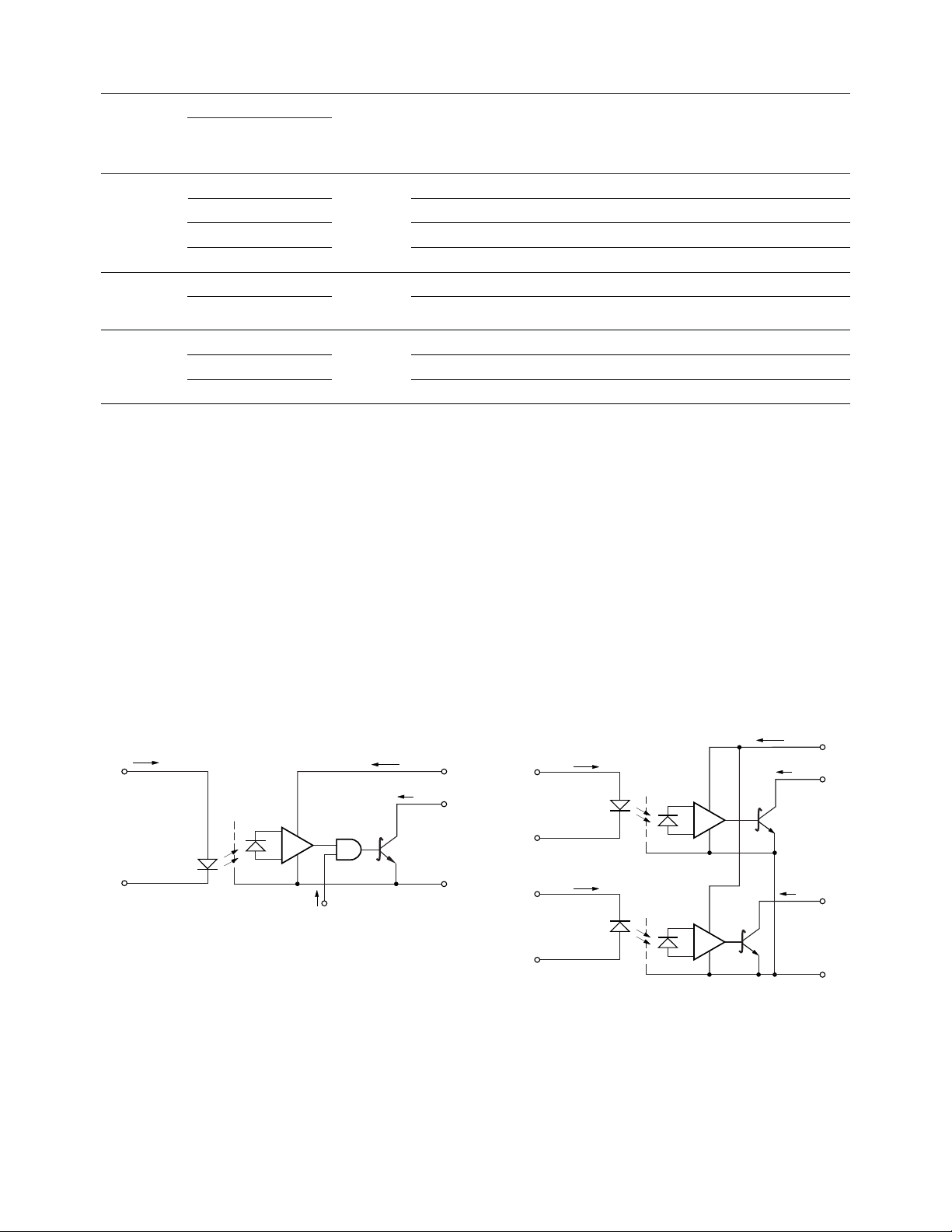
USE OF A 0.1 µF BYPASS CAPACITOR CONNECTED
BETWEEN PINS 5 AND 8 IS RECOMMENDED (SEE NOTE 5).
–
I
F
I
CC
V
CC
V
O
GND
I
O
V
E
I
E
7
6N137, HCPL-2601/2611
HCPL-0600/0601/0611
HCNW137, HCNW2601/2611
SHIELD
8
7
+
2
V
F1
–
I
F1
I
CC
V
CC
V
O1
I
O1
1
SHIELD
6
5
–
4
V
F2
+
I
F2
V
O2
GND
I
O2
3
HCPL-2630/2631/4661
HCPL-0630/0631/0661
Option
UL 5000 Vrms/
Part
Number
HCPL-0600
HCPL-0601
HCPL-0611
HCPL-0630
HCPL-0631
HCPL-0661
HCNW137
HCNW2601
HCNW2611
RoHS
Compliant
Non RoHS
Compliant
Package
-000E No option
-500E #500 X X 1500 per reel
-060E #060 X X 100 per tube
SO-8
-560E #560 X X X 1500 per reel
-000E No option
-500E #500 X X 1500 per reel
SO-8
-000E No option
-300E #300 X X X X 42 per tube
400 mil
DIP-8
-500E #500 X X X X X 750 per reel
Surface
Mount
Gull
Wing
Tape &
Reel
1 Minute
Rating
IEC/EN/DIN
EN 60747-5-2 Quantity
X 100 per tube
X 100 per tube
X X 42 per tube
To order, choose a part number from the part number column and combine with the desired option from the option
column to form an order entry. Combination of Option 020 and Option 060 is not available.
Example 1:
HCPL-2611-560E to order product of 300mil DIP Gull Wing Surface Mount package in Tape and Reel packag
ing with IEC/EN/DIN EN 60747-5-2 Safety Approval in RoHS compliant.
Example 2:
HCPL-2630 to order product of 300mil DIP package in tube packaging and non RoHS compliant.
Option datasheets are available. Contact your Avago sales representative or authorized distributor for information.
Notes:
The notation ‘#XXX’ is used for existing products, while (new) products launched since 15th July 2001 and RoHS compliant option will use ‘-XXXE‘.
Schematic
4
Page 5
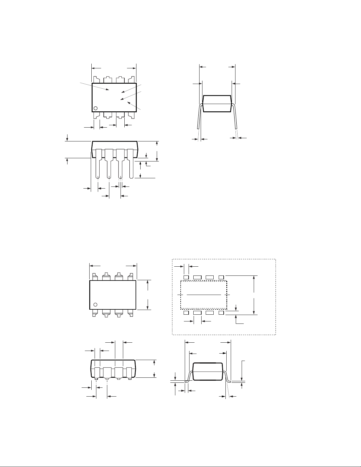
Package Outline Drawings
1.080 ± 0.320
(0.043 ± 0.013)
2.54 ± 0.25
(0.100 ± 0.010)
0.51 (0.020) MIN.
0.65 (0.025) MAX.
4.70 (0.185) MAX.
2.92 (0.115) MIN.
5° TYP.
0.254
+ 0.076
- 0.051
(0.010
+ 0.003)
- 0.002)
7.62 ± 0.25
(0.300 ± 0.010)
6.35 ± 0.25
(0.250 ± 0.010)
9.65 ± 0.25
(0.380 ± 0.010)
1.78 (0.070) MAX.
1.19 (0.047) MAX.
A XXXXZ
YYWW
DATE CODE
DIMENSIONS IN MILLIMETERS AND (INCHES).
5678
4321
OPTION CODE*
UL
RECOGNITION
UR
TYPE NUMBER
*MARKING CODE LETTER FOR OPTION NUMBERS
"L" = OPTION 020
"V" = OPTION 060
OPTION NUMBERS 300 AND 500 NOT MARKED.
NOTE: FLOATING LEAD PROTRUSION IS 0.25 mm (10 mils) MAX.
3.56 ± 0.13
(0.140 ± 0.005)
0.635 ± 0.25
(0.025 ± 0.010)
12° NOM.
9.65 ± 0.25
(0.380 ± 0.010)
0.635 ± 0.130
(0.025 ± 0.005)
7.62 ± 0.25
(0.300 ± 0.010)
5
6
7
8
4
3
2
1
9.65 ± 0.25
(0.380 ± 0.010)
6.350 ± 0.25
(0.250 ± 0.010)
1.016 (0.040)
1.27 (0.050)
10.9 (0.430)
2.0 (0.080)
LAND PATTERN RECOMMENDATION
1.080 ± 0.320
(0.043 ± 0.013)
1.780
(0.070)
MAX.
1.19
(0.047)
MAX.
2.54
(0.100)
BSC
DIMENSIONS IN MILLIMETERS (INCHES).
LEAD COPLANARITY = 0.10 mm (0.004 INCHES).
0.254
+ 0.076
- 0.051
(0.010
+ 0.003)
- 0.002)
NOTE: FLOATING LEAD PROTRUSION IS 0.25 mm (10 mils) MAX.
3.56 ± 0.13
(0.140 ± 0.005)
8-pin DIP Package** (6N137, HCPL-2601/11/30/31, HCPL-4661)
**JEDEC Registered Data (for 6N137 only).
8-pin DIP Package with Gull Wing Surface Mount Option 300
(6N137, HCPL-2601/11/30/31, HCPL-4661)
5
Page 6
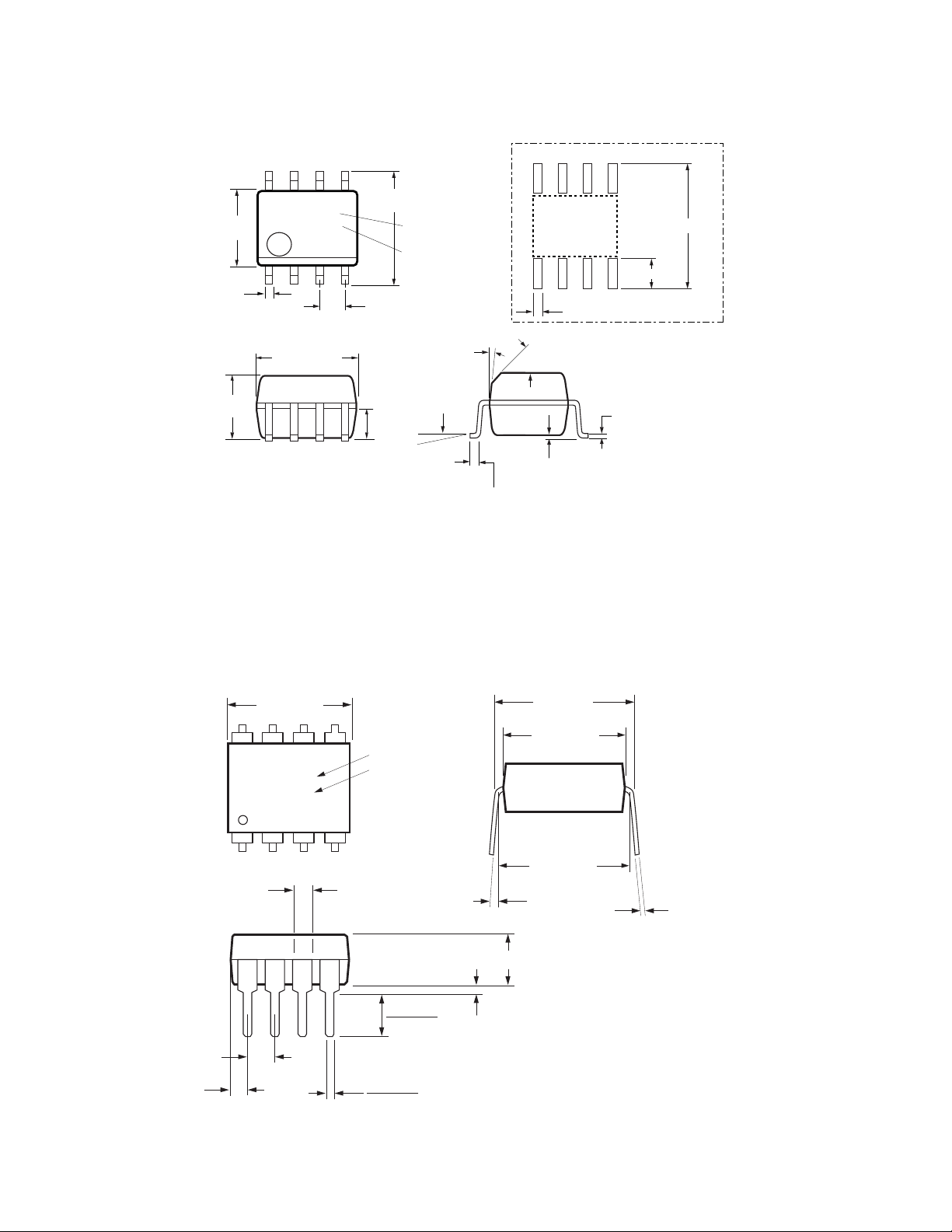
Small-Outline SO-8 Package (HCPL-0600/01/11/30/31/61)
XXX
YWW
8765
4321
5.994 ± 0.203
(0.236 ± 0.008)
3.937 ± 0.127
(0.155 ± 0.005)
0.406 ± 0.076
(0.016 ± 0.003)
1.270
(0.050)
BSC
5.080 ± 0.127
(0.200 ± 0.005)
3.175 ± 0.127
(0.125 ± 0.005)
1.524
(0.060)
45° X
0.432
(0.017)
0.228 ± 0.025
(0.009 ± 0.001)
TYPE NUMBER
(LAST 3 DIGITS)
DATE CODE
0.305
(0.012)
MIN.
TOTAL PACKAGE LENGTH (INCLUSIVE OF MOLD FLASH)
5.207 ± 0.254 (0.205 ± 0.010)
DIMENSIONS IN MILLIMETERS (INCHES).
LEAD COPLANARITY = 0.10 mm (0.004 INCHES) MAX.
NOTE: FLOATING LEAD PROTRUSION IS 0.15 mm (6 mils) MAX.
0.203 ± 0.102
(0.008 ± 0.004)
7°
PIN ONE
0 ~ 7°
*
*
7.49 (0.295)
1.9 (0.075)
0.64 (0.025)
LAND PATTERN RECOMMENDATION
5
6
7
8
4
3
2
1
11.23 ± 0.15
(0.442 ± 0.006)
1.80 ± 0.15
(0.071 ± 0.006)
5.10
(0.201)
MAX.
1.55
(0.061)
MAX.
2.54 (0.100)
TYP.
DIMENSIONS IN MILLIMETERS (INCHES).
NOTE: FLOATING LEAD PROTRUSION IS 0.25 mm (10 mils) MAX.
7° TYP.
0.254
+ 0.076
- 0.0051
(0.010
+ 0.003)
- 0.002)
11.00
(0.433)
9.00 ± 0.15
(0.354 ± 0.006)
MAX.
10.16 (0.400)
TYP.
A
HCNWXXXX
YYWW
DATE CODE
TYPE NUMBER
0.51 (0.021) MIN.
0.40 (0.016)
0.56 (0.022)
3.10 (0.122)
3.90 (0.154)
8-Pin Widebody DIP Package (HCNW137, HCNW2601/11)
6
Page 7
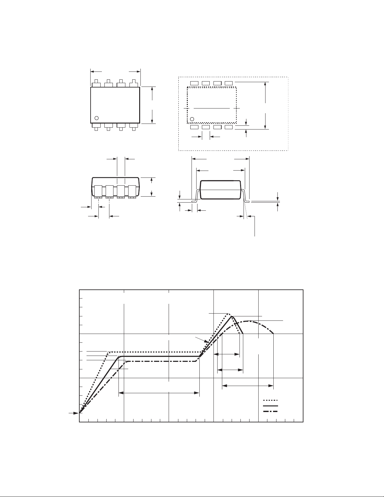
8-Pin Widebody DIP Package with Gull Wing Surface Mount Option 300
(HCNW137, HCNW2601/11)
11.23 ± 0.15
(0.442 ± 0.006)
7
8
6
5
LAND PATTERN RECOMMENDATION
1
2
1.80 ± 0.15
(0.071 ± 0.006)
DIMENSIONS IN MILLIMETERS (INCHES).
LEAD COPLANARITY = 0.10 mm (0.004 INCHES).
NOTE: FLOATING LEAD PROTRUSION IS 0.25 mm (10 mils) MAX.
Solder Re ow Temperature Pro le
3
2.54
(0.100)
BSC
(0.354 ± 0.006)
4
1.55
(0.061)
MAX.
9.00 ± 0.15
4.00
MAX.
(0.158)
(0.030 ± 0.010)
0.75 ± 0.25
1.3
(0.051)
12.30 ± 0.30
(0.484 ± 0.012)
11.00
(0.433)
1.00 ± 0.15
(0.039 ± 0.006)
MAX.
2.29
(0.09)
7° NOM.
13.56
(0.534)
0.254
(0.010
+ 0.076
- 0.0051
+ 0.003)
- 0.002)
ROOM
TEMPERATURE
300
PREHEATING RATE 3 °C + 1 °C/–0.5 °C/SEC.
REFLOW HEATING RATE 2.5 °C ± 0.5 °C/SEC.
200
160 °C
150 °C
140 °C
TEMPERATURE (°C)
100
0
0
NOTE: NON-HALIDE FLUX SHOULD BE USED.
PEAK
TEMP.
245 °C
PEAK
TEMP.
240 °C
PEAK
TEMP.
230 °C
2.5 C ± 0.5 °C/SEC.
30
SEC.
SOLDERING
TIME
200 °C
30
3 °C + 1 °C/–0.5 °C
PREHEATING TIME
150 °C, 90 + 30 SEC.
SEC.
50 SEC.
TIGHT
TYPICAL
LOOSE
50 150100 200 250
TIME (SECONDS)
7
Page 8
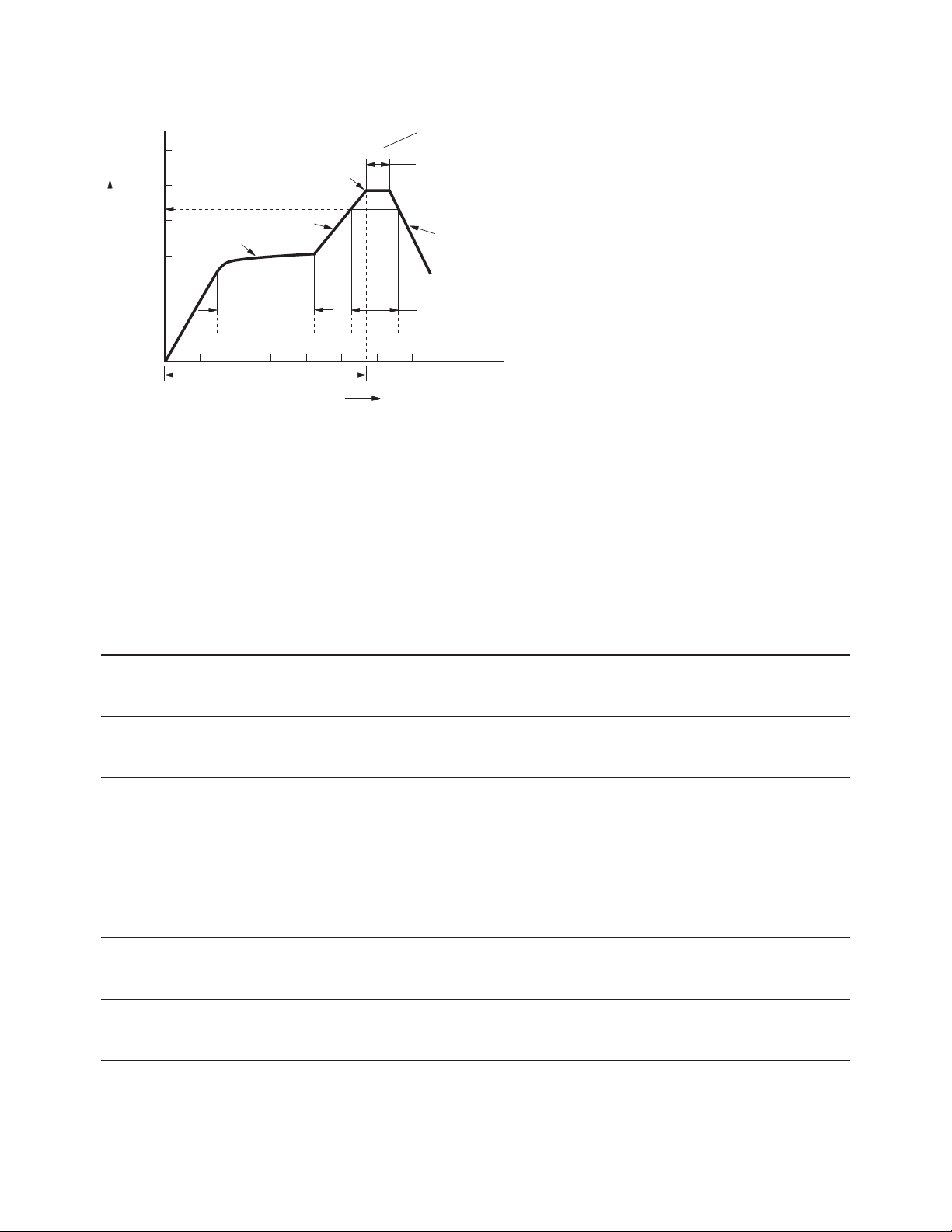
Recommended Pb-free IR Pro le
T
p
217 °C
T
TEMPERATURE
L
smax
smin
150 - 200 °C
T
T
RAMP-UP
3 °C/SEC. MAX.
t
s
PREHEAT
60 to 180 SEC.
* 260 +0/-5 °C
TIME WITHIN 5 °C of ACTUAL
PEAK TEMPERATURE
t
p
15 SEC.
RAMP-DOWN
6 °C/SEC. MAX.
t
L
60 to 150 SEC.
NOTES:
THE TIME FROM 25 °C to PEAK
TEMPERATURE = 8 MINUTES MAX.
= 200 °C, T
T
smax
NOTE: NON-HALIDE FLUX SHOULD BE USED.
* RECOMMENDED PEAK TEMPERATURE FOR
WIDEBODY 400mils PACKAGE IS 245 °C
smin
= 150 °C
25
t 25 °C to PEAK
TIME
Regulatory Information
The 6N137, HCPL-26XX/06XX/46XX, and HCNW137/26XX have been approved by the following organizations:
UL
Recognized under UL 1577, Component Recognition
Program, File E55361.
CSA
Approved under CSA Component Acceptance Notice
#5, File CA 88324.
Insulation and Safety Related Speci cations
8-pin DIP Widebody
(300 Mil) SO-8 (400 Mil)
Parameter Symbol Value Value Value Units Conditions
Minimum External L(101) 7.1 4.9 9.6 mm Measured from input terminals
Air Gap (External to output terminals, shortest
Clearance) distance through air.
Minimum External L(102) 7.4 4.8 10.0 mm Measured from input terminals
Tracking (External to output terminals, shortest
Creepage) distance path along body.
Minimum Internal 0.08 0.08 1.0 mm Through insulation distance,
Plastic Gap conductor to conductor, usually
(Internal Clearance) the direct distance between the
photoemitter and photodetector
inside the optocoupler cavity.
Minimum Internal NA NA 4.0 mm Measured from input terminals
Tracking (Internal to output terminals, along
Creepage) internal cavity.
Tracking Resistance CTI 200 200 200 Volts DIN IEC 112/VDE 0303 Part 1
(Comparative
Tracking Index)
Isolation Group IIIa IIIa IIIa Material Group
(DIN VDE 0110, 1/89, Table 1)
IEC/EN/DIN EN 60747-5-2
Approved under
IEC 60747-5-2:1997 + A1:2002
EN 60747-5-2:2001 + A1:2002
DIN EN 60747-5-2 (VDE 0884 Teil 2):2003-01
(Option 060 and HCNW only)
Option 300 - surface mount classi cation is Class A in accordance with CECC 00802.
8
Page 9

IEC/EN/DIN EN 60747-5-2 Insulation Related Characteristics
(HCPL-06xx Option 060 Only)
Description Symbol Characteristic Units
Installation classi cation per DIN VDE 0110/1.89, Table 1
for rated mains voltage ≤ 150 V rms I-IV
for rated mains voltage ≤ 300 V rms I-III
for rated mains voltage ≤ 600 V rms I-III
Climatic Classi cation 55/85/21
Pollution Degree (DIN VDE 0110/1.89) 2
Maximum Working Insulation Voltage V
Input to Output Test Voltage, Method b*
V
x 1.875 = VPR, 100% Production Test with tm = 1 sec, VPR 1063 V
IORM
Partial Discharge < 5 pC
Input to Output Test Voltage, Method a*
V
x 1.5 = VPR, Type and Sample Test, VPR 851 V
IORM
tm = 60 sec, Partial Discharge < 5 pC
Highest Allowable Overvoltage
(Transient Overvoltage, t
= 10 sec) V
ini
Safety Limiting Values
(Maximum values allowed in the event of a failure)
Case Temperature T
Input Current** I
Output Power** P
Insulation Resistance at T
, VIO = 500 V RS ≥109
S
567 V
IORM
6000 V
IOTM
150 °C
S
150 mA
S,INPUT
600 mW
S,OUTPUT
peak
peak
peak
peak
*Refer to the front of the optocoupler section of the current catalog, under Product Safety Regulations section, IEC/EN/DIN EN 60747-5-2, for a
detailed description.
Note: Isolation characteristics are guaranteed only within the safety maximum ratings which must be ensured by protective circuits in application.
9
Page 10

IEC/EN/DIN EN 60747-5-2 Insulation Related Characteristics
(HCPL-26xx; 46xx; 6N13x Option 060 Only)
Description Symbol Characteristic Units
Installation classi cation per DIN VDE 0110/1.89, Table 1
for rated mains voltage ≤ 300 V rms I-IV
for rated mains voltage ≤ 450 V rms I-III
Climatic Classi cation 55/85/21
Pollution Degree (DIN VDE 0110/1.89) 2
Maximum Working Insulation Voltage V
Input to Output Test Voltage, Method b*
V
x 1.875 = VPR, 100% Production Test with tm = 1 sec, VPR 1181 V
IORM
Partial Discharge < 5 pC
Input to Output Test Voltage, Method a*
V
x 1.5 = VPR, Type and sample test, VPR 945 V
IORM
tm = 60 sec, Partial Discharge < 5 pC
Highest Allowable Overvoltage*
(Transient Overvoltage, t
= 10 sec) V
ini
Safety Limiting Values
(Maximum values allowed in the event of a failure,
also see Figure 16, Thermal Derating curve.)
Case Temperature T
Input Current I
Output Power P
Insulation Resistance at T
*Refer to the front of the optocoupler section of the current catalog, under Product Safety Regulations section, IEC/EN/DIN EN 60747-5-2, for a
detailed description.
Note: Isolation characteristics are guaranteed only within the safety maximum ratings which must be ensured by protective circuits in application.
, VIO = 500 V RS ≥109
S
630 V
IORM
6000 V
IOTM
175 °C
S
230 mA
S,INPUT
600 mW
S,OUTPUT
peak
peak
peak
peak
IEC/EN/DIN EN 60747-5-2 Insulation Related Characteristics (HCNW137/2601/2611 Only)
Description Symbol Characteristic Units
Installation classi cation per DIN VDE 0110/1.89, Table 1
for rated mains voltage ≤600 V rms I-IV
for rated mains voltage ≤1000 V rms I-III
Climatic Classi cation (DIN IEC 68 part 1) 55/100/21
Pollution Degree (DIN VDE 0110/1.89) 2
Maximum Working Insulation Voltage V
Input to Output Test Voltage, Method b*
V
x 1.875 = VPR, 100% Production Test with tm = 1 sec, VPR 2651 V
IORM
Partial Discharge < 5 pC
Input to Output Test Voltage, Method a*
V
x 1.5 = VPR, Type and sample test, VPR 2121 V
IORM
tm = 60 sec, Partial Discharge < 5 pC
Highest Allowable Overvoltage*
(Transient Overvoltage, t
= 10 sec) V
ini
Safety Limiting Values
(Maximum values allowed in the event of a failure,
also see Figure 16, Thermal Derating curve.)
Case Temperature T
Input Current I
Output Power P
Insulation Resistance at T
*Refer to the front of the optocoupler section of the current catalog, under Product Safety Regulations section, IEC/EN/DIN EN 60747-5-2, for a
detailed description.
Note: Isolation characteristics are guaranteed only within the safety maximum ratings which must be ensured by protective circuits in application.
, VIO = 500 V RS ≥109
S
1414 V
IORM
8000 V
IOTM
150 °C
S
400 mA
S,INPUT
700 mW
S,OUTPUT
peak
peak
peak
peak
10
Page 11

Absolute Maximum Ratings* (No Derating Required up to 85°C)
Parameter Symbol Package** Min. Max. Units Note
Storage Temperature TS -55 125 °C
Operating Temperature† T
Average Forward Input Current I
Single SO-8
Widebody
Dual 8-Pin DIP 15 1, 3
Dual SO-8
Reverse Input Voltage V
Widebody 3
Input Power Dissipation P
Supply Voltage V
(1 Minute Maximum)
Enable Input Voltage (Not to VE Single 8-Pin DIP VCC + 0.5 V
Exceed V
by more than Single SO-8
CC
500 mV) Widebody
Enable Input Current IE 5 mA
Output Collector Current I
Output Collector Voltage V
Output Collector Power P
Dissipation Single SO-8
Widebody
Dual 8-Pin DIP 60 1, 4
Dual SO-8
Lead Solder Temperature T
(Through Hole Parts Only) 1.6 mm below seating plane
Widebody 260°C for 10 sec.,
up to seating plane
Solder Re ow Temperature SO-8 and See Package Outline
Pro le (Surface Mount Parts Only) Option 300 Drawings section
-40 85 °C
A
Single 8-Pin DIP 20 mA 2
F
8-Pin DIP, SO-8 5 V 1
R
Widebody 40 mW
I
7 V
CC
50 mA 1
O
7 V 1
O
Single 8-Pin DIP 85 mW
O
8-Pin DIP 260°C for 10 sec.,
LS
*JEDEC Registered Data (for 6N137 only).
**Ratings apply to all devices except otherwise noted in the Package column.
†0°C to 70°C on JEDEC Registration.
Recommended Operating Conditions
Parameter Symbol Min. Max. Units
Input Current, Low Level IFL* 0 250 µA
[1]
Input Current, High Level
I
Power Supply Voltage V
Low Level Enable Voltage† V
High Level Enable Voltage† V
Operating Temperature T
Fan Out (at R
= 1 k)
L
N 5 TTL Loads
[1]
Output Pull-up Resistor R
*The o condition can also be guaranteed by ensuring that VFL ≤0.8 volts.
**The initial switching threshold is 5 mA or less. It is recommended that 6.3 mA to 10 mA be used for best performance and to permit at least a 20%
LED degradation guardband.
†For single channel products only.
11
** 5 15 mA
FH
4.5 5.5 V
CC
0 0.8 V
EL
2.0 VCC V
EH
-40 85 °C
A
330 4 k
L
Page 12

Electrical Speci cations
Over recommended temperature (TA = -40°C to +85°C) unless otherwise speci ed. All Typicals at VCC = 5 V, TA = 25°C.
All enable test conditions apply to single channel products only. See note 5.
Parameter Sym. Package Min. Typ. Max. Units Test Conditions Fig. Note
High Level Output IOH* All 5.5 100 µA VCC = 5.5 V, VE = 2.0 V, 1 1, 6,
Current V
Input Threshold I
Single Channel 2.0 5.0 mA VCC = 5.5 V, VE = 2.0 V, 2, 3 19
TH
Current Widebody V
Low Level Output V
Dual Channel 2.5
* 8-Pin DIP 0.35 0.6 V VCC = 5.5 V, VE = 2.0 V, 2, 3, 1, 19
OL
Voltage SO-8 I
Widebody 0.4 I
High Level Supply I
Single Channel 7.0 10.0* mA VE = 0.5 V VCC = 5.5 V 7
CCH
Current 6.5 V
Dual Channel 10 15 Both
Channels
= 5.5 V, IF = 250 A 19
O
= 0.6 V,
O
IOL (Sinking) = 13 mA
= 5 mA, 4, 5
F
(Sinking) = 13 mA
OL
= VCC IF = 0 mA
E
Low Level Supply I
Current 8.5 V
Single Channel 9.0 13.0* mA VE = 0.5 V VCC = 5.5 V 8
CCL
= VCC IF = 10 mA
E
Dual Channel 13 21 Both
Channels
High Level Enable I
Single Channel -0.7 -1.6 mA VCC = 5.5 V, VE = 2.0 V
EH
Current
Low Level Enable I
* -0.9 -1.6 mA VCC = 5.5 V, VE = 0.5 V 9
EL
Current
High Level Enable V
2.0 V 19
EH
Voltage
Low Level Enable V
0.8 V
EL
Voltage
Input Forward V
8-Pin DIP 1.4 1.5 1.75* V TA = 25°C IF = 10 mA 6, 7 1
F
Voltage SO-8 1.3 1.80
Widebody 1.25 1.64 1.85 T
= 25°C
A
1.2 2.05
Input Reverse BV
* 8-Pin DIP 5 V IR = 10 A 1
R
Breakdown SO-8
Voltage Widebody 3 I
Input Diode DV
Temperature ∆T
8-Pin DIP -1.6 mV/°C IF = 10 mA 7 1
F/
SO-8
A
= 100 µA, TA = 25°C
R
Coe cient Widebody -1.9
Input Capacitance C
8-Pin DIP 60 pF f = 1 MHz, VF = 0 V 1
IN
SO-8
Widebody 70
*JEDEC registered data for the 6N137. The JEDEC Registration speci es 0°C to +70°C. HP speci es -40°C to +85°C.
12
Page 13

Switching Speci cations (AC)
Over Recommended Temperature (T
= -40°C to +85°C), VCC = 5 V, I
A
= 7.5 mA unless otherwise speci ed.
F
All Typicals at TA = 25°C, VCC = 5 V.
Parameter Sym. Package** Min. Typ. Max. Units Test Conditions Fig. Note
Propagation Delay t
Time to High 100 C
Output Level
Propagation Delay t
Time to Low 100 19
Output Level
Pulse Width |t
Distortion SO-8 10,
Widebody 40 11
Propagation Delay t
Skew 19
Output Rise t
Time (10-90%)
Output Fall t
Time (90-10%)
Propagation Delay t
Time of Enable C
from V
to V
EH
EL
Propagation Delay t
Time of Enable
from V
EL
to V
EH
20 48 75* ns TA = 25°C RL = 350 8, 9, 1, 10,
PLH
25 50 75* ns TA = 25°C 1, 11,
PHL
- t
| 8-Pin DIP 3.5 35 ns 8, 9, 13, 19
PHL
PLH
40 ns 12, 13,
PSK
24 ns 12 1, 19
r
10 ns 12 1, 19
f
Single Channel 30 ns RL = 350 , 13, 14
ELH
= 15 pF, 14
L
= 15 pF 10 19
L
VEL = 0 V, VEH = 3 V
Single Channel 20 ns 15
EHL
*JEDEC registered data for the 6N137.
**Ratings apply to all devices except otherwise noted in the Package column.
Parameter Sym. Device Min. Typ. Units Test Conditions Fig. Note
Logic High |CMH| 6N137 1,000 10,000 V/µs |VCM| = 10 V VCC = 5 V, IF = 0 mA, 15 1, 16,
Common HCPL-2630 5,000 10,000 |V
Mode HCPL-0600/0630 R
Transient HCNW137
Immunity HCPL-2601/2631 10,000 15,000 |V
HCPL-0601/0631
HCNW2601
HCPL-2611/4661 15,000 25,000 |V
HCPL-0611/0661
HCNW2611
Logic Low |CM
| 6N137 1,000 10,000 V/µs |VCM| = 10 V VCC = 5 V, IF = 7.5 mA, 15 1, 17,
L
Common HCPL-2630 5,000 10,000 |V
Mode HCPL-0600/0630 R
Transient HCNW137
Immunity HCPL-2601/2631 10,000 15,000 |V
HCPL-0601/0631
HCNW2601
HCPL-2611/4661 15,000 25,000 |V
HCPL-0611/0661
HCNW2611
| = 1 kV V
CM
| = 1 kV
CM
| = 1 kV
CM
| = 1 kV V
CM
| = 1 kV
CM
| = 1 kV
CM
= 2 V, 18, 19
O(MIN)
= 350 , TA = 25°C
L
= 0.8 V, 18, 19
O(MAX)
= 350 , TA = 25°C
L
13
Page 14

Package Characteristics
All Typicals at TA = 25°C.
Parameter Sym. Package Min. Typ. Max. Units Test Conditions Fig. Note
Input-Output I
Insulation Single SO-8 V
Input-Output V
Momentary With- Widebody 5000 T
stand Voltage** OPT 020† 5000
Input-Output R
Resistance Widebody 10
10
Input-Output C
Capacitance Widebody 0.5 0.6 23
Input-Input I
Insulation V
Leakage Current
Resistance R
(Input-Input)
Capacitance C
(Input-Input) Dual SO-8 0.25
*JEDEC registered data for the 6N137. The JEDEC Registration speci es 0°C to 70°C. Avago speci es -40°C to 85°C.
**The Input-Output Momentary Withstand Voltage is a dielectric voltage rating that should not be interpreted as an input-output continuous voltage rating. For the continuous voltage rating refer to the IEC/EN/DIN EN 60747-5-2 Insulation Characteristics Table (if applicable), your equipment
level safety speci cation or Avago Application Note 1074 entitled “Optocoupler Input-Output Endurance Voltage.”
†For 6N137, HCPL-2601/2611/2630/2631/4661 only.
* Single 8-Pin DIP 1 A 45% RH, t = 5 s, 20, 21
I-O
8-Pin DIP, SO-8 3750 V rms RH ≤ 50%, t = 1 min, 20, 21
ISO
8-Pin DIP, SO-8 1012 V
I-O
8-Pin DIP, SO-8 0.6 pF f = 1 MHz, TA = 25°C 1, 20,
I-O
Dual Channel 0.005 A RH ≤ 45%, t = 5 s, 24
I-I
Dual Channel 1011 24
I-I
Dual 8-Pin DIP 0.03 pF f = 1 MHz 24
I-I
12
1013 TA = 25°C 23
11
TA = 100°C
= 3 kV dc, TA = 25°C
I-O
= 25°C 20, 22
A
= 500 V dc 1, 20,
I-O
= 500 V
I-I
Notes:
1. Each channel.
2. Peaking circuits may produce transient input currents up to 50 mA, 50 ns maximum pulse width, provided average current does not exceed 20 mA.
3. Peaking circuits may produce transient input currents up to 50 mA, 50 ns maximum pulse width, provided average current does not exceed 15 mA.
4. Derate linearly above 80°C free-air temperature at a rate of 2.7 mW/°C for the SOIC-8 package.
5. Bypassing of the power supply line is required, with a 0.1 µF ceramic disc capacitor adjacent to each optocoupler as illustrated in Figure 17. Total
lead length between both ends of the capacitor and the isolator pins should not exceed 20 mm.
6. The JEDEC registration for the 6N137 speci es a maximum IOH of 250 µA. Avago guarantees a maximum IOH of 100 A.
7. The JEDEC registration for the 6N137 speci es a maximum I
8. The JEDEC registration for the 6N137 speci es a maximum I
9. The JEDEC registration for the 6N137 speci es a maximum IEL of –2.0 mA. Avago guarantees a maximum IEL of -1.6 mA.
10. The t
11. The t
12. t
13. See application section titled “Propagation Delay, Pulse-Width Distortion and Propagation Delay Skew” for more information.
14. The t
15. The t
16. CM
17. CM
18. For sinusoidal voltages, (|dV
19. No external pull up is required for a high logic state on the enable input. If the V
propagation delay is measured from the 3.75 mA point on the falling edge of the input pulse to the 1.5 V point on the rising edge of the
PLH
output pulse.
propagation delay is measured from the 3.75 mA point on the rising edge of the input pulse to the 1.5 V point on the falling edge of the
PHL
output pulse.
is equal to the worst case di erence in t
PSK
enable propagation delay is measured from the 1.5 V point on the falling edge of the enable input pulse to the 1.5 V point on the rising edge
ELH
of the output pulse.
enable propagation delay is measured from the 1.5 V point on the rising edge of the enable input pulse to the 1.5 V point on the falling edge
EHL
of the output pulse.
is the maximum tolerable rate of rise of the common mode voltage to assure that the output will remain in a high logic state (i.e., VO > 2.0 V).
H
is the maximum tolerable rate of fall of the common mode voltage to assure that the output will remain in a low logic state (i.e., VO < 0.8 V).
L
CM
| / dt)
max
and/or t
PHL
= fCMVCM(p-p).
performance. For single channel products only.
of 15 mA. Avago guarantees a maximum I
CCH
of 18 mA. Avago guarantees a maximum I
CCL
that will be seen between units at any given temperature and speci ed test conditions.
PLH
pin is not used, tying VE to VCC will result in improved CMR
E
of 10 mA.
CCH
of 13 mA.
CCL
20. Device considered a two-terminal device: pins 1, 2, 3, and 4 shorted together, and pins 5, 6, 7, and 8 shorted together.
21. In accordance with UL1577, each optocoupler is proof tested by applying an insulation test voltage ≥ 4500 V rms for one second (leakage detection
current limit, I
5-2 Insulation Characteristics Table, if applicable.
≤ 5 A). This test is performed before the 100% production test for partial discharge (Method b) shown in the IEC/EN/DIN EN 60747-
I-O
22. In accordance with UL 1577, each optocoupler is proof tested by applying an insulation test voltage ≥ 6000 V rms for one second (leakage detection
current limit, I
5-2 Insulation Characteristics Table, if applicable.
≤ 5 A). This test is performed before the 100% production test for partial discharge (Method b) shown in the IEC/EN/DIN EN 60747-
I-O
23. Measured between the LED anode and cathode shorted together and pins 5 through 8 shorted together. For dual channel products only.
24. Measured between pins 1 and 2 shorted together, and pins 3 and 4 shorted together. For dual channel products only
14
Page 15
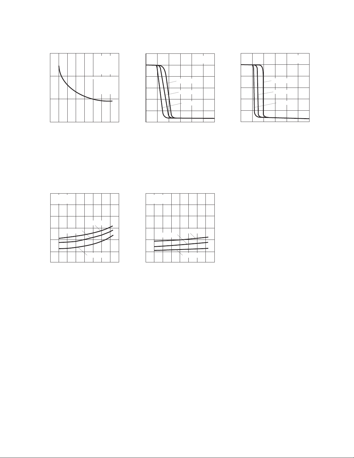
15
10
5
– HIGH LEVEL OUTPUT CURRENT – µA
0
-60
-40 0 40 80
OH
I
-20
TA – TEMPERATURE – °C
* FOR SINGLE
CHANNEL
PRODUCTS
ONLY
20
V
= 5.5 V
CC
= 5.5 V
V
O
= 2.0 V*
V
E
= 250 µA
I
F
60
Figure 1. Typical high level output current vs.
temperature.
100
6
5
4
3
2
– OUTPUT VOLTAGE – V
1
O
V
0
0
– FORWARD INPUT CURRENT – mA
I
F
8-PIN DIP, SO-8
VCC = 5 V
T
= 25 °C
A
RL = 350 Ω
RL = 1 KΩ
RL = 4 KΩ
123456
– OUTPUT VOLTAGE – V
O
V
Figure 2. Typical output voltage vs. forward input current.
6
5
4
3
2
1
0
0
– FORWARD INPUT CURRENT – mA
I
F
WIDEBODY
VCC = 5 V
T
= 25 °C
A
RL = 350 Ω
RL = 1 KΩ
RL = 4 KΩ
123456
6
VCC = 5.0 V
V
5
4
3
2
1
– INPUT THRESHOLD CURRENT – mA
0
TH
I
-60 -20 20
8-PIN DIP, SO-8
= 0.6 V
O
RL = 1 KΩ
– TEMPERATURE – °C
T
A
RL = 350 Ω
RL = 4 KΩ
60
– INPUT THRESHOLD CURRENT – mA
100
80400-40
I
Figure 3. Typical input threshold current vs. temperature.
6
VCC = 5.0 V
V
= 0.6 V
O
5
4
3
RL = 1 KΩ
2
1
0
TH
-60 -20 20
– TEMPERATURE – °C
T
A
WIDEBODY
RL = 350 Ω
RL = 4 KΩ
100
80400-40
60
15
Page 16
= 2.0 V*
E
= 5.0 mA
F
8-PIN DIP, SO-8
* FOR SINGLE
CHANNEL
PRODUCTS ONLY
0.8
0.7
VCC = 5.5 V
V
I
0.6
0.5
0.4
IO = 16 mA
IO = 12.8 mA
0.3
0.2
0.1
– LOW LEVEL OUTPUT VOLTAGE – V
OL
V
IO = 9.6 mA
0
-60 -20 20
– TEMPERATURE – °C
T
A
IO = 6.4 mA
60
0.8
0.7
0.6
0.5
0.4
0.3
0.2
0.1
– LOW LEVEL OUTPUT VOLTAGE – V
0
80400-40
100
OL
-60 -20 20
V
WIDEBODY
IO = 16 mA
IO = 9.6 mA
– TEMPERATURE – °C
T
A
VCC = 5.5 V
V
= 2.0 V
E
I
= 5.0 mA
F
IO = 12.8 mA
IO = 6.4 mA
80400-40
60
100
70
VCC = 5.0 V
V
= 2.0 V*
E
V
= 0.6 V
OL
* FOR SINGLE
CHANNEL
PRODUCTS ONLY
60
IF = 10-15 mA
50
40
20
– LOW LEVEL OUTPUT CURRENT – mA
-60 -20 20
OL
I
– TEMPERATURE – °C
T
A
IF = 5.0 mA
80400-40
60
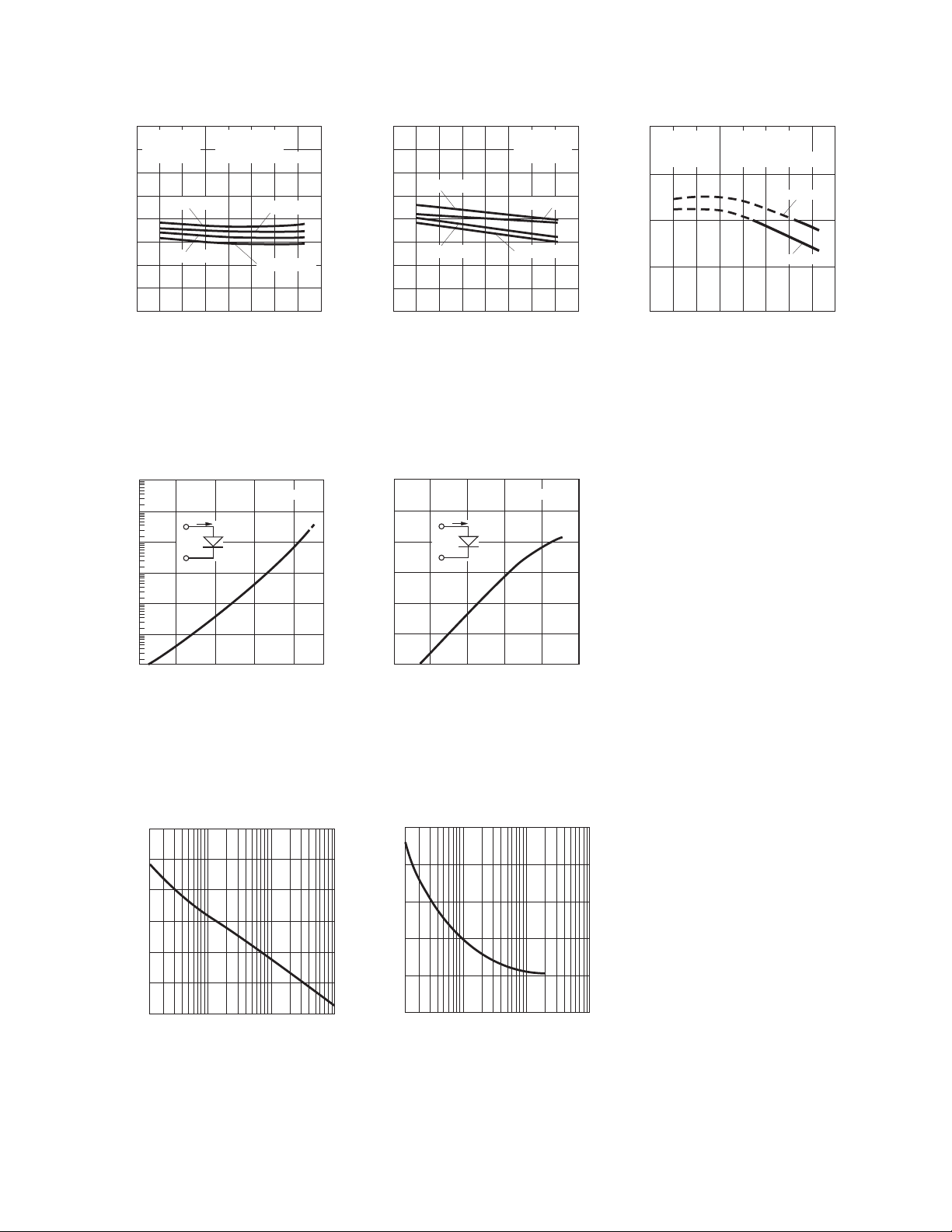
Figure 4. Typical low level output voltage vs. temperature. Figure 5. Typical low level output current vs.
temperature.
100
1000
100
10
8-PIN DIP, SO-8
I
F
+
V
F
–
1.0
0.1
0.01
– FORWARD CURRENT – mA
F
I
0.001
1.1
1.3
VF – FORWARD VOLTAGE – V
T
A
= 25 °C
1.51.2 1.4
1.6
1000
100
0.01
- FORWARD CURRENT - mA
F
I
0.001
10
1.0
0.1
1.2
WIDEBODY
I
F
+
V
F
-
1.4
VF - FORWARD VOLTAGE - V
Figure 6. Typical input diode forward characteristic.
-2.4
8-PIN DIP, SO-8
-2.2
-2.0
-1.8
-1.6
/dT – FORWARD VOLTAGE
F
-1.4
dV
-1.2
TEMPERATURE COEFFICIENT – mV/°C
0.1 1 10 100
I
– PULSE INPUT CURRENT – mA
F
-2.3
-2.2
-2.1
-2.0
/dT – FORWARD VOLTAGE
-1.9
F
dV
-1.8
TEMPERATURE COEFFICIENT – mV/°C
0.1 1 10 100
I
– PULSE INPUT CURRENT – mA
F
Figure 7. Typical temperature coe cient of forward voltage vs. input current.
WIDEBODY
T
A
= 25 oC
1.61.3 1.5
1.7
16
Page 17
I
INPUT
NODE
F
R
M
PULSE GEN.
Z = 50 Ω
O
t = t = 5 ns
r
f
MONITORING
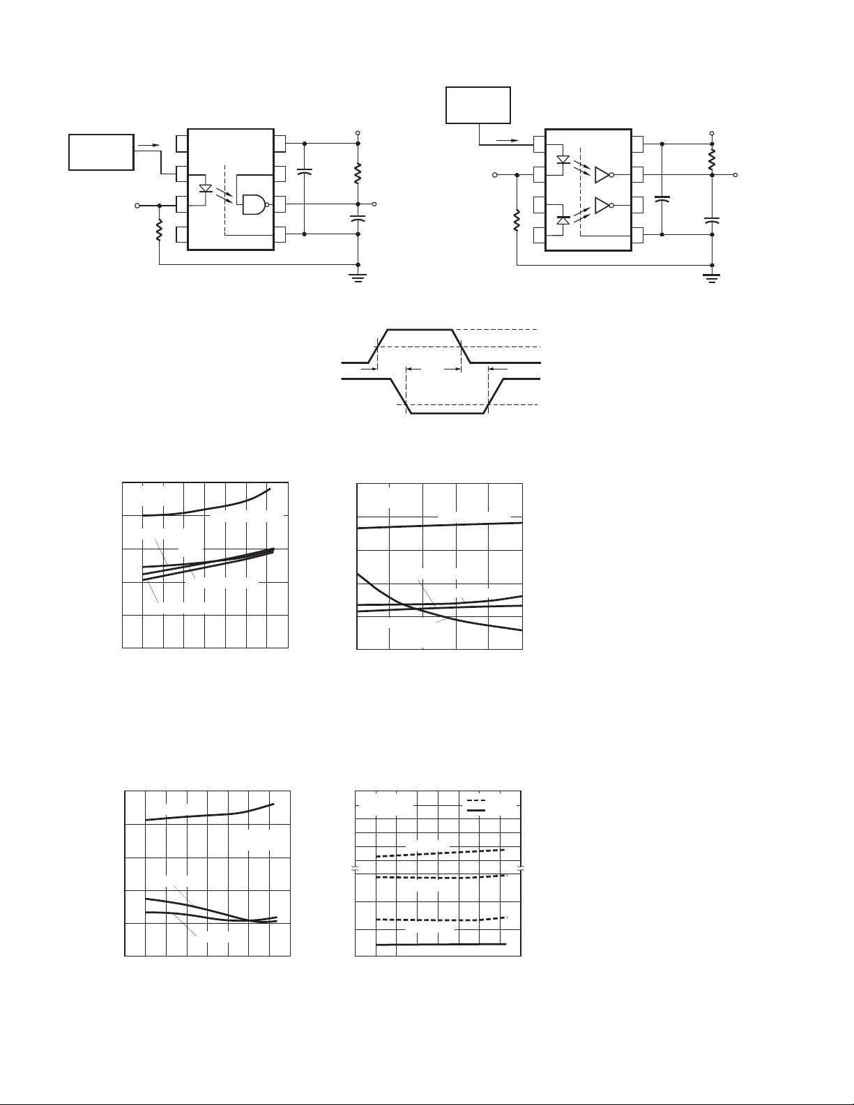
Figure 8. Test circuit for t
SINGLE CHANNEL
1
2
3
4
and t
PHL
PLH
.
V
CC
GND
PULSE GEN.
Z = 50 Ω
O
t = t = 5 ns
r
+5 V
8
0.1µF
7
BYPASS
6
R
L
OUTPUT V
MONITORING
*C
NODE
L
f
MONITORING
O
INPUT
NODE
I
F
R
M
5
*CL IS APPROXIMATELY 15 pF WHICH INCLUDES
PROBE AND STRAY WIRING CAPACITANCE.
INPUT
I
F
OUTPUT
V
t
PHL
O
t
PLH
DUAL CHANNEL
1
2
3
4
I = 7.50 mA
F
I = 3.75 mA
F
1.5 V
V
GND
+5 V
8
CC
7
0.1µF
BYPASS
6
5
R
L
*
C
L
OUTPUT V
MONITORING
NODE
O
100
VCC = 5.0 V
I
= 7.5 mA
F
80
t
, RL = 350 Ω
PHL
60
40
t
, RL = 350 Ω
PLH
20
– PROPAGATION DELAY – ns
P
t
0
-60 -20 20
T
– TEMPERATURE – °C
A
1 KΩ
4 KΩ
t
PLH
t
, RL = 4 KΩ
PLH
, RL = 1 KΩ
60
80400-40
Figure 9. Typical propagation delay vs. temperature.
40
RL = 4 kΩ
30
20
10
RL = 350Ω
VCC = 5.0 V
I
= 7.5 mA
F
0
RL = 1 kΩ
-10
PWD - PULSE WIDTH DISTORTION - ns
-60
-20 20
T
- TEMPERATURE -oC
A
80400-40
60
Figure 11. Typical pulse width distortion vs.
temperature.
100
100
105
VCC = 5.0 V
T
= 25°C
A
90
t
PLH
, RL = 4 KΩ
75
t
, RL = 350 Ω
60
45
– PROPAGATION DELAY – ns
P
t
30
5913
PLH
t
, RL = 1 KΩ
PLH
t
, RL = 350 Ω
PHL
– PULSE INPUT CURRENT – mA
I
F
1 KΩ
4 KΩ
15117
Figure 10. Typical propagation delay vs. pulse
input current.
VCC = 5.0 V
= 7.5 mA
I
F
R
300
= 4 kΩ
L
290
60
RL = 1 kΩ
40
– RISE, FALL TIME – ns
f
, t
20
r
t
0
-60
RL = 350 Ω
RL = 350 Ω, 1 kΩ, 4 kΩ
-20
– TEMPERATURE – °C
T
A
20 60-40 0 40 80
t
RISE
t
FALL
100
Figure 12. Typical rise and fall time vs. temperature.
17
Page 18
PULSE GEN.
Z = 50 Ω
O
t = t = 5 ns
f
r
7.5 mA
I
F
INPUT V
E
MONITORING NODE
1
2
3
4
V
GND
+5 V
8
CC
0.1 µF
7
BYPASS
6
5
R
L
OUTPUT V
MONITORING
*C
NODE
L
O
INPUT
V
E
t
EHL
OUTPUT
V
O
*C IS APPROXIMATELY 15 pF WHICH INCLUDES
L
PROBE AND STRAY WIRING CAPACITANCE.
t
ELH
3.0 V
1.5 V
1.5 V
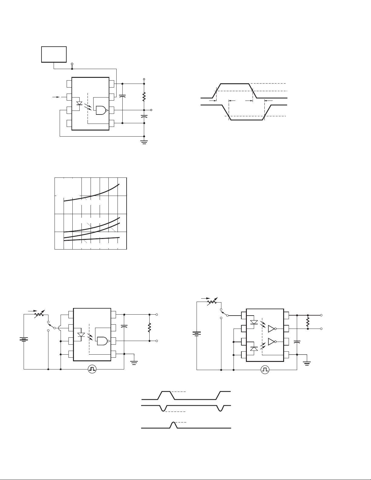
Figure 13. Test circuit for t
120
VCC = 5.0 V
= 3.0 V
V
EH
= 0 V
V
EL
= 7.5 mA
I
F
90
t
ELH
EHL
, RL = 4 kΩ
60
t
, RL = 1 kΩ
ELH
30
t
, RL = 350 Ω, 1 kΩ, 4 kΩ
– ENABLE PROPAGATION DELAY – ns
0
E
-60
t
-20
EHL
20 60-40 0 40 80
TA – TEMPERATURE – °C
Figure 14. Typical enable propagation delay vs.
temperature.
I
F
B
A
V
FF
SINGLE CHANNEL
1
2
3
4
and t
t
ELH
.
ELH
, RL = 350 Ω
V
8
CC
7
6
GND
5
100
0.1 µF
BYPASS
+5 V
R
L
OUTPUT V
MONITORING
NODE
I
F
B
A
V
O
FF
DUAL CHANNEL
1
2
3
4
V
CC
GND
R
L
+5 V
OUTPUT V
MONITORING
NODE
O
8
7
0.1 µF
6
BYPASS
5
V
CM
+
–
PULSE
GENERATOR
Z = 50 Ω
O
V
CM
0 V
SWITCH AT A: I = 0 mA
5 V
V
O
SWITCH AT B: I = 7.5 mA
V
O
0.5 V
F
F
V (PEAK)
CM
V (MIN.)
O
V (MAX.)
O
Figure 15. Test circuit for common mode transient immunity and typical waveforms.
18
CM
CM
H
L
V
CM
+
–
PULSE
GENERATOR
Z = 50 Ω
O
Page 19
S
800
700
600
500
, INPUT CURRENT – I
400
S
300
200
100
OUTPUT POWER – P
HCPL-2611 OPTION 060
0
0
TS – CASE TEMPERATURE – °C
PS (mW)
I
(mA)
S
12525 75 100 150
175
20050
S
800
700
600
, INPUT CURRENT – I
500
S
400
300
200
100
0
0
OUTPUT POWER – P
TS – CASE TEMPERATURE – °C
HCNWXXXX
PS (mW)
I
S
(mA)
12525 75 100 150
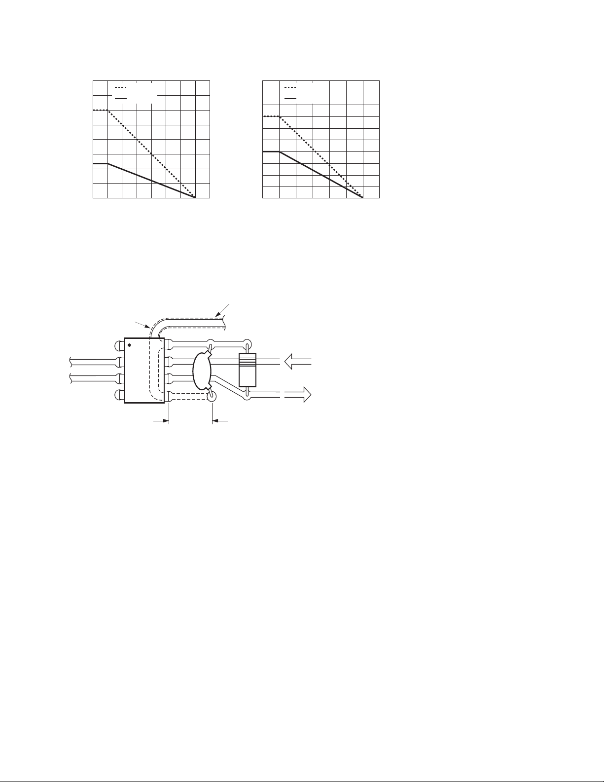
Figure 16. Thermal derating curve, dependence of safety limiting value with case temperature
per IEC/EN/DIN EN 60747-5-2.
GND BUS (BACK)
VCC BUS (FRONT)
NC
ENABLE
0.1µF
17550
NC
10 mm MAX.
(SEE NOTE 5)
Figure 17. Recommended printed circuit board layout.
OUTPUT
SINGLE CHANNEL
DEVICE ILLUSTRATED.
19
Page 20
SINGLE CHANNEL DEVICE
5 V
V
CC1
470 Ω
GND 1
1
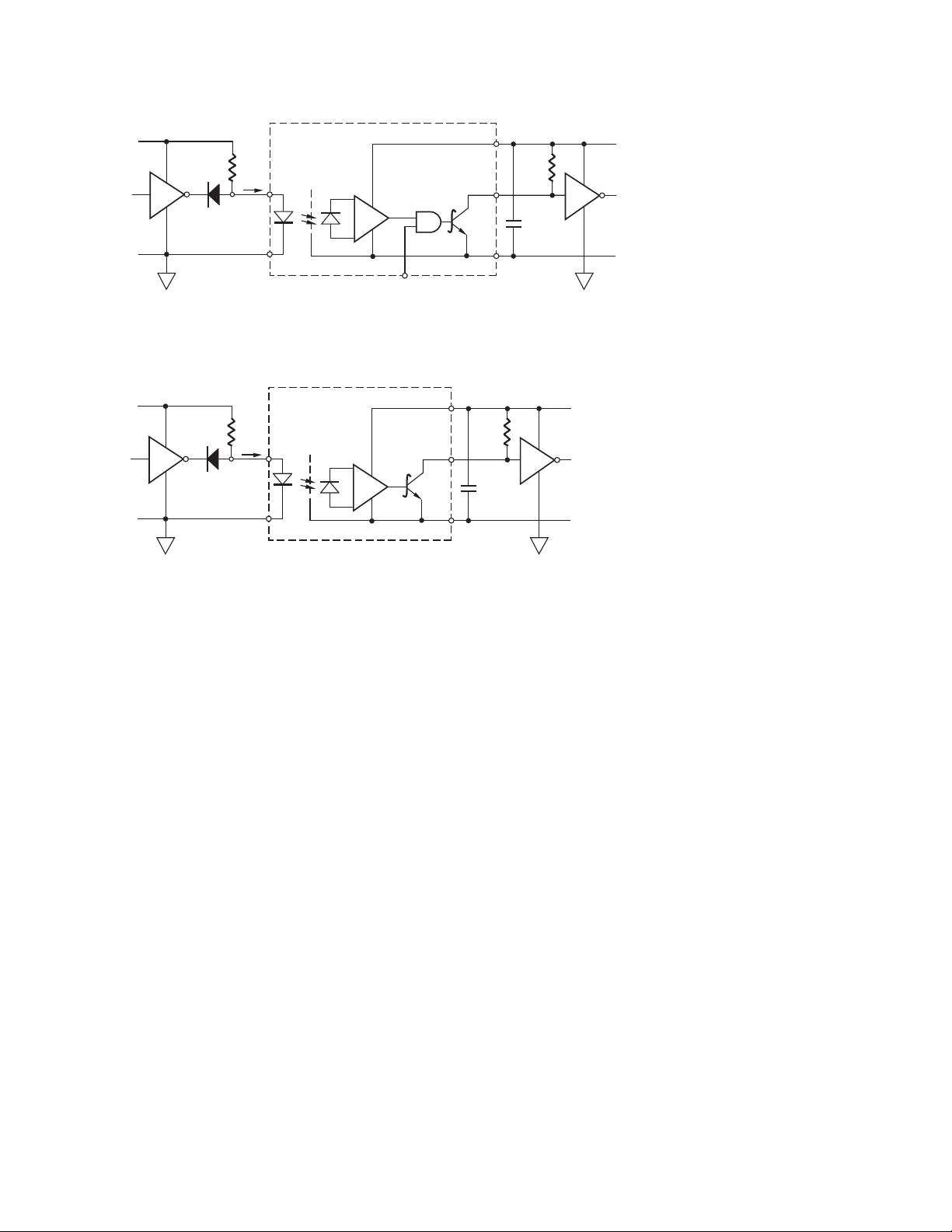
*DIODE D1 (1N916 OR EQUIVALENT) IS NOT REQUIRED FOR UNITS WITH OPEN COLLECTOR OUTPUT.
5 V
V
CC1
470 Ω
GND 1
1
D1*
D1*
I
F
2
+
V
F
3
–
I
F
+
V
F
–
SHIELD
DUAL CHANNEL DEVICE
CHANNEL 1 SHOWN
1
2
SHIELD
V
7
E
8
7
5
390 Ω
0.1 µF
BYPASS
8
6
5
390 Ω
0.1 µF
BYPASS
2
5 V
2
V
CC2
GND 2
5 V
V
CC2
GND 2
Figure 18. Recommended TTL/LSTTL to TTL/LSTTL interface circuit.
20
Page 21
Propagation Delay, Pulse-Width Distortion and Propagation
Delay Skew
Propagation delay is a gure of merit which describes
how quickly a logic signal propagates through a system. The propaga tion delay from low to high (t
) is the
PLH
amount of time required for an input signal to propagate
to the output, causing the output to change from low to
high. Similarly, the propagation delay from high to low
(t
) is the amount of time required for the input signal
PHL
to propagate to the output causing the output to change
from high to low (see Figure 8).
Pulse-width distortion (PWD) results when t
PLH
and t
PHL
di er in value. PWD is de ned as the di erence between t
PLH
and t
and often determines the maximum
PHL
data rate capa bil ity of a transmission system. PWD can
be expressed in percent by dividing the PWD (in ns) by
the minimum pulse width (in ns) being transmitted. Typically, PWD on the order of 20-30% of the minimum pulse
width is tolerable; the exact gure depends on the particular application (RS232, RS422, T-l, etc.).
Propagation delay skew, t
, is an important parameter to
PSK
consider in parallel data appli ca tions where synchronization of signals on parallel data lines is a concern. If the
parallel data is being sent through a group of optocouplers, di er ences in propagation delays will cause the
data to arrive at the outputs of the optocouplers at di erent times. If this di erence in propagation delays is large
enough, it will determine the maximum rate at which
parallel data can be sent through the optocouplers.
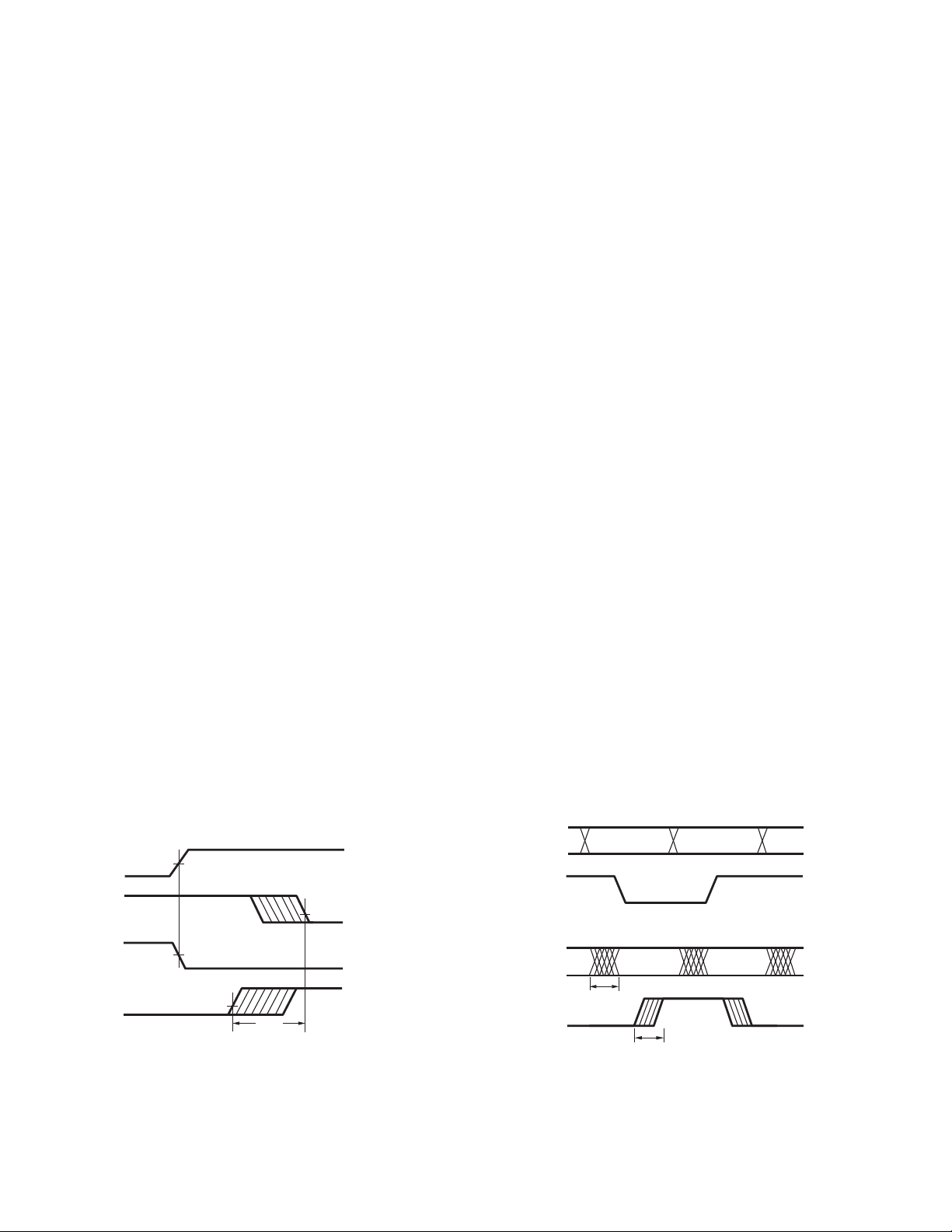
puts of a group of optocouplers are switched either ON
or OFF at the same time, t
the shortest propagation delay, either t
longest propagation delay, either t
As mentioned earlier, t
is the di erence between
PSK
can determine the maximum
PSK
PLH
or t
PLH
or t
PHL
PHL
.
, and the
parallel data transmission rate. Figure 20 is the timing
diagram of a typical parallel data application with both
the clock and the data lines being sent through optocouplers. The gure shows data and clock signals at the
inputs and outputs of the optocouplers. To obtain the
maximum data transmission rate, both edges of the
clock signal are being used to clock the data; if only one
edge were used, the clock signal would need to be twice
as fast.
Propagation delay skew repre sents the uncertainty of
where an edge might be after being sent through an
opto coupler. Figure 20 shows that there will be uncertainty in both the data and the clock lines. It is important
that these two areas of uncertainty not overlap, otherwise the clock signal might arrive before all of the data
outputs have settled, or some of the data outputs may
start to change before the clock signal has arrived. From
these considera tions, the absolute minimum pulse width
that can be sent through optocouplers in a parallel application is twice t
. A cautious design should use a slightly
PSK
longer pulse width to ensure that any additional uncertainty in the rest of the circuit does not cause a problem.
Propagation delay skew is de ned as the di erence between the minimum and maximum propagation delays,
either t
PLH
or t
, for any given group of optocouplers
PHL
which are operating under the same conditions (i.e., the
same drive current, supply voltage, output load, and operating tempera ture). As illustrated in Figure 19, if the in-
I
F
V
O
F
V
O
Figure 19. Illustration of propagation delay skew - t
50%
50%I
1.5 V
t
PSK
1.5 V
.
PSK
The t
speci ed optocouplers o er the advantages of
PSK
guaranteed speci cations for propagation delays, pulsewidth distortion and propagation delay skew over the
recom mended temper a ture, input current, and power
supply ranges.
DATA
INPUTS
CLOCK
DATA
OUTPUTS
CLOCK
Figure 20. Parallel data transmission example.
t
PSK
t
PSK
21
Page 22

For product information and a complete list of distributors, please go to our website: www.avagotech.com
Avago, Avago Technologies, and the A logo are trademarks of Avago Technologies Limited in the United States and other countries.
Data subject to change. Copyright © 2005-2012 Avago Technologies Limited. All rights reserved. Obsoletes AV02-0170EN
AV02-0940EN - February 16, 2012
 Loading...