

Page 1
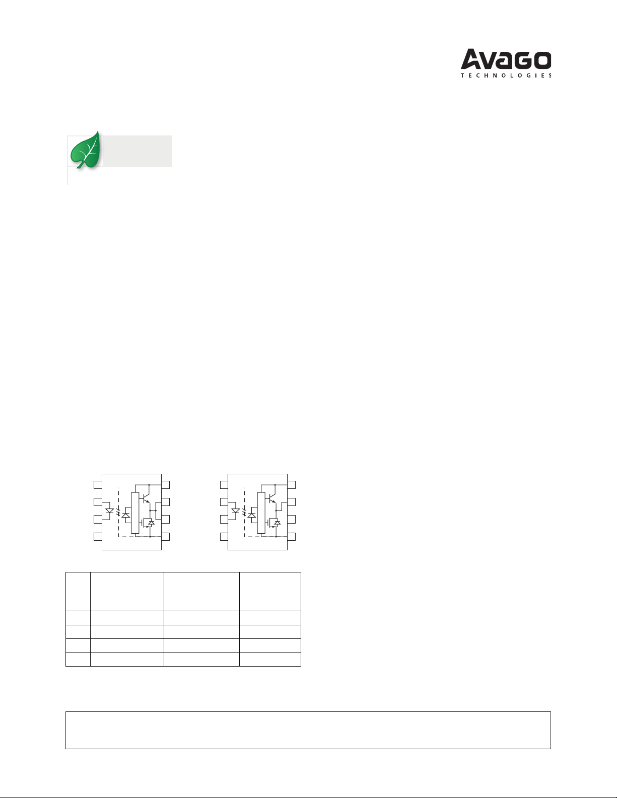
HCPL-3120/J312, HCNW3120
Lead (Pb) Free
RoHS 6 fully
compliant
RoHS 6 fully compliant options available;
-xxxE denotes a lead-free product
1
3
SHIELD
2
4
8
6
7
5
N/C
CATHODE
ANODE
N/C
V
CC
V
O
V
O
V
EE
1
3
SHIELD
2
4
8
6
7
5
N/C
CATHODE
ANODE
N/C
V
CC
N/C
V
O
V
EE
HCNW3120
HCPL-3120/J312
2.5 Amp Output Current IGBT Gate Drive Optocoupler
Data Sheet
Description
The HCPL-3120 contains a GaAsP LED while the HCPLJ312 and the HCNW3120 contain an AlGaAs LED. The LED
is optically coupled to an integrated circuit with a power
output stage. These optocouplers are ideally suited for
driving power IGBTs and MOSFETs used in motor control
inverter applications. The high operating voltage range
of the output stage provides the drive voltages required
by gate controlled devices. The voltage and current
supplied by these optocouplers make them ideally
suited for directly driving IGBTs with ratings up to 1200
V/100 A. For IGBTs with higher ratings, the HCPL-3120
series can be used to drive a discrete power stage which
drives the IGBT gate. The HCNW3120 has the highest insulation voltage of V
= 1414 Vpeak in the IEC/EN/DIN
IORM
EN 60747-5-2. The HCPL-J312 has an insulation voltage
of V
IORM
= 891 V
and the V
peak
IORM
= 630 V
peak
is also
available with the HCPL-3120 (Option 060).
Functional Diagram
TRUTH TABLE
VCC - VEE
“POSITIVE GOING”
LED
(i.e., TURN-ON)
OFF 0 - 30 V 0 - 30 V LOW
ON 0 - 11 V 0 - 9.5 V LOW
ON 11 - 13.5 V 9.5 - 12 V TRANSITION
ON 13.5 - 30 V 12 - 30 V HIGH
VCC - VEE
“NEGATIVE GOING”
(i.e., TURN-OFF) VO
Features
• 2.5 A maximum peak output current
• 2.0 A minimum peak output current
• 25 kV/µs minimum Common Mode Rejection (CMR) at
VCM = 1500 V
• 0.5 V maximum low level output voltage (VOL)
Eliminates need for negative gate drive
• ICC = 5 mA maximum supply current
• Under Voltage Lock-Out protection (UVLO) with
hysteresis
• Wide operating VCC range: 15 to 30 Volts
• 500 ns maximum switching speeds
• Industrial temperature range: -40°C to 100°C
• SafetyApproval:
UL Recognized
3750 Vrms for 1 min. for HCPL-3120/J312
5000 Vrms for 1 min. for HCNW3120
CSA Approval
IEC/EN/DIN EN 60747-5-2 Approved
V
V
V
IORM
IORM
IORM
= 630 V
= 891 V
= 1414 V
for HCPL-3120 (Option 060)
peak
for HCPL-J312
peak
for HCNW3120
peak
Applications
• IGBT/MOSFET gate drive
• AC/Brushless DC motor drives
• Industrial inverters
• Switch mode power supplies
A 0.1 µF bypass capacitor must be connected between pins 5 and 8.
CAUTION: It is advised that normal static precautions be taken in handling and assembly
of this component to prevent damage and/or degradation which may be induced by ESD.
Page 2

Selection Guide
Part Number HCPL-3120 HCPL-J312 HCNW3120 HCPL-3150*
Output Peak Current ( I
IEC/EN/DIN EN V
60747-5-2 Approval (Option 060) (Option 060)
*The HCPL-3150 Data sheet available. Contact Avago sales representative or authorized distributor.
) 2.5 A 2.5 A 2.5 A 0.6 A
O
IORM
= 630 V
peak
V
IORM
= 891 V
peak
V
IORM
= 1414 V
peak
V
IORM
= 630 V
peak
Ordering Information
HCPL-3120 and HCPL-J312 are UL recognized with 3750 Vrms for 1 minute per UL1577. HCNW3120 is UL Recognized
with 5000 Vrms for 1 minute per UL1577.
Option
Part RoHS Non RoHS Surface Gull Tape IEC/EN/DIN
Number Compliant Compliant Package Mount Wing & Reel EN 60747-5-2 Quantity
-000E No option 50 per tube
-300E #300 X X 50 per tube
HCPL-3120 -500E #500 X X X 1000 per reel
-060E #060 X 50 per tube
-360E #360 X X X 50 per tube
-560E #560 X X X X 1000 per tube
-000E No option X 50 per tube
HCPL-J312 -300E #300 X X X 50 per tube
-500E #500 X X X X 1000 per reel
-000E No option X 42 per tube
HCNW3120 -300E #300 X X X 42 per tube
-500E #500 X X X X 750 per reel
300mil
DIP-8
300mil
DIP-8
400mil
DIP-8
To order, choose a part number from the part number column and combine with the desired option from the option
column to form an order entry.
Example 1:
HCPL-3120-560E to order product of 300 mil DIP Gull Wing Surface Mount package in Tape and Reel packaging with
IEC/EN/DIN EN 60747-5-2 Safety Approval in RoHS compliant.
Example 2:
HCPL-3120 to order product of 300 mil DIP package in tube packaging and non RoHS compliant.
Option datasheets are available. Contact your Avago sales representative or authorized distributor for information.
Remarks: The notation ‘#XXX’ is used for existing products, while (new) products launched since 15th July 2001 and
RoHS compliant option will use ‘-XXXE’.
2
Page 3
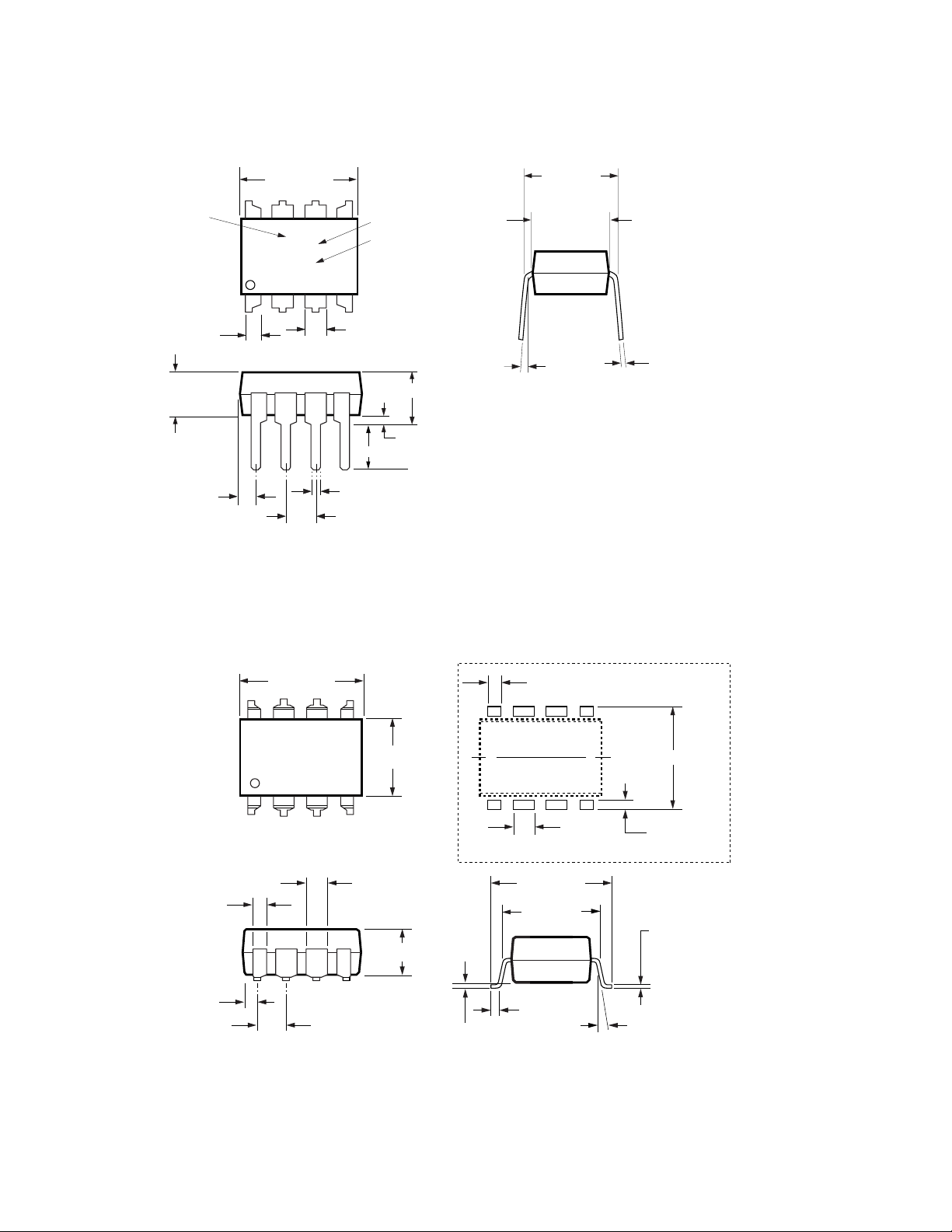
Package Outline Drawings
1.080 ± 0.320
(0.043 ± 0.013)
2.54 ± 0.25
(0.100 ± 0.010)
0.51 (0.020) MIN.
0.65 (0.025) MAX.
4.70 (0.185) MAX.
2.92 (0.115) MIN.
5° TYP.
0.254
+ 0.076
- 0.051
(0.010
+ 0.003)
- 0.002)
7.62 ± 0.25
(0.300 ± 0.010)
6.35 ± 0.25
(0.250 ± 0.010)
9.65 ± 0.25
(0.380 ± 0.010)
1.78 (0.070) MAX.
1.19 (0.047) MAX.
A XXXXZ
YYWW
DATE CODE
DIMENSIONS IN MILLIMETERS AND (INCHES).
5678
4321
OPTION CODE*
TYPE NUMBER
* MARKING CODE LETTER FOR OPTION NUMBERS.
"V" = OPTION 060
OPTION NUMBERS 300 AND 500 NOT MARKED.
NOTE: FLOATING LEAD PROTRUSION IS 0.25 mm (10 mils) MAX.
3.56 ± 0.13
(0.140 ± 0.005)
0.635 ± 0.25
(0.025 ± 0.010)
12° NOM.
9.65 ± 0.25
(0.380 ± 0.010)
0.635 ± 0.130
(0.025 ± 0.005)
7.62 ± 0.25
(0.300 ± 0.010)
5
6
7
8
4
3
2
1
9.65 ± 0.25
(0.380 ± 0.010)
6.350 ± 0.25
(0.250 ± 0.010)
1.016 (0.040)
1.27 (0.050)
10.9 (0.430)
2.0 (0.080)
LAND PATTERN RECOMMENDATION
1.080 ± 0.320
(0.043 ± 0.013)
3.56 ± 0.13
(0.140 ± 0.005)
1.780
(0.070)
MAX.
1.19
(0.047)
MAX.
2.54
(0.100)
BSC
DIMENSIONS IN MILLIMETERS (INCHES).
LEAD COPLANARITY = 0.10 mm (0.004 INCHES).
NOTE: FLOATING LEAD PROTRUSION IS 0.25 mm (10 mils) MAX.
0.254
+ 0.076
- 0.051
(0.010
+ 0.003)
- 0.002)
HCPL-3120 Outline Drawing (Standard DIP Package)
HCPL-3120 Gull Wing Surface Mount Option 300 Outline Drawing
3
Page 4
1.080 ± 0.320
(0.043 ± 0.013)
2.54 ± 0.25
(0.100 ± 0.010)
0.51 (0.020) MIN.
0.65 (0.025) MAX.
4.70 (0.185) MAX.
2.92 (0.115) MIN.
5° TYP.
0.254
+ 0.076
- 0.051
(0.010
+ 0.003)
- 0.002)
7.62 ± 0.25
(0.300 ± 0.010)
6.35 ± 0.25
(0.250 ± 0.010)
9.80 ± 0.25
(0.386 ± 0.010)
1.78 (0.070) MAX.
1.19 (0.047) MAX.
A XXXX
YYWW
DATE CODE
DIMENSIONS IN MILLIMETERS AND (INCHES).
5678
4321
TYPE NUMBER
OPTION NUMBERS 300 AND 500 NOT MARKED.
NOTE: FLOATING LEAD PROTRUSION IS 0.25 mm (10 mils) MAX.
3.56 ± 0.13
(0.140 ± 0.005)
0.635 ± 0.25
(0.025 ± 0.010)
12°NOM.
9.65 ± 0.25
(0.380 ± 0.010)
0.635 ± 0.130
(0.025 ± 0.005)
7.62 ± 0.25
(0.300 ± 0.010)
5
6
7
8
4
3
2
1
9.80 ± 0.25
(0.386 ± 0.010)
6.350 ± 0.25
(0.250 ± 0.010)
1.016 (0.040)
1.27 (0.050)
10.9 (0.430)
2.0 (0.080)
LAND PATTERN RECOMMENDATION
1.080 ± 0.320
(0.043 ± 0.013)
3.56 ± 0.13
(0.140 ± 0.005)
1.780
(0.070)
MAX.
1.19
(0.047)
MAX.
2.54
(0.100)
BSC
DIMENSIONS IN MILLIMETERS (INCHES).
LEAD COPLANARITY = 0.10 mm (0.004 INCHES).
NOTE: FLOATING LEAD PROTRUSION IS 0.5 mm (20 mils) MAX.
0.254
+ 0.076
- 0.051
(0.010
+ 0.003)
- 0.002)
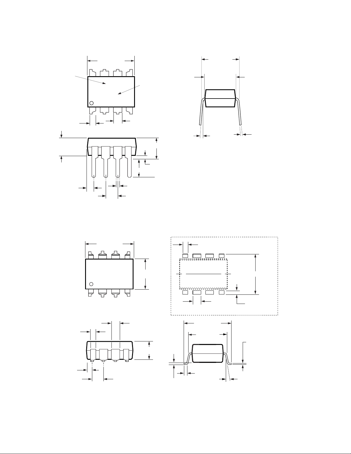
Package Outline Drawings
HCPL-J312 Outline Drawing (Standard DIP Package)
HCPL-J312 Gull Wing Surface Mount Option 300 Outline Drawing
4
Page 5
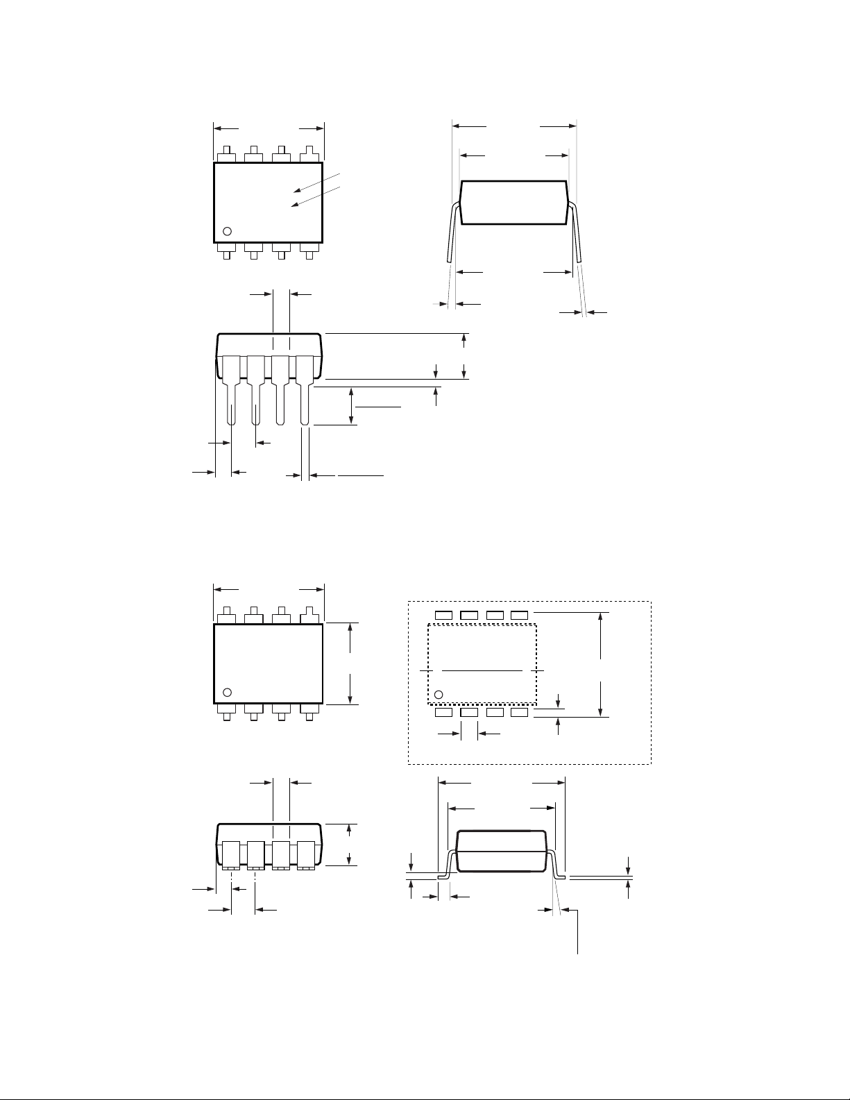
HCNW3120 Outline Drawing (8-Pin Wide Body Package)
5
6
7
8
4
3
2
1
11.15 ± 0.15
(0.442 ± 0.006)
1.78 ± 0.15
(0.070 ± 0.006)
5.10
(0.201)
MAX.
1.55
(0.061)
MAX.
2.54 (0.100)
TYP.
DIMENSIONS IN MILLIMETERS (INCHES).
NOTE: FLOATING LEAD PROTRUSION IS 0.25 mm (10 mils) MAX.
7° TYP.
0.254
+ 0.076
- 0.0051
(0.010
+ 0.003)
- 0.002)
11.00
(0.433)
9.00 ± 0.15
(0.354 ± 0.006)
MAX.
10.16 (0.400)
TYP.
A
HCNWXXXX
YYWW
DATE CODE
TYPE NUMBER
0.51 (0.021) MIN.
0.40 (0.016)
0.56 (0.022)
3.10 (0.122)
3.90 (0.154)
1.00 ± 0.15
(0.039 ± 0.006)
7° NOM.
12.30 ± 0.30
(0.484 ± 0.012)
0.75 ± 0.25
(0.030 ± 0.010)
11.00
(0.433)
5
6
7
8
4
3
2
1
11.15 ± 0.15
(0.442 ± 0.006)
9.00 ± 0.15
(0.354 ± 0.006)
1.3
(0.051)
13.56
(0.534)
2.29
(0.09)
LAND PATTERN RECOMMENDATION
1.78 ± 0.15
(0.070 ± 0.006)
4.00
(0.158)
MAX.
1.55
(0.061)
MAX.
2.54
(0.100)
BSC
DIMENSIONS IN MILLIMETERS (INCHES).
LEAD COPLANARITY = 0.10 mm (0.004 INCHES).
NOTE: FLOATING LEAD PROTRUSION IS 0.25 mm (10 mils) MAX.
0.254
+ 0.076
- 0.0051
(0.010
+ 0.003)
- 0.002)
MAX.
HCNW3120 Gull Wing Surface Mount Option 300 Outline Drawing
5
Page 6
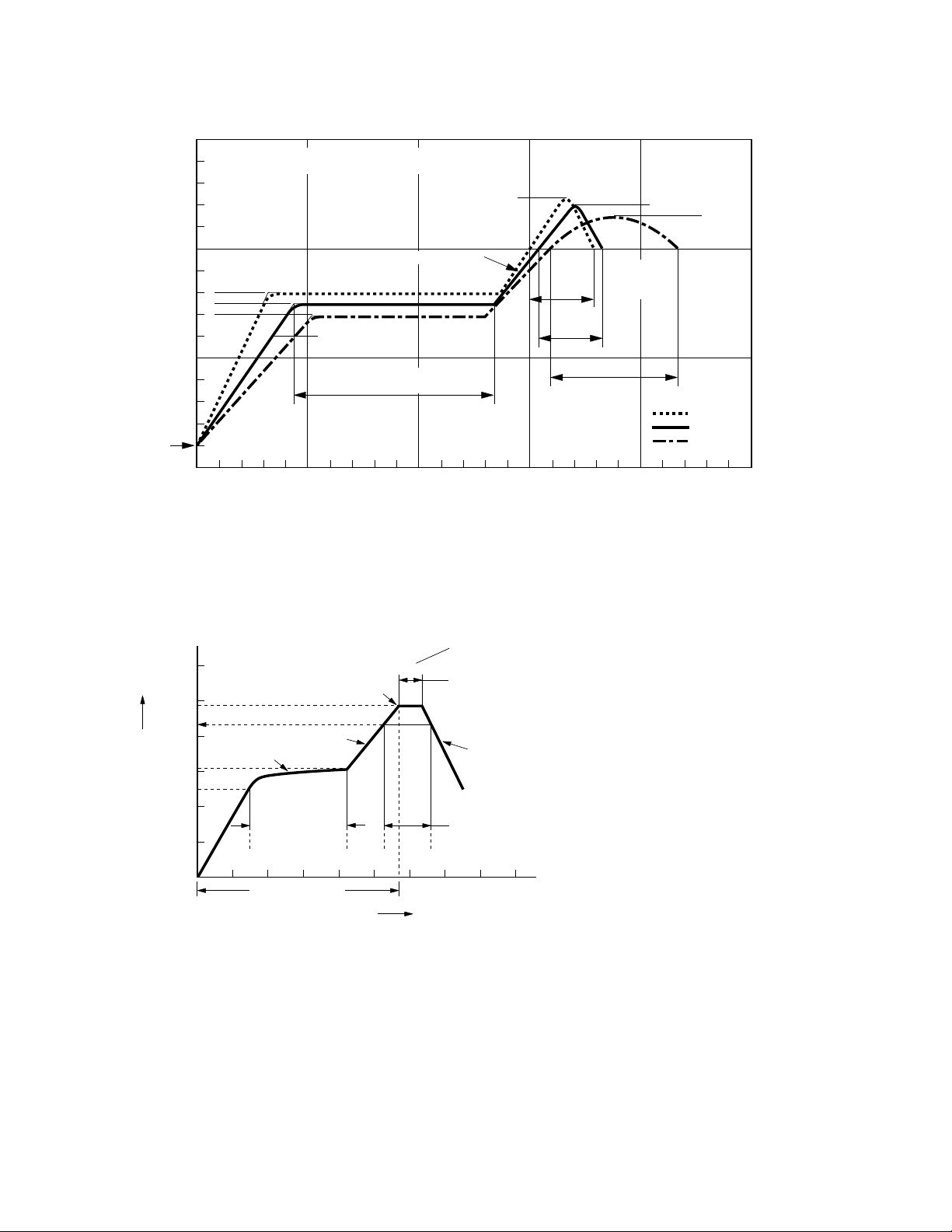
Solder Reow Temperature Prole
0
TIME (SECONDS)
TEMPERATURE (°C)
200
100
50 150100 200 250
300
0
30
SEC.
50 SEC.
30
SEC.
160 °C
140 °C
150 °C
PEAK
TEMP.
245 °C
PEAK
TEMP.
240 °C
PEAK
TEMP.
230 °C
SOLDERING
TIME
200 °C
PREHEATING TIME
150 °C, 90 + 30 SEC.
2.5 C ± 0.5 °C/SEC.
3 °C + 1 °C/–0.5 °C
TIGHT
TYPICAL
LOOSE
ROOM
TEMPERATURE
PREHEATING RATE 3 °C + 1 °C/–0.5 °C/SEC.
REFLOW HEATING RATE 2.5 °C ± 0.5 °C/SEC.
NOTE: NON-HALIDE FLUX SHOULD BE USED.
217 °C
RAMP-DOWN
6 °C/SEC. MAX.
RAMP-UP
3 °C/SEC. MAX.
150 - 200 °C
* 260 +0/-5 °C
t 25 °C to PEAK
60 to 150 SEC.
15 SEC.
TIME WITHIN 5 °C of ACTUAL
PEAK TEMPERATURE
t
p
t
s
PREHEAT
60 to 180 SEC.
t
L
T
L
T
smax
T
smin
25
T
p
TIME
TEMPERATURE
NOTES:
THE TIME FROM 25 °C to PEAK TEMPERATURE = 8 MINUTES MAX.
T
smax
= 200 °C, T
smin
= 150 °C
NOTE: NON-HALIDE FLUX SHOULD BE USED.
* RECOMMENDED PEAK TEMPERATURE FOR WIDEBODY 400mils PACKAGE IS 245 °C
Recommended Pb-Free IR Prole
6
Page 7

Regulatory Information
Agency/Standard HCPL-3120 HCPL-J312 HCNW3120
Underwriters Laboratory (UL) Compliant Compliant Compliant
Recognized under UL 1577, Component Recognition Program,
Category, File E55361
Canadian Standards Association (CSA) File CA88324, Compliant Compliant Compliant
per Component Acceptance Notice #5
IEC/EN/DIN EN 60747-5-2 Compliant Compliant Compliant
Option 060
Insulation and Safety Related Specications
Value
HCPL- HCPL- HCNW
Parameter Symbol 3120 J312 3120 Units Conditions
Minimum External L(101) 7.1 7.4 9.6 mm Measured from input terminals to output
Air Gap (Clearance) terminals, shortest distance through air.
Minimum External L(102) 7.4 8.0 10.0 mm Measured from input terminals to output
Tracking (Creepage) terminals, shortest distance path along
body.
Minimum Internal 0.08 0.5 1.0 mm Insulation thickness between emitter
Plastic Gap and detector; also known as distance
(Internal Clearance) through insulation.
Tracking Resistance CTI >175 >175 >200 Volts DIN IEC 112/VDE 0303 Part 1
(Comparative
Tracking Index)
Isolation Group IIIa IIIa IIIa Material Group (DIN VDE 0110, 1/89,
Table 1)
7
Page 8

All Avago data sheets report the creepage and clearance
inherent to the optocoupler component itself. These
dimensions are needed as a starting point for the
equipment designer when determining the circuit insulation requirements. However, once mounted on a printed
circuit board, minimum creep-age and clearance requirements must be met as specied for individual equipment
the surface of a printed circuit board between the solder
llets of the input and output leads must be considered.
There are recommended techniques such as grooves
and ribs which may be used on a printed circuit board
to achieve desired creepage and clearances. Creepage
and clearance distances will also change depending on
factors such as pollution degree and insulation level.
standards. For creepage, the shortest distance path along
IEC/EN/DIN EN 60747-5-2 Insulation Related Characteristics
HCPL-3120
Description Symbol Option 060 HCPL-J312 HCNW3120 Unit
Installation classication per DIN VDE 0110/1.89,
Table 1
for rated mains voltage ≤150 V rms I-IV I-IV I-IV
for rated mains voltage ≤300 V rms I-IV I-IV I-IV
for rated mains voltage ≤450 V rms I-III I-III I-IV
for rated mains voltage ≤600 V rms I-III I-IV
for rated mains voltage ≤1000 V rms I-III
Climatic Classication 55/100/21 55/100/21 55/100/21
Pollution Degree (DIN VDE 0110/1.89) 2 2 2
Maximum Working Insulation Voltage V
Input to Output Test Voltage, Method b* VPR 1181 1670 2652 V
V
x 1.875 = VPR, 100% Production Test,
IORM
tm = 1 sec, Partial Discharge < 5pC
Input to Output Test Voltage, Method a* VPR 945 1336 2121 V
V
x 1.5 = VPR, Type and Sample Test,
IORM
tm = 60 sec, Partial Discharge < 5pC
Highest Allowable Overvoltage* V
(Transient Overvoltage, t
= 10 sec)
ini
Safety Limiting Values – maximum values allowed
in the event of a failure, also see Figure 37.
Case Temperature TS 175 175 150 °C
Input Current I
Output Power P
Insulation Resistance at TS, VIO = 500 V RS ≥109 ≥109 ≥109 Ω
630 891 1414 V
IORM
6000 6000 8000 V
IOTM
230 400 400 mA
S INPUT
600 600 700 mW
S OUTPUT
peak
peak
peak
peak
*Refer to the IEC/EN/DIN EN 60747-5-2 section (page 1-6/8) of the Isolation Control Component Designer’s Catalog for a detailed description of
Method a/b partial discharge test proles.
Note: These optocouplers are suitable for “safe electrical isolation” only within the safety limit data. Maintenance of the safety data shall be ensured by means of protective circuits. Surface mount classication is Class A in accordance with CECC 00802.
8
Page 9

Absolute Maximum Ratings
Parameter Symbol Min. Max. Units Note
Storage Temperature TS -55 125 °C
Operating Temperature TA -40 100 °C
Average Input Current I
Peak Transient Input Current I
(<1 µs pulse width, 300 pps)
Reverse Input Voltage HCPL-3120 VR 5 Volts
HCPL-J312 5
HCNW3120
“High” Peak Output Current I
“Low” Peak Output Current I
Supply Voltage (VCC - VEE) 0 35 Volts
Input Current (Rise/Fall Time) t
Output Voltage V
Output Power Dissipation PO 250 mW 3
Total Power Dissipation PT 295 mW 4
Lead Solder Temperature HCPL-3120 260°C for 10 sec., 1.6 mm below seating plane
HCPL-J312
HCNW3120 260°C for 10 sec., up to seating plane
Solder Reow Temperature Prole See Package Outline Drawings section
25 mA 1
F(AVG)
1.0 A
F(TRAN)
2.5 A 2
OH(PEAK)
2.5 A 2
OL(PEAK)
r(IN) /tf(IN)
0 VCC Volts
O(PEAK)
500 ns
Recommended Operating Conditions
Parameter Symbol Min. Max. Units
Power Supply Voltage (VCC - VEE) 15 30 Volts
Input Current (ON) HCPL-3120 7
HCPL-J312 I
HCNW3120 10
Input Voltage (OFF) V
Operating Temperature TA -40 100 °C
16 mA
F(ON)
-3.6 0.8 V
F(OFF)
9
Page 10

Electrical Specications (DC)
Over recommended operating conditions (TA = -40 to 100°C, for HCPL-3120, HCPL-J312 I
HCNW3120 I
= 10 to 16mA, V
F(ON)
= -3.6 to 0.8 V, VCC = 15 to 30 V, VEE = Ground) unless otherwise specied.
F(OFF)
= 7 to 16mA, for
F(ON)
Parameter Symbol Device Min. Typ.* Max. Units Test Conditions Fig. Note
High Level Output I
Current
2.0 A VO = (VCC - 15 V)
Low Level Output I
Current
2.0 A VO = (VEE + 15 V)
OH
OL
High Level Output VOH (V
Voltage 19
Low Level Output V
OL
Voltage 20
High Level Supply I
CCH
Current IF = 7 to 16 mA
Low Level Supply I
2.5 5.0 mA Output Open,
CCL
Current VF = -3.0 to +0.8 V
Threshold Input I
Current Low to
High
HCNW3120 2.3 8.0
HCPL-J312 1.0
Threshold Input V
HCPL-3120 2.3 5.0 mA IO = 0 mA, 9, 15,
FLH
FHL
Voltage High to
Low
Input Forward VF HCPL-3120 1.2 1.5 1.8 V IF = 10 mA 16
Voltage
HCPL-J312 1.6 1.95
HCNW3120
Temperature ∆VF/∆TA HCPL-3120 -1.6 mV/°C IF = 10 mA
Coecient of
Forward Voltage
HCPL-J312 -1.3
HCNW3120
Input Reverse BVR HCPL-3120 5 V IR = 10 µA
Breakdown
Voltage
HCPL-J312 3 IR = 100 µA
HCNW3120
Input Capacitance CIN HCPL-3120 60 pF f = 1 MHz,
HCPL-J312 70
HCNW3120
UVLO Threshold V
UVLO+
IF = 10 mA 34
V
UVLO–
UVLO Hysteresis UVLO
0.5 1.5 A VO = (VCC - 4 V) 2, 3, 5
17
0.5 2.0 A VO = (VEE + 2.5 V) 5, 6, 5
18
- 4) (V
CC
- 3) V IO = -100 mA 1, 3, 6, 7
CC
0.1 0.5 V IO = 100 mA 4, 6,
2.5 5.0 mA Output Open, 7, 8
VO > 5 V 21
0.8 V
VF = 0 V
11.0 12.3 13.5 V VO > 5 V, 22,
9.5 10.7 12.0
1.6
HYS
2
2
*All typical values at TA = 25°C and VCC - VEE = 30 V, unless otherwise noted.
10
Page 11

Switching Specications (AC)
Over recommended operating conditions (TA = -40 to 100°C, for HCPL-3120,HCPL-J312 I
HCNW3120 I
= 10 to 16mA, V
F(ON)
= -3.6 to 0.8 V, VCC = 15 to 30 V, VEE = Ground) unless otherwise specied.
F(OFF)
= 7 to 16mA, for
F(ON)
Parameter Symbol Min. Typ.* Max. Units Test Conditions Fig. Note
Propagation Delay Time t
to High Output Level Cg = 10 nF, 12, 13,
Propagation Delay Time t
to Low Output Level
Pulse Width Distortion PWD 0.3 µs 17
Propagation Delay PDD -0.35 0.35 µs 35, 36 12
Dierence Between Any (t
Two Parts
Rise Time tr 0.1 µs 23
Fall Time tf 0.1 µs
UVLO Turn On Delay t
UVLO Turn O Delay t
Output High Level Common |CMH| 25 35 kV/µs TA = 25°C, 24 13, 14
Mode Transient Immunity IF = 10 to 16 mA,
VCM = 1500 V,
VCC = 30 V
Output Low Level Common |CML| 25 35 kV/µs TA = 25°C, 13, 15
Mode Transient Immunity VCM = 1500 V,
VF = 0 V, VCC = 30 V
0.10 0.30 0.50 µs Rg = 10 Ω, 10, 11, 16
PLH
0.10 0.30 0.50 µs
PHL
f = 10 kHz, 14, 23
Duty Cycle = 50%
- t
PHL
UVLO ON
UVLO OFF
)
PLH
0.8 µs VO > 5 V, IF = 10 mA 22
0.6 VO < 5 V, IF = 10 mA
*All typical values at TA = 25°C and VCC - VEE = 30 V, unless otherwise noted.
11
Page 12

Package Characteristics
Over recommended temperature (TA = -40 to 100°C) unless otherwise specied.
Parameter Symbol Device Min. Typ. Max. Units Test Conditions Fig. Note
Input-Output Momentary V
Withstand Voltage**
HCPL-J312 3750
HCNW3120 5000
Resistance R
(Input-Output) HCPL-J312
HCNW3120 1012 1013 TA = 25°C
10
Capacitance C
(Input-Output) HCPL-J312 0.8
HCNW3120 0.5 0.6
LED-to-Case Thermal qLC 467 °C/W Thermocouple 28
Resistance located at center
LED-to-Detector Thermal qLD 442 °C/W underside of
Resistance package
Detector-to-Case qDC 126 °C/W
Thermal Resistance
HCPL-3120 3750 V
ISO
RH < 50%, 8, 11
RMS
t = 1 min.,
TA = 25°C
HCPL-3120 1012 Ω V
I-O
11
TA = 100°C
HCPL-3120 0.6 pF f = 1 MHz
I-O
I-O
9, 11
10, 11
= 500 V
DC
11
*All typicals at TA = 25°C.
**The Input-Output Momentary Withstand Voltage is a dielectric voltage rating that should not be interpreted as an input-output continuous
voltage rating. For the continuous voltage rating refer to your equipment level safety specication or Avago Application Note 1074 entitled “Optocoupler Input-Output Endurance Voltage.”
Notes:
1. Derate linearly above 70°C free-air temperature at a rate of 0.3 mA/°C.
2. Maximum pulse width = 10 µs, maximum duty cycle = 0.2%. This value is intended to allow for component tolerances for designs with IO peak
minimum = 2.0 A. See Applications section for additional details on limiting IOH peak.
3. Derate linearly above 70°C free-air temperature at a rate of 4.8 mW/°C.
4. Derate linearly above 70°C free-air temperature at a rate of 5.4 mW/°C. The maximum LED junction tem-perature should not exceed 125°C.
5. Maximum pulse width = 50 µs, maximum duty cycle = 0.5%.
6. In this test VOH is measured with a dc load current. When driving capacitive loads VOH will approach VCC as IOH approaches zero amps.
7. Maximum pulse width = 1 ms, maximum duty cycle = 20%.
8. In accordance with UL1577, each optocoupler is proof tested by applying an insulation test voltage ≥4500 Vrms for 1 second (leakage detection current limit, I
9. In accordance with UL1577, each optocoupler is proof tested by applying an insulation test voltage ≥4500 Vrms for 1 second (leakage detection current limit, I
10. In accordance with UL1577, each optocoupler is proof tested by applying an insulation test voltage ≥6000 Vrms for 1 second (leakage detection current limit, I
11. Device considered a two-terminal device: pins 1, 2, 3, and 4 shorted together and pins 5, 6, 7, and 8 shorted together.
12. The dierence between t
13. Pins 1 and 4 need to be connected to LED common.
14. Common mode transient immunity in the high state is the maximum tolerable dVCM/dt of the common mode pulse, VCM, to assure that the
output will remain in the high state (i.e., VO > 15.0 V ).
15. Common mode transient immunity in a low state is the maximum tolerable dVCM/dt of the common mode pulse, VCM, to assure that the output will remain in a low state (i.e., VO < 1.0 V ).
16. This load condition approximates the gate load of a 1200 V/75A IGBT.
17. Pulse Width Distortion (PWD) is dened as |t
≤ 5 µA).
I-O
≤ 5 µA).
I-O
≤ 5 µA).
I-O
PHL
and t
between any two HCPL-3120 parts under the same test condition.
PLH
| for any given device.
PHL-tPLH
12
Page 13
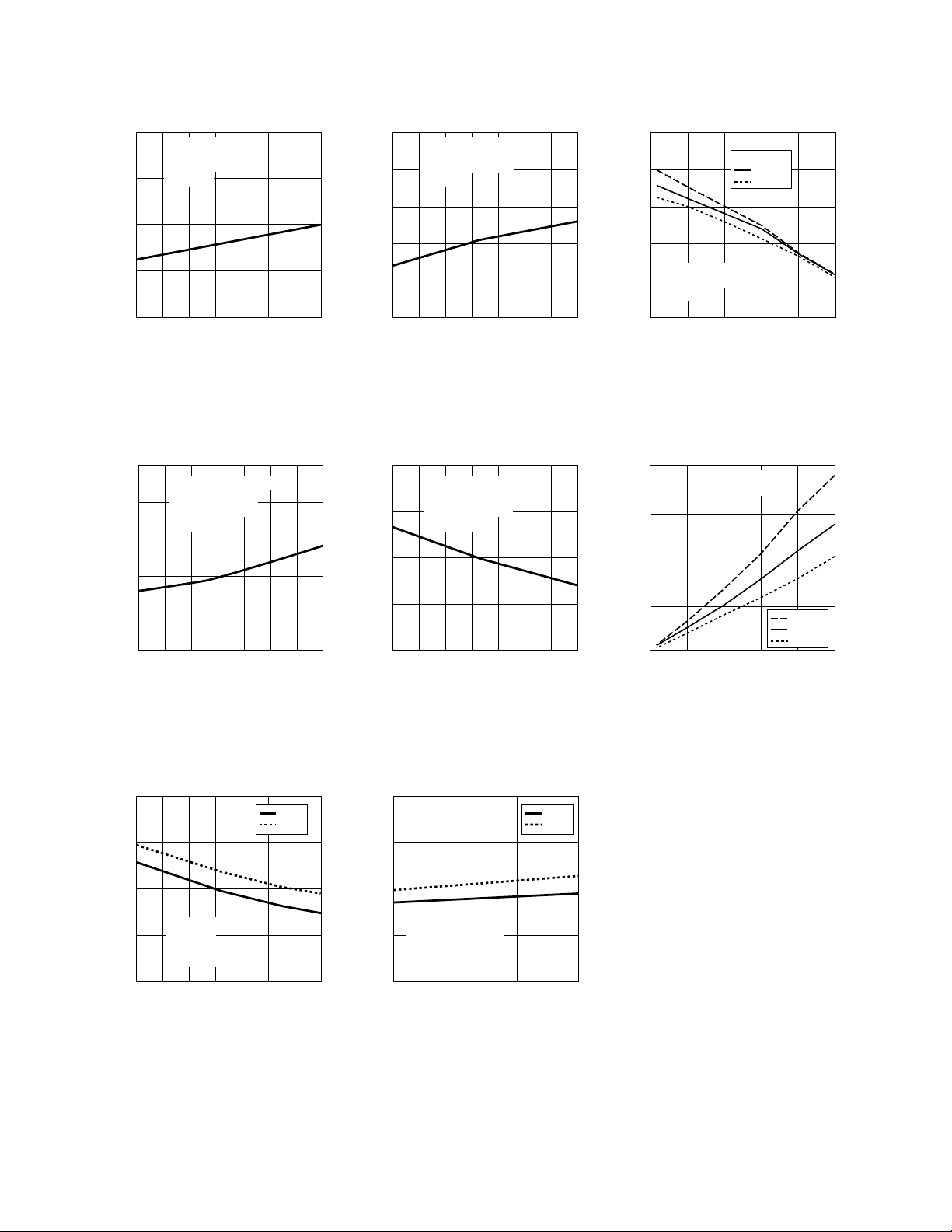
Figure 1. VOH vs. temperature.
(V
OH
– V
CC
) – HIGH OUTPUT VOLTAGE DROP – V
-40
-4
TA – TEMPERATURE – °C
100
-1
-2
-2000 20 40-360 80
IF = 7 to 16 mA
I
OUT
= -100 mA
VCC = 15 to 30 V
VEE = 0 V
I
OH
– OUTPUT HIGH CURRENT – A
-40
1.0
TA – TEMPERATURE – °C
100
1.8
1.6
-20
2.0
0 20 40
1.2
60 80
IF = 7 to 16 mA
V
OUT
= (VCC - 4 V)
VCC = 15 to 30 V
VEE = 0 V
1.4
(V
OH
– V
CC
) – OUTPUT HIGH VOLTAGE DROP – V
0
-6
IOH – OUTPUT HIGH CURRENT – A
2.5
-2
-3
0.5-11.0 1.5-52.0
IF = 7 to 16 mA
VCC = 15 to 30 V
VEE = 0 V
-4
100 °C
25 °C
-40 °C
V
OL
– OUTPUT LOW VOLTAGE – V
-40
0
TA – TEMPERATURE – °C
-20
0.25
0 20
0.05
100
0.15
0.20
0.10
40 60 80
VF (OFF) = -3.0 TO 0.8 V
I
OUT
= 100 mA
VCC = 15 TO 30 V
VEE = 0 V
I
OL
– OUTPUT LOW CURRENT – A
-40
0
TA – TEMPERATURE – °C
-2040 20
1
100
2
3
40 60 80
VF (OFF) = -3.0 TO 0.8 V
V
OUT
= 2.5 V
VCC = 15 TO 30 V
VEE = 0 V
V
OL
– OUTPUT LOW VOLTAGE – V
0
0
IOL – OUTPUT LOW CURRENT – A
2.5
3
0.541.0 1.512.0
V
F(OFF)
= -3.0 to 0.8 V
VCC = 15 to 30 V
VEE = 0 V
2
100 °C
25 °C
-40 °C
I
CC
– SUPPLY CURRENT – mA
-40
1.5
TA – TEMPERATURE – °C
100
3.0
2.5
-20
3.5
0 20 40
2.0
60 80
VCC = 30 V
VEE = 0 V
IF = 10 mA for I
CCH
IF = 0 mA for I
CCL
I
CCH
I
CCL
I
CC
– SUPPLY CURRENT – mA
15
1.5
VCC – SUPPLY VOLTAGE – V
30
3.0
2.5
3.5
20
2.0
25
IF = 10 mA for I
CCH
IF = 0 mA for I
CCL
TA = 25 °C
VEE = 0 V
I
CCH
I
CCL
Figure 2. IOH vs. temperature.
Figure 3. VOH vs. IOH.
Figure 4. V
Figure 7. ICC vs. temperature. Figure 8. ICC vs. VCC.
13
vs. temperature. Figure 5. IOL vs. temperature. Figure 6. VOL vs. IOL.
OL
Page 14
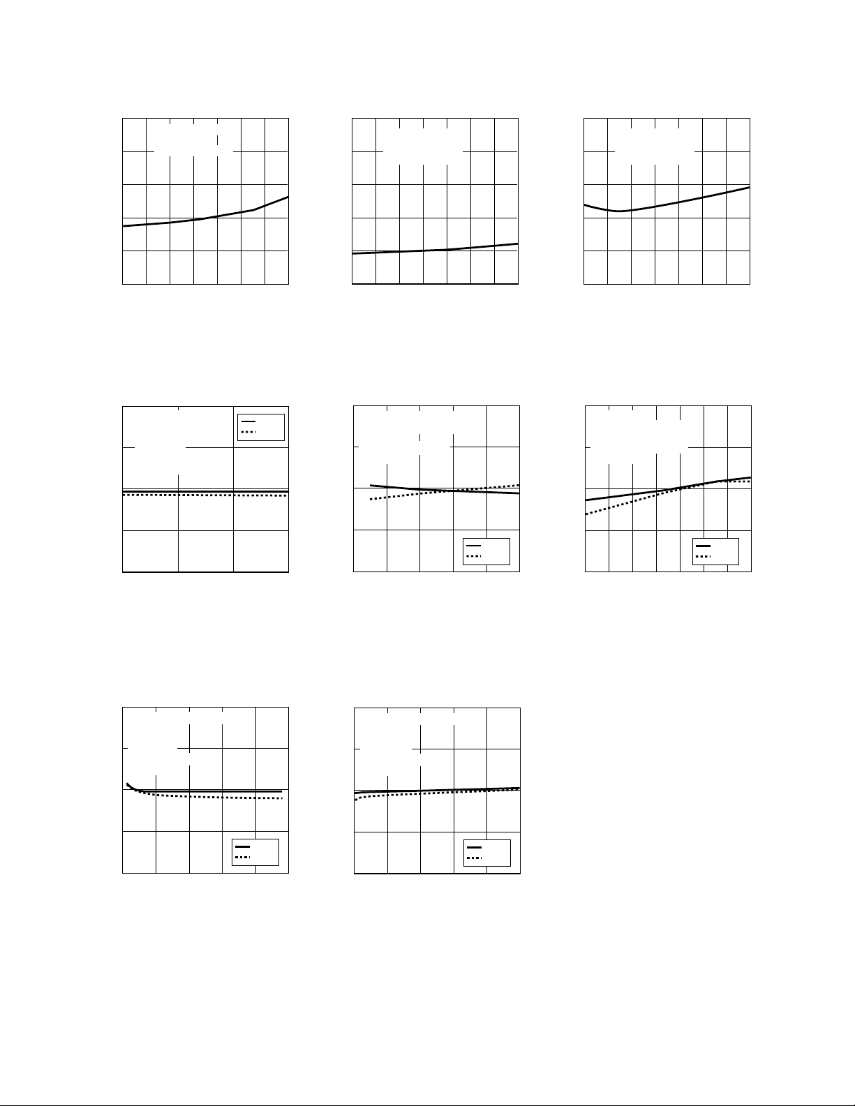
Figure 9. I
I
FLH
– LOW TO HIGH CURRENT THRESHOLD – mA
-40
0
TA – TEMPERATURE – °C
100
3
2
-2040 20 40160 80
5
VCC = 15 TO 30 V
VEE = 0 V
OUTPUT = OPEN
HCPL-3120
I
FLH
– LOW TO HIGH CURRENT THRESHOLD – mA
-40
0
TA – TEMPERATURE – °C
-2050 20
1
100
2
3
40 60 80
VCC = 15 TO 30 V
VEE = 0 V
OUTPUT = OPEN
4
HCPL-J312
I
FLH
– LOW TO HIGH CURRENT THRESHOLD – mA
-40
0
TA – TEMPERATURE – °C
-2050 20
1
100
2
3
40 60 80
VCC = 15 TO 30 V
VEE = 0 V
OUTPUT = OPEN
4
HCNW3120
T
p
– PROPAGATION DELAY – ns
15
100
VCC – SUPPLY VOLTAGE – V
30
400
300
500
20
200
25
IF = 10 mA
TA = 25 °C
Rg = 10 Ω
Cg = 10 nF
DUTY CYCLE = 50%
f = 10 kHz
T
PLH
T
PHL
T
p
– PROPAGATION DELAY – ns
6
100
IF – FORWARD LED CURRENT – mA
16
400
300
500
10
200
12
VCC = 30 V, VEE = 0 V
Rg = 10 Ω, Cg = 10 nF
TA = 25 °C
DUTY CYCLE = 50%
f = 10 kHz
T
PLH
T
PHL
148
T
p
– PROPAGATION DELAY – ns
-40
100
TA – TEMPERATURE – °C
100
400
300
-20
500
0 20 40
200
60 80
T
PLH
T
PHL
IF = 10 mA
VCC = 30 V, VEE = 0 V
Rg = 10 Ω, Cg = 10 nF
DUTY CYCLE = 50%
f = 10 kHz
T
p
– PROPAGATION DELAY – ns
0
100
Rg – SERIES LOAD RESISTANCE – Ω
50
400
300
10
500
30
200
40
T
PLH
T
PHL
VCC = 30 V, VEE = 0 V
TA = 25 °C
IF = 10 mA
Cg = 10 nF
DUTY CYCLE = 50%
f = 10 kHz
20
T
p
– PROPAGATION DELAY – ns
0
100
Cg – LOAD CAPACITANCE – nF
100
400
300
20
500
40
200
60 80
T
PLH
T
PHL
VCC = 30 V, VEE = 0 V
TA = 25 °C
IF = 10 mA
Rg = 10 Ω
DUTY CYCLE = 50%
f = 10 kHz
vs. temperature.
FLH
Figure 10. Propagation delay vs. VCC. Figure 11. Propagation delay vs. IF. Figure 12. Propagation delay vs. temperature.
14
Figure 14. Propagation delay vs. Cg.Figure 13. Propagation delay vs. Rg.
Page 15
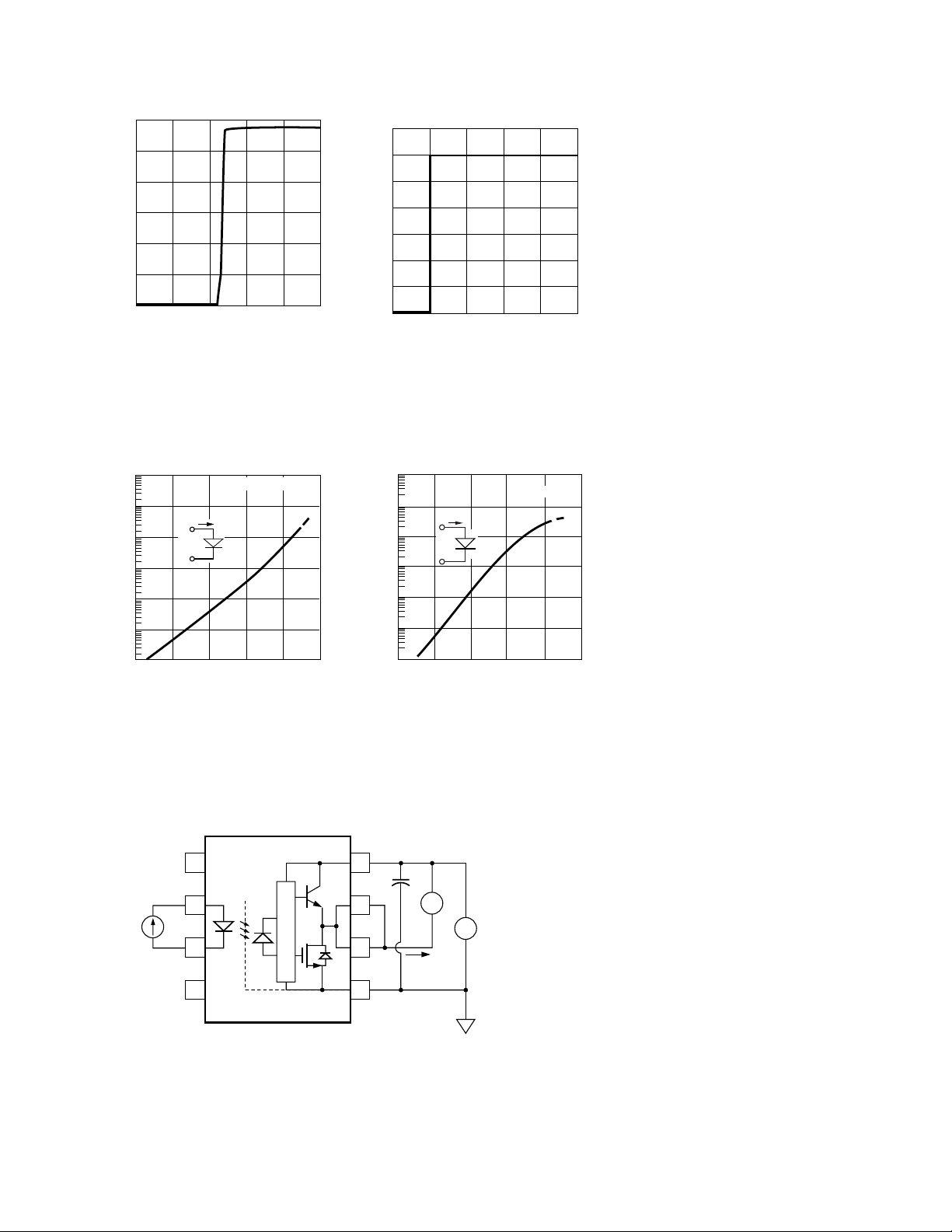
Figure 15. Transfer characteristics.
V
O
– OUTPUT VOLTAGE – V
0
0
IF – FORWARD LED CURRENT – mA
5
25
15
1
30
253 4
20
10
V
O
– OUTPUT VOLTAGE – V
0
0
IF – FORWARD LED CURRENT – mA
1352
5
5
15
25
3 4
10
20
HCPL-J312
30
I
F
– FORWARD CURRENT – mA
1.10
0.001
VF – FORWARD VOLTAGE – VOLTS
1.60
10
1.0
0.1
1.20
1000
1.30 1.40 1.50
TA = 25°C
I
F
V
F
+
–
0.01
100
HCPL-3120
VF – FORWARD VOLTAGE – VOLTS
1.2 1.3 1.4 1.5
I
F
– FORWARD CURRENT – mA
1.71.6
1.0
I
F
+
TA = 25°C
–
HCPL-J312/HCNW3120
V
F
0.1
0.01
0.001
10
100
1000
0.1 µF
V
CC
= 15
to 30 V
1
3
IF = 7 to
16 mA
+
–
2
4
8
6
7
5
+
–
4 V
I
OH
Figure 16. Input current vs. forward voltage.
Figure 17. IOH test circuit.
15
Page 16
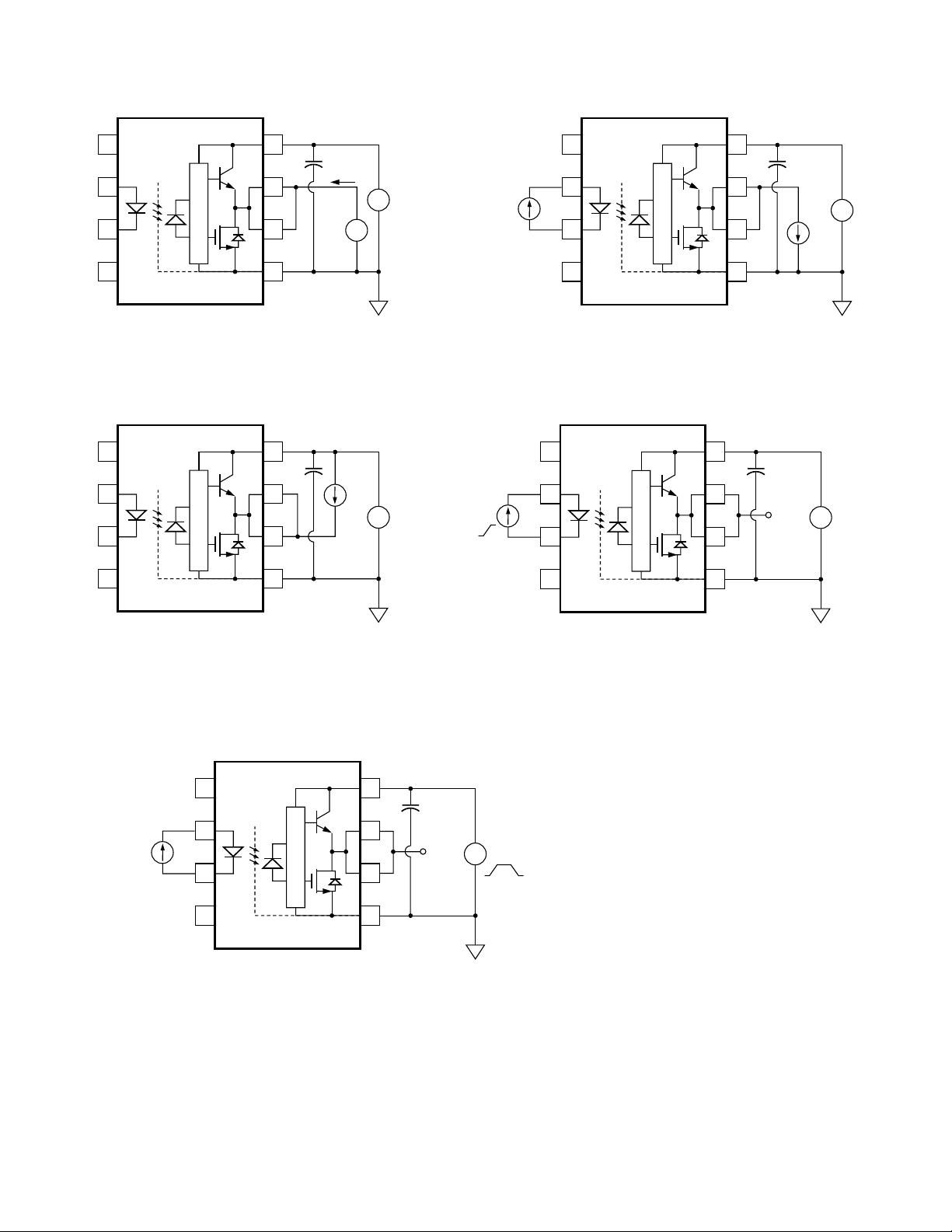
Figure 19. VOH Test circuit.Figure 18. IOL Test circuit.
0.1 µF
V
CC
= 15
to 30 V
1
3
+
–
2
4
8
6
7
5
2.5 V
I
OL
+
–
0.1 µF
V
CC
= 15
to 30 V
1
3
IF = 7 to
16 mA
+
–
2
4
8
6
7
5
100 mA
V
OH
0.1 µF
V
CC
= 15
to 30 V
1
3
+
–
2
4
8
6
7
5
100 mA
V
OL
0.1 µF
V
CC
= 15
to 30 V
1
3
I
F
+
–
2
4
8
6
7
5
VO > 5 V
0.1 µF
V
CC
1
3
IF = 10 mA
+
–
2
4
8
6
7
5
VO > 5 V
Figure 20. VOL Test circuit. Figure 21. I
Figure 22. UVLO test circuit.
16
Test circuit.
FLH
Page 17
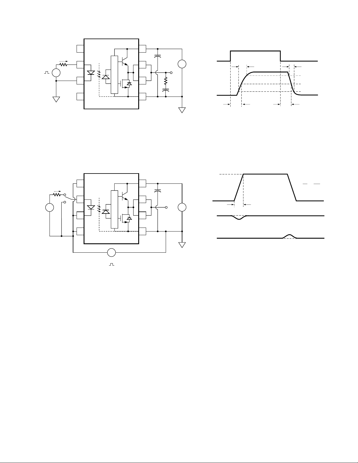
Figure 23. t
0.1 µF
V
CC
= 15
to 30 V
10 Ω
1
3
IF = 7 to 16 mA
V
O
+
–
+
–
2
4
8
6
7
5
10 KHz
50% DUTY
CYCLE
500 Ω
10 nF
I
F
V
OUT
t
PHL
t
PLH
t
f
t
r
10%
50%
90%
0.1 µF
V
CC
= 30 V
1
3
I
F
V
O
+
–
+
–
2
4
8
6
7
5
A
+
–
B
V
CM
= 1500 V
5 V
V
CM
∆t
0 V
V
O
SWITCH AT B: IF = 0 mA
V
O
SWITCH AT A: IF = 10 mA
V
OL
V
OH
∆t
V
CM
δV
δt
=
, t
, tr, and tf test circuit and waveforms.
PLH
PHL
Figure 24. CMR test circuit and waveforms.
17
Page 18
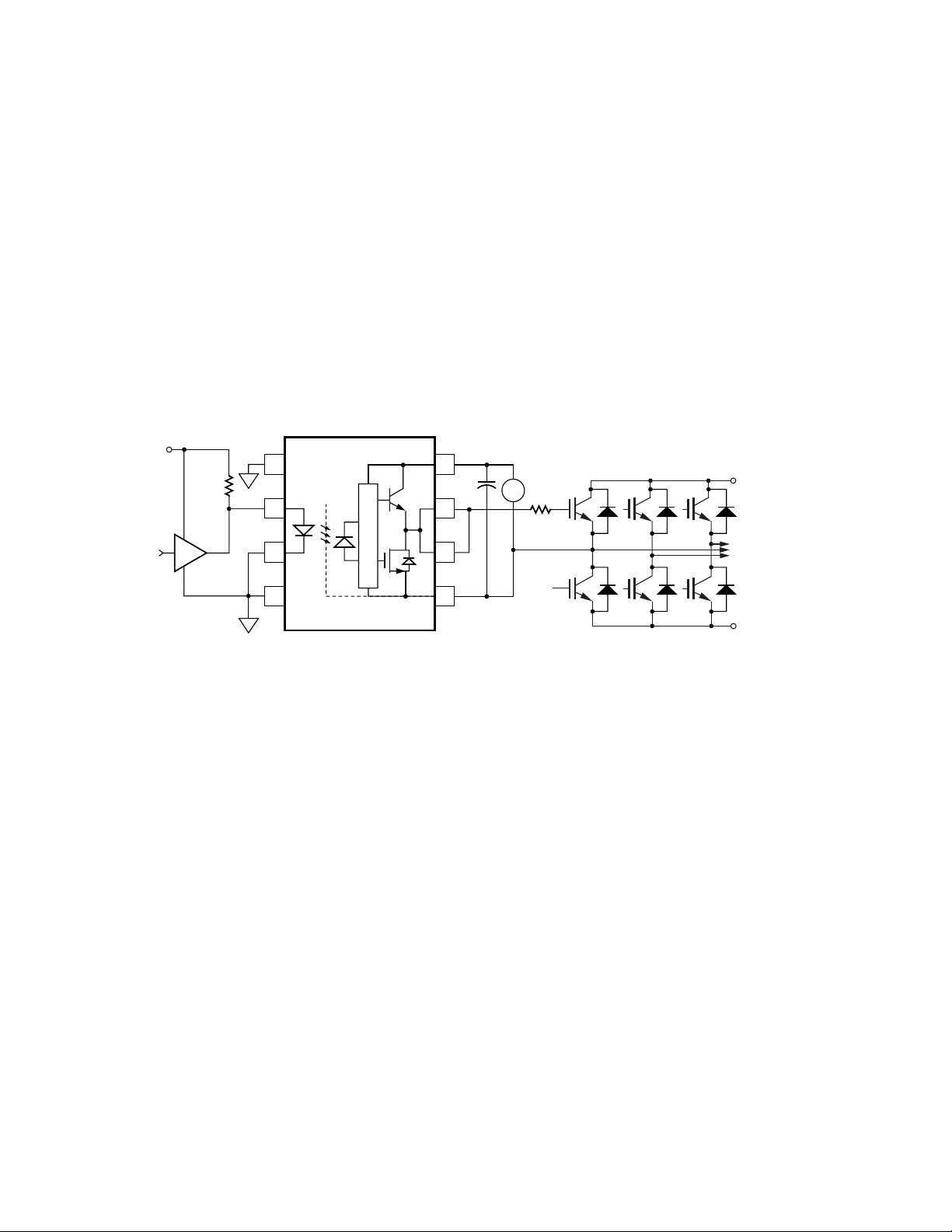
Applications Information
+ HVDC
3-PHASE
AC
- HVDC
0.1 µF
V
CC
= 18 V
1
3
+
–
2
4
8
6
7
5
270 Ω
HCPL-3120
+5 V
CONTROL
INPUT
Rg
Q1
Q2
74XXX
OPEN
COLLECTOR
Eliminating Negative IGBT Gate Drive (Discussion applies
to HCPL-3120, HCPL-J312, and HCNW3120)
To keep the IGBT rmly o, the HCPL-3120 has a very
low maximum VOL specication of 0.5 V. The HCPL-3120
realizes this very low VOL by using a DMOS transistor
with 1 Ω (typical) on resistance in its pull down circuit.
When the HCPL-3120 is in the low state, the IGBT gate
is shorted to the emitter by Rg + 1 Ω. Minimizing Rg
and the lead inductance from the HCPL-3120 to the
IGBT gate and emitter (possibly by mounting the HCPL-
3120 on a small PC board directly above the IGBT) can
eliminate the need for negative IGBT gate drive in many
applications as shown in Figure 25. Care should be taken
with such a PC board design to avoid routing the IGBT
collector or emitter traces close to the HCPL-3120 input
as this can result in unwanted coupling of transient
signals into the HCPL-3120 and degrade performance. (If
the IGBT drain must be routed near the HCPL-3120 input,
then the LED should be reverse-biased when in the o
state, to prevent the transient signals coupled from the
IGBT drain from turning on the HCPL-3120.)
Figure 25. Recommended LED drive and application circuit.
18
Page 19
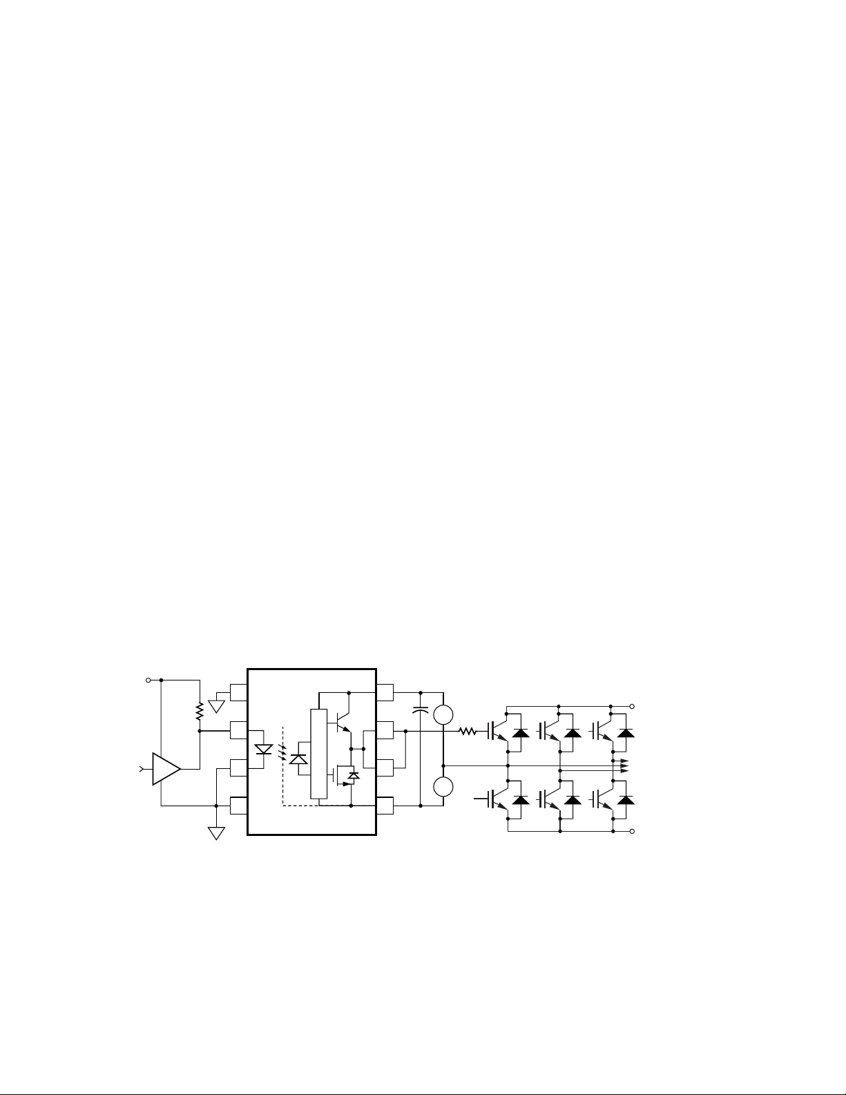
Selecting the Gate Resistor (Rg) to Minimize IGBT
+ HVDC
3-PHASE
AC
- HVDC
0.1 µF
V
CC
= 15 V
1
3
+
–
2
4
8
6
7
5
HCPL-3120
Rg
Q1
Q2
V
EE
= -5 V
–
+
270 Ω
+5 V
CONTROL
INPUT
74XXX
OPEN
COLLECTOR
Switching Losses. (Discussion applies to HCPL-3120,
HCPL-J312 and HCNW3120)
For the circuit in Figure 26 with IF (worst case) =
16 mA, Rg = 8 Ω, Max Duty Cycle = 80%, Qg = 500 nC,
f = 20 kHz and TA max = 85 °C:
Step 1: Calculate Rg Minimum from the IOL Peak Specication. The IGBT and Rg in Figure 26 can be analyzed as a
simple RC circuit with a voltage supplied by the HCPL-
3120.
(VCC – VEE - VOL)
Rg ≥ ———————
I
= ———————
I
(15 V + 5 V - 2 V)
= ———————
2.5 A
= 7.2 Ω @ 8 Ω
OLPEAK
(VCC – VEE - 2 V)
OLPEAK
The VOL value of 2 V in the previous equation is a conservative value of VOL at the peak current of 2.5A (see
Figure 6). At lower Rg values the voltage supplied by
the HCPL-3120 is not an ideal voltage step. This results
in lower peak currents (more margin) than predicted by
this analysis. When negative gate drive is not used VEE in
the previous equation is equal to zero volts.
Step 2: Check the HCPL-3120 Power Dissipation and
Increase Rg if Necessary. The HCPL-3120 total power
dissipation (PT) is equal to the sum of the emitter power
(PE) and the output power (PO):
PT = PE + P
O
PE = IF • VF · Duty Cycle
PO = P
O(BIAS)
+ P
O (SWITCHING)
= ICC • (VCC - VEE)+ ESW(RG, QG) • f
PE = 16 mA • 1.8 V • 0.8 = 23 mW
PO = 4.25 mA • 20 V + 5.2 µ J • 20 kHz
= 85 mW + 104 mW
= 189 mW > 178 mW (P
O(MAX)
@ 85°C
= 250 mW-15C*4.8 mW/C)
The value of 4.25 mA for ICC in the previous equation was
obtained by derating the ICC max of 5 mA (which occurs
at -40°C) to ICC max at 85C (see Figure 7).
Since PO for this case is greater than P
O(MAX)
, Rg must be
increased to reduce the HCPL-3120 power dissipation.
P
O(SWITCHING MAX)
= P
O(MAX)
- P
O(BIAS)
= 178 mW - 85 mW
= 93 mW
P
E
SW(MAX)
f
93 mW
= ———— = 4.65 µW
= ———————
O(SWITCHINGMAX)
20 kHz
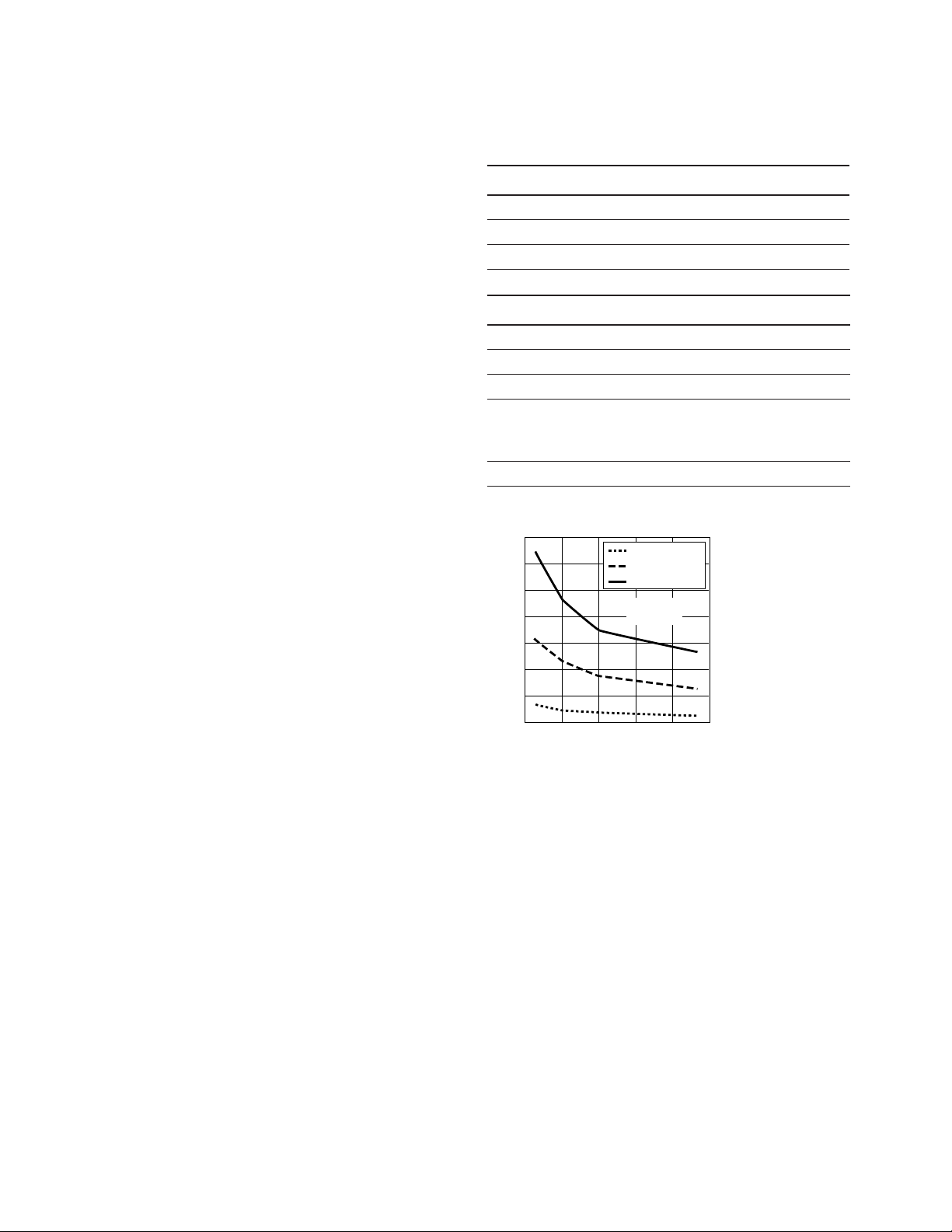
For Qg = 500 nC, from Figure 27, a value of ESW = 4.65 µW
gives a Rg = 10.3 Ω.
Figure 26. HCPL-3120 typical application circuit with negative IGBT gate drive.
19
Page 20
Esw – ENERGY PER SWITCHING CYCLE – µJ
0
0
Rg – GATE RESISTANCE – Ω
50
6
101420430 40
12
Qg = 100 nC
Qg = 500 nC
Qg = 1000 nC
10
8
2
VCC = 19 V
VEE = -9 V
Thermal Model (Discussion applies to HCPL-3120, HCPLJ312 and HCNW3120)
The steady state thermal model for the HCPL-3120 is
shown in Figure 28. The thermal resistance values given
in this model can be used to calculate the temperatures
at each node for a given operating condition. As shown
by the model, all heat generated ows through q
CA
which
raises the case temperature TC accordingly. The value
of qCA depends on the conditions of the board design
and is, therefore, determined by the designer. The value
of qCA = 83°C/W was obtained from thermal measurements using a 2.5 x 2.5 inch PC board, with small traces
(no ground plane), a single HCPL-3120 soldered into the
center of the board and still air. The absolute maximum
power dissipation derating specications assume a
qCAvalue of 83°C/W.
From the thermal mode in Figure 28 the LED and detector
IC junction temperatures can be expressed as:
TJE = P
qLC * q
+ PD•(——————— + qCA) + T
qLC + qDC + q
qLC • q
TJD = PE (——————— + qCA)
qLC + qDC + q
@
(qLC||(qLD + qDC) + qCA)
E
DC
LD
DC
LD
A
PE Parameter Description
IF LED Current
VF LED On Voltage
Duty Cycle Maximum LED Duty Cycle
PO Parameter Description
ICC Supply Current
VCC Positive Supply Voltage
VEE Negative Supply Voltage
ESW(Rg,Qg) Energy Dissipated in the HCPL-3120
for each IGBT Switching Cycle
(See Figure 27)
f Switching Frequency
+ PD • (qDC||(qLD + qLC) + qCA) + T
A
Inserting the values for qLC and qDC shown in Figure 28
gives:
TJE = PE • (256°C/W + qCA)
+ PD • (57°C/W + qCA) + T
TJD = PE • (57°C/W + qCA)
+ PD • (111°C/W + qCA) + T
A
Figure 27. Energy dissipated in the HCPL-3120 for each IGBT switching
A
cycle.
For example, given PE = 45 mW, PO = 250 mW, TA = 70°C
and qCA = 83°C/W:
TJE = P
• 339°C/W + PD • 140°C/W + TA
E
= 45 mW • 339°C/W + 250 mW
• 140°C/W + 70°C = 120°C
TJD = P
• 140°C/W + PD • 194°C/W + TA
E
= 45 mW • 140°C/W + 250 mW • 194°C/W + 70°C = 125°C
TJE and TJD should be limited to 125°C based on the
board layout and part placement (qCA) specic to the application.
20
Page 21
TJE = LED junction temperature
θLD = 442 °C/W
T
JE
T
JD
θLC = 467 °C/W θDC = 126 °C/W
θCA = 83 °C/W*
T
C
T
A
T
JE
= LED JUNCTION TEMPERATURE
T
JD
= DETECTOR IC JUNCTION TEMPERATURE
TC = CASE TEMPERATURE MEASURED AT THE
CENTER OF THE PACKAGE BOTTOM
θ
LC
= LED-TO-CASE THERMAL RESISTANCE
θ
LD
= LED-TO-DETECTOR THERMAL RESISTANCE
θ
DC
= DETECTOR-TO-CASE THERMAL RESISTANCE
θ
CA
= CASE-TO-AMBIENT THERMAL RESISTANCE
*
θ
CA
WILL DEPEND ON THE BOARD DESIGN AND
THE PLACEMENT OF THE PART.
1
3
2
4
8
6
7
5
C
LEDP
C
LEDN
1
3
2
4
8
6
7
5
C
LEDP
C
LEDN
SHIELD
C
LEDO1
C
LEDO2
TJD = detector IC junction temperature
TC = case temperature measured at the center of the package bottom
qLC = LED-to-case thermal resistance
qLD = LED-to-detector thermal resistance
qDC = detector-to-case thermal resistance
qCA = case-to-ambient thermal resistance
*qCA will depend on the board design and the placement of the part.
Figure 28. Thermal model.
LED Drive Circuit Considerations for Ultra High CMR Performance. (Discussion applies to HCPL-3120, HCPL-J312,
and HCNW3120)
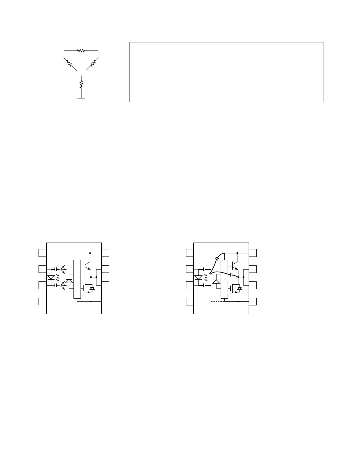
Without a detector shield, the dominant cause of optocoupler CMR failure is capacitive coupling from the
input side of the optocoupler, through the package, to
the detector IC as shown in Figure 29. The HCPL-3120
improves CMR perform-ance by using a detector IC with
an optically transparent Faraday shield, which diverts the
capacitively coupled current away from the sensitive IC
circuitry. However, this shield does not eliminate the capacitive coupling between the LED and optocoupler pins
5-8 as shown in Figure 30. This capacitive coupling causes
perturbations in the LED current during common mode
transients and becomes the major source of CMR failures
for a shielded optocoupler. The main design objective of
a high CMR LED drive circuit becomes keeping the LED
in the proper state (on or o) during common mode
transients. For example, the recommended application
circuit (Figure 25), can achieve 25 kV/µs CMR while minimizing component complexity.
Techniques to keep the LED in the proper state are
discussed in the next two sections.
Figure 29. Optocoupler input to output capacitance model for unshielded
optocouplers.
21
Figure 30. Optocoupler input to output capacitance model for shielded
optocouplers.
Page 22
CMR with the LED On (CMRH).
Rg
1
3
V
SAT
2
4
8
6
7
5
+
V
CM
I
LEDP
C
LEDP
C
LEDN
SHIELD
* THE ARROWS INDICATE THE DIRECTION
OF CURRENT FLOW DURING –dVCM/dt.
+5 V
+
–
V
CC
= 18 V
• • •
• • •
0.1
µF
+
–
–
1
3
2
4
8
6
7
5
C
LEDP
C
LEDN
SHIELD
+5 V
1
3
2
4
8
6
7
5
C
LEDP
C
LEDN
SHIELD
+5 V
Q1
I
LEDN
V
O
– OUTPUT VOLTAGE – V
0
0
(VCC - VEE ) – SUPPLY VOLTAGE – V
10
5
14
10 15
2
20
6
8
4
12
(12.3, 10.8)
(10.7, 9.2)
(10.7, 0.1)
(12.3, 0.1)
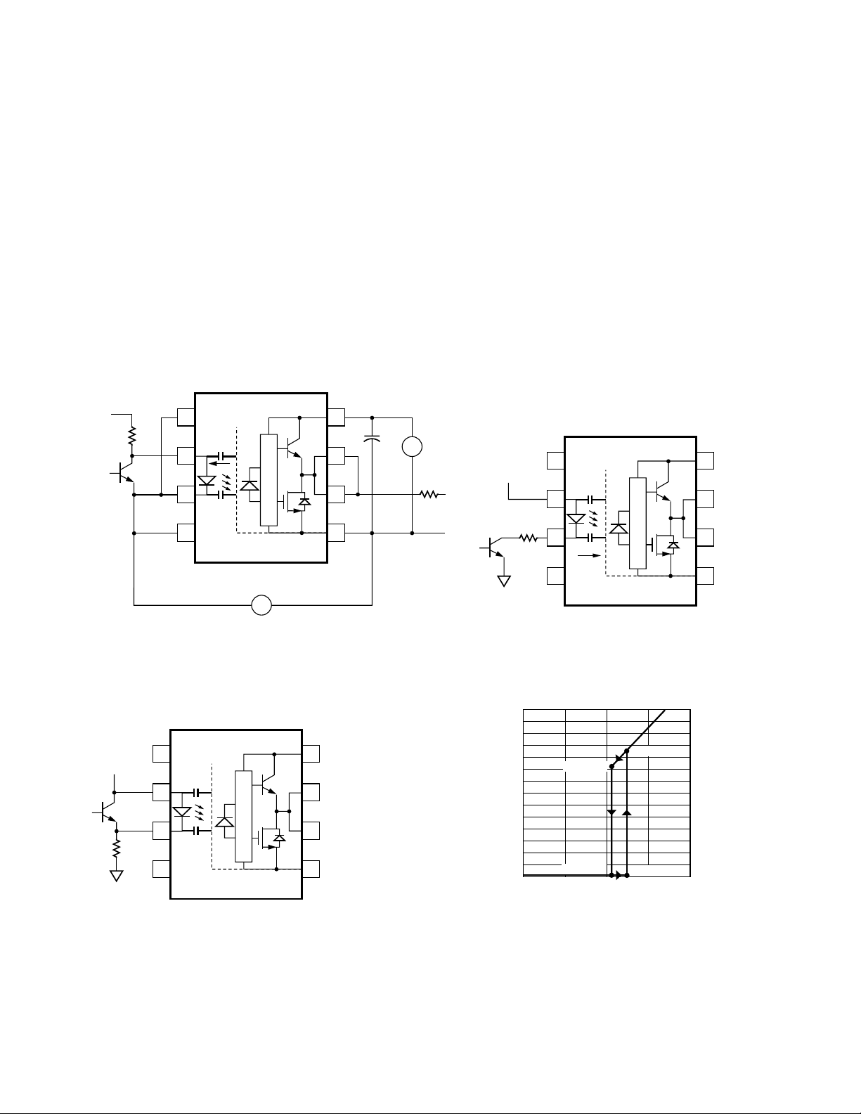
A high CMR LED drive circuit must keep the LED on during
common mode transients. This is achieved by overdriving the LED current beyond the input threshold so that
it is not pulled below the threshold during a transient.
A minimum LED current of 10 mA provides adequate
margin over the maximum I
of 5 mA to achieve 25 kV/
FLH
µs CMR.
CMR with the LED O (CMRL).
A high CMR LED drive circuit must keep the LED o
(VF ≤ V
example, during a -dVcm/dt transient in Figure 31, the
current owing through C
) during common mode transients. For
F(OFF)
also ows through the
LEDP
R
SAT
and V
of the logic gate. As long as the low state
SAT
voltage developed across the logic gate is less than
V
, the LED will remain o and no common mode
F(OFF)
failure will occur.
The open collector drive circuit, shown in Figure 32,
cannot keep the LED o during a +dVcm/dt transient,
since all the current owing through C
LEDN
must be
supplied by the LED, and it is not recommended for
applica-tions requiring ultra high CMRL performance.
Figure 33 is an alternative drive circuit which, like the recommended applica-tion circuit (Figure 25), does achieve
ultra high CMR performance by shunting the LED in the
o state.
Figure 31. Equivalent circuit for gure 25 during common mode transient. Figure 32. Not recommended open collector drive circuit.
Figure 33. Recommended LED drive circuit for ultra-high CMR.
22
Figure 34. Under voltage lock out.
Page 23
Under Voltage Lockout Feature. (Discussion applies to
t
PHL MAX
t
PLH MIN
PDD* MAX = (t
PHL- tPLH)MAX
= t
PHL MAX - tPLH MIN
*PDD = PROPAGATION DELAY DIFFERENCE
NOTE: FOR PDD CALCULATIONS THE PROPAGATION DELAYS
ARE TAKEN AT THE SAME TEMPERATURE AND TEST CONDITIONS.
V
OUT1
I
LED2
V
OUT2
I
LED1
Q1 ON
Q2 OFF
Q1 OFF
Q2 ON
t
PLH
MIN
MAXIMUM DEAD TIME
(DUE TO OPTOCOUPLER)
= (t
PHL MAX - tPHL MIN
) + (t
PLH MAX - tPLH MIN
)
= (t
PHL MAX - tPLH MIN
) – (t
PHL MIN - tPLH MAX
)
= PDD* MAX – PDD* MIN
*PDD = PROPAGATION DELAY DIFFERENCE
NOTE: FOR DEAD TIME AND PDD CALCULATIONS ALL PROPAGATION
DELAYS ARE TAKEN AT THE SAME TEMPERATURE AND TEST CONDITIONS.
V
OUT1
I
LED2
V
OUT2
I
LED1
Q1 ON
Q2 OFF
Q1 OFF
Q2 ON
t
PHL MIN
t
PHL MAX
t
PLH MAX
PDD* MAX
(t
PHL-tPLH) MAX
HCPL-3120, HCPL-J312, and HCNW3120)
The HCPL-3120 contains an under voltage lockout (UVLO)
feature that is designed to protect the IGBT under fault
conditions which cause the HCPL-3120 supply voltage
(equivalent to the fully-charged IGBT gate voltage) to
drop below a level necessary to keep the IGBT in a low resistance state. When the HCPL-3120 output is in the high
state and the supply voltage drops below the HCPL3120 V
coupler output will go into the low state with a typical
delay, UVLO Turn O Delay, of 0.6 µs.
When the HCPL-3120 output is in the low state and
the supply voltage rises above the HCPL-3120 V
threshold (11.0 < V
will go into the high state (assumes LED is “ON”) with a
typical delay, UVLO Turn On Delay of 0.8 µs.
threshold (9.5 < V
UVLO–
UVLO+
< 12.0) the opto-
UVLO–
UVLO+
< 13.5) the optocoupler output
IPM Dead Time and Propagation Delay Specications.
(Discussion applies to HCPL-3120, HCPL-J312, and
HCNW3120)
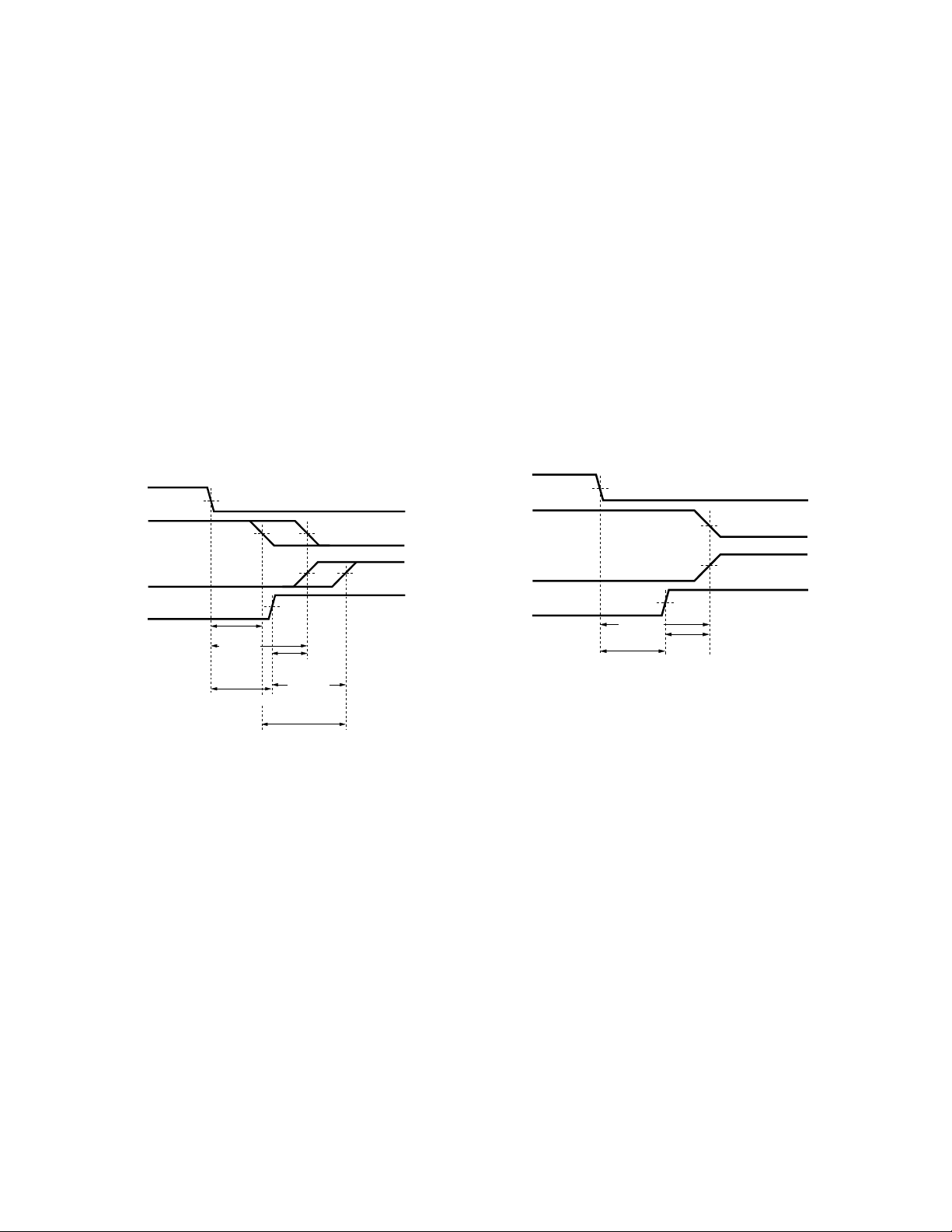
The HCPL-3120 includes a Propagation Delay Dierence
(PDD) specication intended to help designers minimize
“dead time” in their power inverter designs. Dead time
is the time period during which both the high and low
side power transistors (Q1 and Q2 in Figure 25) are o.
Any overlap in Q1 and Q2 conduction will result in large
currents owing through the power devices between
the high and low voltage motor rails.
Figure 36. Waveforms for dead time.
23
Figure 35. Minimum LED skew for zero dead time.
Page 24
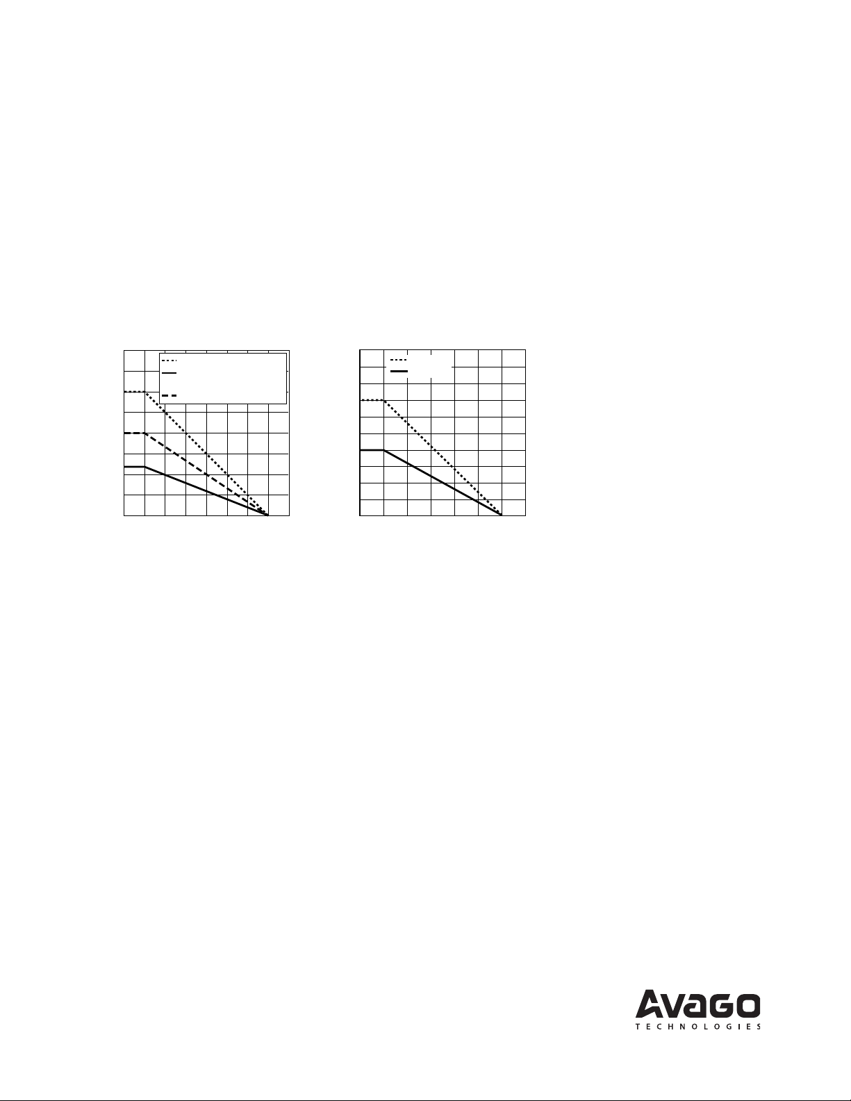
OUTPUT POWER – P
S
, INPUT CURRENT – I
S
0
0
TS – CASE TEMPERATURE – °C
175
1000
50
400
12525 75 100 150
600
800
200
100
300
500
700
900
HCNW3120
PS (mW)
IS (mA)
OUTPUT POWER – P
S
, INPUT CURRENT – I
S
0
0
TS – CASE TEMPERATURE – °C
200
600
400
25
800
50 75 100
200
150 175
PS (mW)
125
100
300
500
700
IS (mA) FOR HCPL-3120
OPTION 060
IS (mA) FOR HCPL-J312
HCPL-3120 OPTION 060éHCPL-J312
To minimize dead time in a given design, the turn on of
LED2 should be delayed (relative to the turn o of LED1)
so that under worst-case con-ditions, transistor Q1 has
just turned o when transistor Q2 turns on, as shown in
Figure 35. The amount of delay necessary to achieve this
conditions is equal to the maximum value of the propagation delay dierence specication, PDD
, which is
MAX
specied to be 350 ns over the operating temperature
range of -40°C to 100°C.
Delaying the LED signal by the maximum propagation
delay dierence ensures that the minimum dead time is
zero, but it does not tell a designer what the maximum
dead time will be. The maximum dead time is equivalent
to the dierence between the maximum and minimum
propagation delay dierence specications as shown in
Figure 36. The maximum dead time for the HCPL-3120 is
700 ns (= 350 ns - (-350 ns)) over an operating temperature range of -40°C to 100°C.
Note that the propagation delays used to calculate PDD
and dead time are taken at equal temperatures and test
conditions since the optocouplers under consideration
are typically mounted in close proximity to each other
and are switching identical IGBTs.
Figure 37. Thermal derating curve, dependence of safety limiting value with case temperature per IEC/EN/DIN EN 60747-5-2.
For product information and a complete list of distributors, please go to our website: www.avagotech.com
Avago, Avago Technologies, and the A logo are trademarks of Avago Technologies in the United States and other countries.
Data subject to change. Copyright © 2005-2008 Avago Technologies. All rights reserved. Obsoletes AV01-0622EN
AV02-0161EN - July 4, 2008
 Loading...