

Page 1
BCD-TO-7 SEGMENT LATCH/DECODER/LCD DRIVER
DISPLAY BLANKING OF ALL ILLEGAL INPUT
COMBINATIONS
LATCH STORAGE OF CODE
CAPABILITY OF DRIVING TWO LOW POWER
TTL LOADS,TWO HTLLOADS, OR ONE LOW
POWER SCHOTTKY LOAD OVER THE FULL
RATED-TEMPERATURE RANGE
PIN-FOR-PIN REPLACEMENT FOR THE
HCF4056B(with pin 7 tiedto VSS)
DIRECTLED DRIVING CAPABILITY
100% TESTED FOR QUIESCENT CURRENT
AT 20V
MAXIMUM INPUT CURRENT OF 1A AT 18V
OVER FULL PACKAGE-TEMPERATURE
RANGE ; 100nAAT 18V AND 25°C
NOISEMARGIN (full package-temperature
range) = 1V AT VDD=5V
2V AT VDD= 10V
2.5VAT VDD= 15V
5-V, 10-V, AND 15-V PARAMETRIC RATINGS
Appl icati ons :
INSTRUMENT DISPLAY DRIVER
DASHBOARD DISPLAYDRIVER
COMPUTER/CALCULATORDISPLAYDRIVER
TIMING DEVICE DRIVER (clocks, watches,
timers)
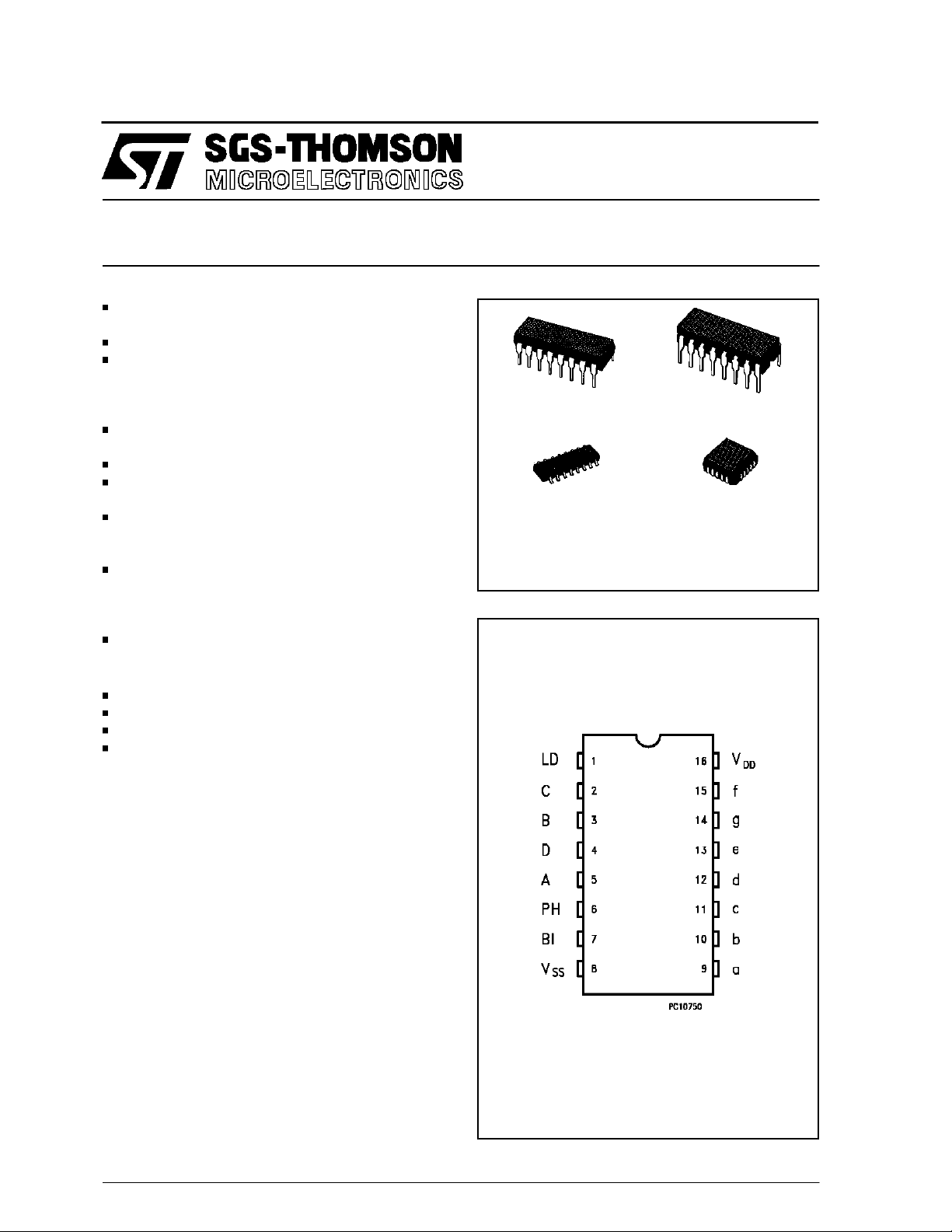
HCC/HCF4543B
HCC4 54 3B
HCF4543B
EY
(Plastic Package)
M1
(Micro Package)
ORDER CODES :
HCC 4543 BF HCF4543 B M1
HCF4543 BEY HCF4543 B C 1
PIN CONNEC TION (top vie w)
(Ceramic FritSeal Package)
(Plastic Chip Carrier)
F
C1
DESCRI PTION
The HCC/HCF4543B is a BCD-to-seven segment
latch/decoder/driver designed primarily for liquidcrystaldisplay(LCD) applications. It isalso capable
of driving light emitting diode (LED), incandescent,
gas-discharge, and fluorescent displays. This deviceis functionally similar to andservesas direct replacement for the HCF4056B when pin 7 is
connected to VSS. It differsfrom the HCF4056B in
that it has a displayblanking capability instead of a
level-shifting function and requires only one power
supply. When the HCF4056B is used in the level
shifting mode, two power supplies are required.
When the HCF4543B isused for LCD applications,
a squarewave mustbe applied to thePHASEinput
and the backplane of the LCD device.For LED applications a logic 1 is required at the PHASE input
for common-cathode devices ; a logic 0 is required
for common-anode devices (see truthtable).
December1989
1/12
Page 2
HCC/HCF4543B
ABSOLU TE MAXIMU M RAT INGS
Symbol Parameter Value Unit
V
* Supply voltage: HCC Types
DD
HCF Types
Input Voltage – 0.5 to VDD+ 0.5 V
V
i
DC Input Current (any one input) ± 10 mA
I
I
Total Power Dissipation (per package)
P
tot
Dissipation per OutputTransistor
= Full Package-temperature Range
for T
op
Operating Temperature : HCC Types
T
op
HCF Types
Storage Temperature – 65to + 150 °C
T
stg
* All Voltage Values are referred to VSSpin voltage.
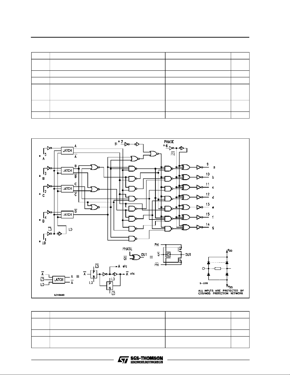
LOGI C DIAG RAM (1/2 of d ev i ce show n)
– 0.5 to + 20
– 0.5 to 18
200
100
– 55to + 125
–40to+85
mW
mW
°C
°C
V
V
RECOMMENDED OPERATING CONDITIONS
Symbol Parameter Value Unit
V
2/12
Supply Voltage: HCC Types
DD
HCF Types
V
Input Voltage 0 to V
I
T
Operating Temperature : HCC Types
op
HCF Types
3to+18
3to+15
DD
– 55to + 125
–40to+85
°C
°C
V
V
V
Page 3
HCC/HCF4543B
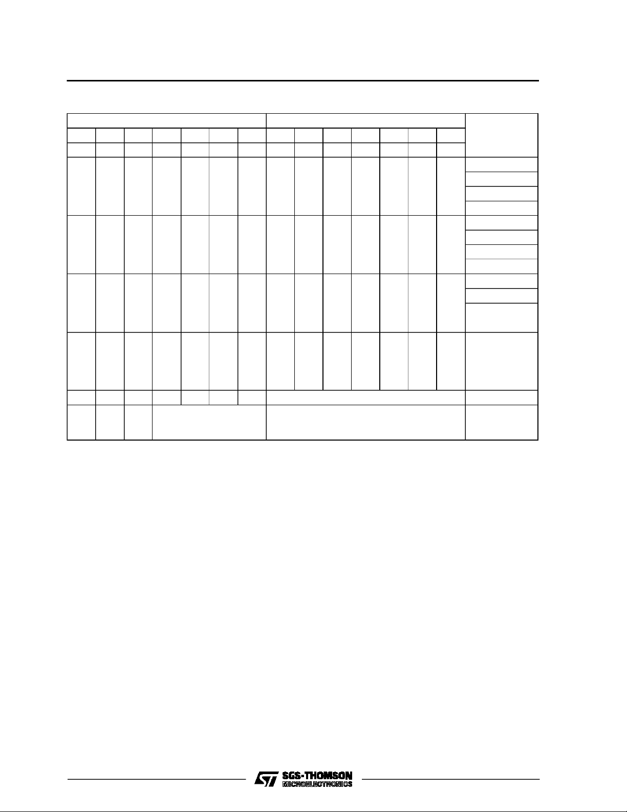
TRUTH TABLE
INPUT CODE OUTPUT S TATE
LDBIPh*DCBAabcd e f g
X10XXXX0000000
10000001111110 0
10000010110000 1
10000101101101 2
10000111111001 3
10001000110011 4
10001011011011 5
10001101011111 6
10001111110000 7
10010001111111 8
10010011111011 9
10010100000000 Blank
10010110000000 Blank
10011000000000 Blank
10011010000000 Blank
10011100000000 Blank
10011110000000 Blank
000XXXX ** **
Inverseof Output
••• •
Combinations
Above
X = Don’t care.
• = Above combinations
* = For liquid-crystal readouts, apply a square wave to Ph.
For common cathode LED readouts, select Ph = 0.
For common anode LED readouts, select Ph = 1.
** = Depends upon the BCD code previously applied when LD = 1.
DIS PLAY
CHARACTER
Display
as above
3/12
Page 4
HCC/HCF4543B
STATI C ELECT RIC AL CHAR ACTER I STI CS
Test Con ditions Value
Symbol Parameter
I
Quiescent
L
Current
HCC
Types
V
(V)
V
I
(V)
I
O
(µA)
V
(V)
DD
O
0/5 5 5 0.04 5 150
0/10 10 10 0.04 10 300
0/15 15 20 0.04 20 600
T
Low
Min. Max. Min. Typ. Max. Min. Max.
0/20 20 100 0.08 100 3000
0/5 5 5 0.04 5 150
HCF
Types
0/10 10 10 0.04 10 300
0/15 15 20 0.04 20 600
V
OH
OutputHigh
Voltage
0/5 < 1 5 4.95 4.95 4.95
0/10 < 1 10 9.95 9.95 9.95
0/15 < 1 15 14.95 14.95 14.95
V
OL
OutputLow
Voltage
5/0 < 1 5 0.05 0.05 0.05
10/0 < 1 10 0.05 0.05 0.05
15/0 < 1 15 0.05 0.05 0.05
V
IH
InputHigh
Voltage
0.5/4.5 < 1 5 3.5 3.5 3.5
1/9 < 1 10 7 7 7
1.5/13.5 < 1 15 11 11 11
V
IL
InputLow
Voltage
4.5/0.5 < 1 5 1.5 1.5 1.5
9/1 < 1 10 3 3 3
13.5/1.5 < 1 15 4 4 4
Output
I
OH
Drive
Current
HCC
Types
0/5 2.5 5 – 1.6 – 1.3 – 2.6 – 0.9
0/5 4.6 5 – 0.46 – 0.37 – 0.75 – 0.26
0/10 9.5 10 – 0.98 – 0.8 – 1.6 – 0.55
0/15 13.5 15 – 3.33 – 2.7 – 5.4 – 1.9
0/5 2.5 5 1.3 – 1.1 – 2.6 – 0.9
HCF
0/5 4.6 5 0.36 – 0.31 – 0.75 – 0.25
Types
0/10 9.5 10 0.81 – 0.68 – 1.6 – 0.54
0/15 13.5 15 2.7 – 2.3 – 5.4 – 1.84
Output
I
OL
Sink
Current
HCC
Types
0/5 0.4 5 0.64 0.51 1 0.36
0/10 0.5 10 1.6 1.3 2.6 0.9
0/15 1.5 15 4.2 3.4 6.8 2.4
0/5 0.4 5 0.52 0.44 1 0.36
HCF
Types
0/10 0.5 10 1.3 1.1 2.6 0.9
0/15 1.5 15 3.6 3.0 6.8 2.4
Input
I
IH,IIL
Leakage
Current
*T
=–55°C for HCC device : – 40°C for HCF device.
Low
*T
= + 125°C for HCC device : + 85°C for HCF device.
High
The Noise Margin for both ”1” and ”0” level is : 1V min. with VDD= 5V, 2V min. with VDD= 10V, 2.5V min. with VDD= 15V.
HCC
0/18
types
HCF
0/15 15 ± 0.3 ± 10
types
Any Input
18 ± 0.1 ±10
25°CT
–5
± 0.1 ± 1
-5
± 0.3 ± 1
High
Unit
µA
V
V
V
V
mA
mA
µA
4/12
Page 5

HCC/HCF4543B
DYNAMICELECTRICAL CHARACTERISTICS (T
=25°C, CL= 50pF, RL=200kΩ,
amb
typicaltemperature coefficient for all VDDvalues is 0.3%/°C, all input riseand falltime = 20ns)
Limits
All p ackages
600
200
150
500
200
150
180
90
65
180
90
65
250
100
80
60
20
10
125
50
40
15
–5
–5
25
20
10
20
1200
400
300
1000
400
300
360
180
130
360
180
130
-5
0
Symbo l Pa rameter
t
Propagation Delay Time 5
PHL
t
PLH
Transition Time 5
t
THL
t
TLH
LatchDisable Pulse Width 5
t
WH
t
Address Setup Time 5
SU
t
Address Hold Time 5
H
C
Input Capacitance Any Input 5 7.5 pF
IN
Test Co ndition s
(V)
V
DD
10
15
5
10
15
10
15
5
10
15
10
15
10
15
10
15
Min. Typ. Max.
Unit
ns
BCD-to-seven-segment latch/decoder/driver functional diagram
5/12
Page 6

HCC/HCF4543B
TypicalOutput Low (sink)Current Characteristics. Minimum OutputLow(sink)Current Characteristics.
Typical Transition Time as a Function of Load Capacitance
TypicalDinamicPower Dissipation asa Functionof
Frequency
Typical Propagation Delay Time as a Function of
Load Capacitance
6/12
Page 7

HCC/HCF4543B
Input Voltage Test Circuit. Quiescent Device CurrentTest Circuit.
Input-leakage -current Test Circuit.
7/12
Page 8

HCC/HCF4543B
Plastic DIP16 (0.25) MECHANICAL DATA
DIM.
MIN. TYP. MAX. MIN. TYP. MAX.
a1 0.51 0.020
B 0.77 1.65 0.030 0.065
b 0.5 0.020
b1 0.25 0.010
D 20 0.787
E 8.5 0.335
e 2.54 0.100
e3 17.78 0.700
F 7.1 0.280
I 5.1 0.201
L 3.3 0.130
Z 1.27 0.050
mm inch
8/12
P001C
Page 9

Ceramic DIP16/1 MECHANICAL DATA
HCC/HCF4543B
DIM.
MIN. TYP. MAX. MIN. TYP. MAX.
A 20 0.787
B 7 0.276
D 3.3 0.130
E 0.38 0.015
e3 17.78 0.700
F 2.29 2.79 0.090 0.110
G 0.4 0.55 0.016 0.022
H 1.17 1.52 0.046 0.060
L 0.22 0.31 0.009 0.012
M 0.51 1.27 0.020 0.050
N 10.3 0.406
P 7.8 8.05 0.307 0.317
Q 5.08 0.200
mm inch
P053D
9/12
Page 10

HCC/HCF4543B
SO16 (Narrow) MECHANICAL DATA
DIM.
MIN. TYP. MAX. MIN. TYP. MAX.
A 1.75 0.068
a1 0.1 0.2 0.004 0.007
a2 1.65 0.064
b 0.35 0.46 0.013 0.018
b1 0.19 0.25 0.007 0.010
C 0.5 0.019
c1 45° (typ.)
D 9.8 10 0.385 0.393
E 5.8 6.2 0.228 0.244
e 1.27 0.050
e3 8.89 0.350
F 3.8 4.0 0.149 0.157
G 4.6 5.3 0.181 0.208
L 0.5 1.27 0.019 0.050
M 0.62 0.024
S8°(max.)
mm inch
10/12
P013H
Page 11

PLCC20 MECHANICAL DATA
HCC/HCF4543B
DIM.
MIN. TYP. MAX. MIN. TYP. MAX.
A 9.78 10.03 0.385 0.395
B 8.89 9.04 0.350 0.356
D 4.2 4.57 0.165 0.180
d1 2.54 0.100
d2 0.56 0.022
E 7.37 8.38 0.290 0.330
e 1.27 0.050
e3 5.08 0.200
F 0.38 0.015
G 0.101 0.004
M 1.27 0.050
M1 1.14 0.045
mm inch
P027A
11/12
Page 12

HCC/HCF4543B
Information furnished is believed to be accurate and reliable. However, SGS-THOMSON Microelectronics assumes no responsability for the
consequences of use of such information nor for any infringement of patents or other rights of third parties which may results from its use. No
license is grantedby implication or otherwise underany patentor patent rights of SGS-THOMSON Microelectronics. Specificationsmentioned
in this publication are subject to change without notice. This publication supersedes and replaces all information previously supplied.
SGS-THOMSON Microelectronicsproductsare notauthorized foruse ascritical componentsin life support devices orsystems withoutexpress
written approval of SGS-THOMSON Microelectonics.
1994 SGS-THOMSON Microelectronics - All Rights Reserved
Australia - Brazil - France - Germany - Hong Kong - Italy - Japan - Korea - Malaysia - Malta - Morocco - The Netherlands -
Singapore - Spain - Sweden - Switzerland - Taiwan - Thailand - UnitedKingdom - U.S.A
SGS-THOMSON Microelectronics GROUP OF COMPANIES
12/12
 Loading...