

Page 1
.CASCADABLE IN MULTIPLES OF 4-BITS
.SET TO9 INPUTAND 9 DETECT OUTPUT
.QUIESCENT CURRENT SPECIFIED TO 20V
FOR HCC DEVICE
.STANDARDIZED SYMMETRICAL OUTPUT
CHARACTERISTICS
.5V, 10VAND 15V PARAMETRIC RATINGS
.INPUT CURRENTOF 100nA AT 18V AND25
FOR HCC DEVICE
o
.100% TESTEDFOR QUIESCENTCURRENT
.MEETSALLREQUIREMENTSOFJEDECTEN-
TATIVE STANDARD N. 13A, ” STANDARD
SPECIFICATIONS FOR DESCRIPTION OF B
SERIESCMOS DEVICES ”
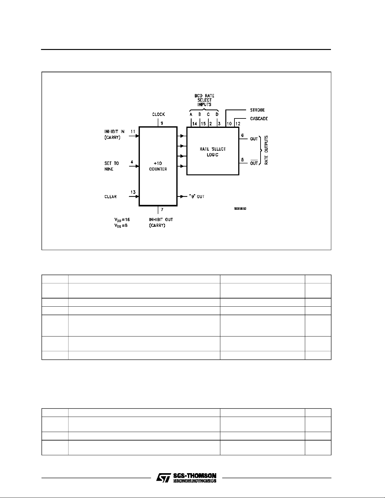
HCC4527B
HCF4527B
BCD RATE MULTIPLEXER
C
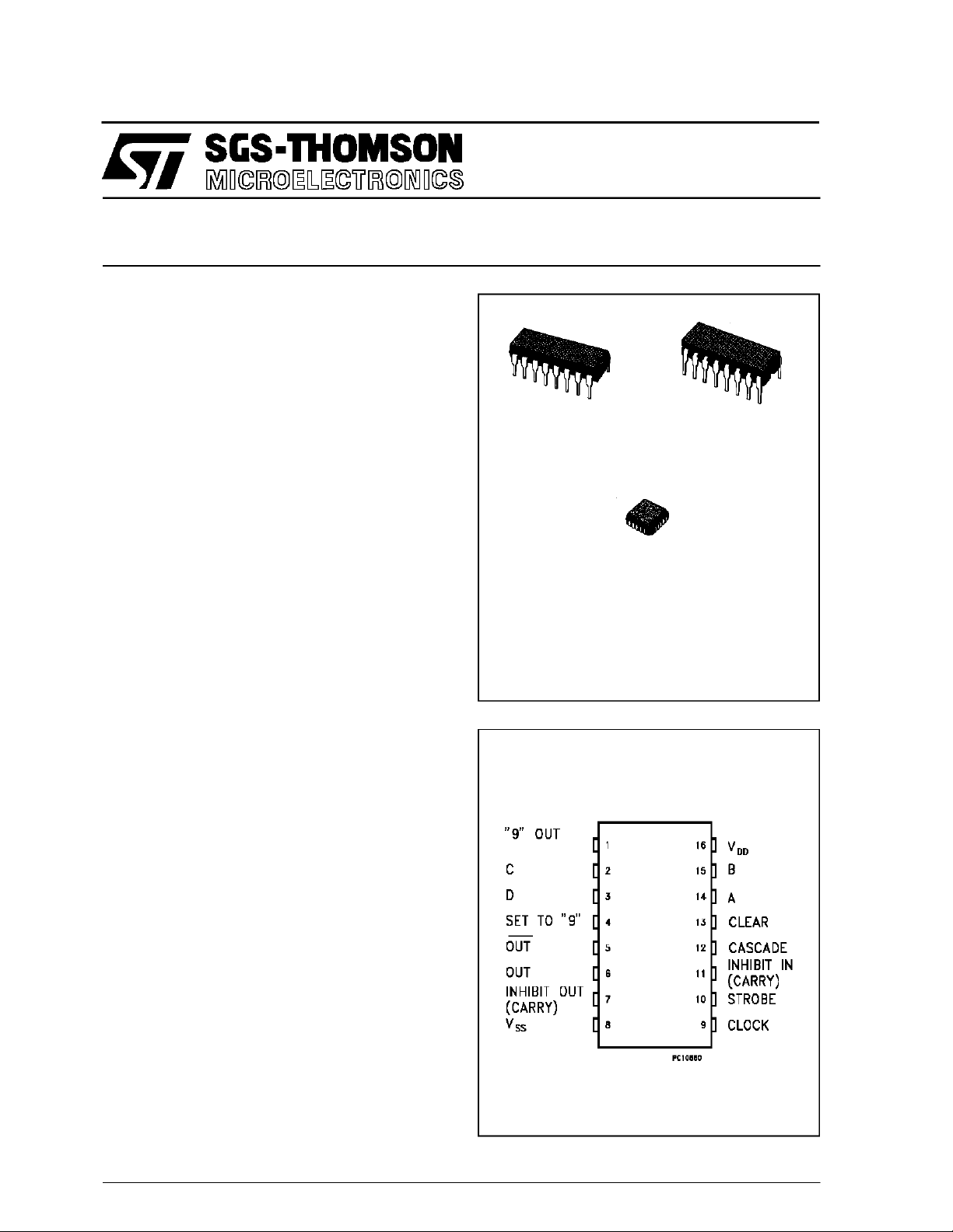
EY
(PlasticPackage)
F
(CeramicPackage)
C1
(ChipCarrier)
DESCRIPTION
TheHCC4527B (extended temperature range) and
HCF4527B (intermediate temperature range) are
monolithic integrated circuit, available in 16-lead
dual in line plastic or ceramicpackage.
TheHCC/HCF4527Bisalow power4bitdigital rate
multiplier thatprovidesan output pulserate whichis
theclockinputpulseratemultipliedby1/10timesthe
BCD input. For example, when the BCDinput is 8,
there will be 8 output pulses for every 10 input
pulses. This device may be used to preform arithmetic operations (add, subtract, divide, raise to a
power), solve algebraic and differential equations,
generate naturel logarithms and trigonometric func-
ORDER CODES :
HCC4 076BF HCF4076BEY
HCF4076BC1
PIN CONNECTIONS
September 1990
1/13
Page 2
HCC/HCF4527B
FUN CTIONAL DIAGR A M
ABSOLU TE M AXIMU M R AT ING
Symbol Parameter Value Unit
* Supply Voltage: HCC Types
V
DD
HCF Types
V
P
Input Voltage -0.5 to VDD+ 0.5 V
i
I
DC Input Current (any oneinput) ± 10 mA
I
Total Power Dissipation (per package)
tot
-0.5 to +20
-0.5 to +18
200
V
V
mW
Dissipation per Output Transistor
for Top = Full Package Temperature Range
T
Operating Temperature: HCC Types
op
HCF Types
T
Stressesabove thoselistedunder ”Absolute MaximumRatings”maycausepermanent damagetothedevice. Thisisastressratingonlyand functional
operation of the device atthese oranyother conditions above thoseindicated in theoperational sections of thisspecification is not implied.Exposure
to absolute maximum ratingconditions forexternal periodsmay affectdevice reliability.
* All voltagevalues are referred to VSSpinvoltage.
Storage Temperature -65 to +150
stg
100
-55 to +125
-40 to +85
mW
o
C
o
C
o
C
RECO MM ENDED OPERATIN G CO NDI TIONS
Symbol Parameter Value Unit
V
Supply Voltage: HCC Types
DD
HCF Types
V
T
Input Voltage 0 to V
I
Operating Temperature: HCC Types
op
HCF Types
3to18
3to15
DD
-55 to +125
-40 to +85
V
V
V
o
C
o
C
2/13
Page 3

LOGI C DI AGRAM
HCC/HCF4527B
3/13
Page 4

HCC/HCF4527B
TRUTH TABLE
Inputs Outputs
Number of Pulsed or Logic Level
(0 = Low; 1 = High; X = Don’t Care)
DCBA CLKINHINSTR CAS CLR SET OUT OUT
0000 10 00000LH11
0001 10 000001111
0010 10 000002211
0011 10 000003311
0100 10 000004411
0101 10 000005511
0110 10 000006611
0111 10 000007711
1000 10 000008811
1001 10 000009911
1010 10 000008811
1011 10 000009911
1100 10 000008811
1101 10 000009911
1110 10 000008811
1111 10 000009911
XXXX 10 10000■■H■
XXXX 10 01000LH11
XXXX 10 00100H●11
1XXX10000101010HL
0XXX1000010LHHL
XXXX 10 00001LHLH
●Output same asthe first16 linesofthistruthtable(depending on valueofA, B, C, D)
■ Depends on internal stateof counter.
Number of Pulses or Output
Logic Level
(L = LOW; H = High)
INH
OUT
”9”
OUT
4/13
Page 5

HCC/HCF4527B
STATI C ELE CT RIC AL CHA R ACTE R ISTI CS (over recomm ended operatin g conditio ns)
Test Conditios Value
Symbol Parameter
Quiescent
I
L
Current
HCC
Types
V
(V)
V
I
(V)
|IO|
(µA)
V
(V)
O
T
DD
*25
LOW
Min. Max. Min. Typ. Max. Min. Max.
0/5 5 5 0.04 5 150
0/10 10 10 0.04 10 300
0/15 15 20 0.04 20 600
o
CT
0/20 20 100 0.08 100 3000
HCF
Types
0/5 5 20 0.04 20 150
0/10 10 40 0.04 40 300
0/15 15 80 0.04 80 600
OH
Output High
V
Voltage
0/5 < 1 5 4.95 4.95 4.95
0/10 < 1 10 9.95 9.95 9.95
0/15 < 1 15 14.95 14.95 14.95
OL
Output Low
V
Voltage
5/0 < 1 5 0.05 0.05 0.05
10/0 < 1 10 0.05 0.05 0.05
15/0 < 1 15 0.05 0.05 0.05
IH
Input High
V
Voltage
0.5/4.5 < 1 5 3.5 3.5 3.5
1/9 < 1 10 7 7 7
1.5/13.5 < 1 15 11 11 11
IL
Input Low
V
Voltage
4.5/0.5 < 1 5 1.5 1.5 1.5
9/1 < 1 10 3 3 3
13.5/1.5 < 1 15 4 4 4
OH
Output
Drive
Current
HCC
Types
I
0/5 2.5 5 -2 -1.6 -3.2 -1.15
0/5 4.6 5 -0.64 -0.51 -1 -0.36
0/10 9.5 10 -1.6 -1.3 -2.6 -0.9
0/15 13.5 15 -4.2 -3.4 -6.8 -2.4
0/5 2.5 5 -1.53 -1.36 -3.2 -1.1
HCF
Types
0/5 4.6 5 -0.52 -0.44 -1 -0.36
0/10 9.5 10 -1.3 -1.1 -2.6 -0.9
0/15 13.5 15 -3.6 -3.0 -6.8 -2.4
I
OL
Output
Sink
Current
HCC
Types
HCF
Types
0/5 0.4 5 0.64 0.51 1 0.36
0/10 0.5 10 1.6 1.3 2.6 0.9
0/15 1.5 15 4.2 3.4 6.8 2.4
0/5 0.4 5 0.53 0.44 1 0.36
0/10 0.5 10 1.3 1.1 2.6 0.9
0/15 1.5 15 3.6 3.0 6.8 2.4
I
IH,IIL
Input Leakage
Current
C
*T
LOW
*T
HIGH
TheNoiseMarginfor both ”1” and”0”level is: 1V min. withVDD=5V,2 V min.withVDD=10V,2.5 V min. withVDD=15V
Input Capacitance Any Input 5 7.5 pF
I
=-55oCforHCC device: -40oC for HCF device.
=+125oCfor HCCdevice:+85oC for HCFdevice.
0/18
0/15 15 ±0.3 ±10
Any Input
18 ±0.1 ±10-5±0.1 ±1 µA
-5
±0.3 ±1 µA
HIGH
Unit
*
µA
V
V
V
V
mA
mA
5/13
Page 6

HCC/HCF4527B
DYNAMIC ELECTRICAL CHARACTERISTICS (T
=25oC, CL=50pF,RL= 200 KΩ,
amb
typic al temperature coeff ic ent for all VDDvalues is 03 %/oC, all input ri s e and fall ti mes = 20 ns)
Symbol Parameter
t
t
t
t
t
PLH
PHL
PLH
PHL
PLH
Propagation Delay Time
Clock to Output)
Propagation Delay Time
Clock or Strobe to Output
Propagation Delay Time
Clock to Inhibit Output
t
PHL
Propagation Delay Time
Clock to Inhibit Output
t
PLH
t
PHL
t
PLH
t
PHL
t
PLH
t
PHL
t
PLH
t
PHL
t
PLH
t
PHL
t
THL
t
TLH
f
t
t
r,tf
t
t
setup
Propagation Delay Time
Clear to Output
Propagation Delay Time
Clock to ”9” or ”1” Q Output
Propagation Delay Time
Cascade to Output
Propagation Delay Time
Inhibit Input to Inhibit Output
Propagation Delay Time
Set to Output
Transition Time 5 100 200
Maximum Clock Frequency 5 1.2 2.4
CL
Clock Pulse Width 5 330 165
W
Clock Rise or Fall Time 5 15
Set or Clear Pulse Width 5 160 80
W
Inhibit Input Setup Time 5 100 50
Test Conditions Value
(V) Min. Typ. Max.
V
DD
5 110 220
10 55 110
15 45 90
5 150 300
10 75 150
15 60 120
5 320 640
10 145 290
15 100 200
5 250 500
10 100 200
15 75 150
5 380 760
10 175 550
15 130 260
5 300 600
10 125 250
15 90 180
5 90 180
10 45 90
15 35 70
5 130 260
10 60 120
15 45 90
5 330 660
10 150 300
15 110 220
10 50 100
15 40 80
10 2.5 5
15 3.5 7
10 170 85
15 100 50
10 15
15 15
10 90 45
15 60 30
10 40 20
15 20 10
Unit
ns
ns
ns
ns
ns
ns
ns
ns
ns
ns
MHz
ns
µs
ns
ns
6/13
Page 7

DYNAMIC ELECTRICAL CHARACTERISTICS (continued)
HCC/HCF4527B
Symbol Parameter
t
Inhibit Input Removal Time 5 240 120
R
Set Remova Time 5 150 75
t
R
t
Clear RemovalTime 5 60 30
R
APPLICATION NOTE
For fractional multipliers with more than one digit,
HCC/HCF4527B devices may be cascated in two
differentmodes: theAddmode andtheMltiplymode
(see figures1 and2).
When two units are cascated in Addmode and programmedto 9and 4 respectively, the more significantunit will have9 outputpulses for every10 input
pulses and the other unit willhave 4 output pulses
for every 100 input pulses for a totalof:
9
4
10
+
100
=
94
100
Test Conditions Value
(V) Min. Typ. Max.
V
DD
10 130 65
15 110 55
10 80 40
15 50 25
10 40 20
15 30 15
Unit
ns
ns
ns
In the multiply mode, the fraction programmed into
the first rate multiplier is multiplied by the fraction
programmed into the secondone:
If N1= 9 and N2=4
out
out
out
4
=
2
1
2
f
out
1
10
9
=
f
clock
10
4
=
10
9
×
10
f
clock
36
=
f
100
clock
f
f
f
Therefore 36outputpulsesfor every100 clockinput
pulses.
7/13
Page 8

HCC/HCF4527B
Fig. 1: Two HCC/HCF4527B Cascaded in The ”Add” Mode With a Preset Number
Fig. 2: Two HCC/HCF4527B Cascaded in The ”Multiply” Mode With a Preset Number
8/13
Page 9

Fig. 3: Timing Diagram (see Logic Diagram)
HCC/HCF4527B
9/13
Page 10

HCC/HCF4527B
Plastic DIP16 (0.25) MECHANICAL DATA
DIM.
MIN. TYP. MAX. MIN. TYP. MAX.
a1 0.51 0.020
B 0.77 1.65 0.030 0.065
b 0.5 0.020
b1 0.25 0.010
D 20 0.787
E 8.5 0.335
e 2.54 0.100
e3 17.78 0.700
F 7.1 0.280
I 5.1 0.201
L 3.3 0.130
Z 1.27 0.050
mm inch
10/13
P001C
Page 11

Ceramic DIP16/1 MECHANICAL DATA
HCC/HCF4527B
DIM.
MIN. TYP. MAX. MIN. TYP. MAX.
A 20 0.787
B 7 0.276
D 3.3 0.130
E 0.38 0.015
e3 17.78 0.700
F 2.29 2.79 0.090 0.110
G 0.4 0.55 0.016 0.022
H 1.17 1.52 0.046 0.060
L 0.22 0.31 0.009 0.012
M 0.51 1.27 0.020 0.050
N 10.3 0.406
P 7.8 8.05 0.307 0.317
Q 5.08 0.200
mm inch
P053D
11/13
Page 12

HCC/HCF4527B
PLCC20 MECHANICAL DATA
DIM.
MIN. TYP. MAX. MIN. TYP. MAX.
A 9.78 10.03 0.385 0.395
B 8.89 9.04 0.350 0.356
D 4.2 4.57 0.165 0.180
d1 2.54 0.100
d2 0.56 0.022
E 7.37 8.38 0.290 0.330
e 1.27 0.050
e3 5.08 0.200
F 0.38 0.015
G 0.101 0.004
M 1.27 0.050
M1 1.14 0.045
mm inch
12/13
P027A
Page 13

HCC/HCF4527B
Information furnished is believed to be accurate and reliable. However, SGS-THOMSON Microelectronics assumes no responsability forthe
consequences of use of such information nor for any infringement of patents or other rights of third parties which may results from its use. No
license is granted byimplicationor otherwise under any patentor patent rights ofSGS-THOMSON Microelectronics. Specificationsmentioned
in this publication aresubject to changewithout notice.This publication supersedes andreplaces all information previously supplied.
SGS-THOMSON Microelectronicsproducts are not authorized foruse ascritical componentsinlife supportdevices orsystems without express
written approval of SGS-THOMSON Microelectonics.
1994 SGS-THOMSON Microelectronics- All RightsReserved
Australia - Brazil - France - Germany - Hong Kong - Italy - Japan - Korea - Malaysia - Malta - Morocco - The Netherlands-
Singapore -Spain - Sweden - Switzerland - Taiwan - Thailand - UnitedKingdom - U.S.A
SGS-THOMSON Microelectronics GROUP OF COMPANIES
13/13
 Loading...