

Page 1

24 STAGE FREQUENCY DIVIDER
■ VERYLOW QUIESCENT CURRENT
■
HIGHNOISEIMMUNITY
■ VOLTAGESUPPLYRANGE3V TO18V
■
ALLSTAGESARERESETTABLE
■ RESETDISABLESTHE RC OSCILLATORFOR
LOWSTANDBYPOWERDRAIN
■
RC AND CRYSTALOSCILLATOROUTPUT
ARECAPABLEOF DRIVING EXTERNAL
LOADS
DESCRIPTION
The HCF4521B is a monolithic integrated circuit,
available in 16-lead dual-in-line plastic package
and plasticmicro packages.
The HCF4521B have a chain of 24 flip-flops with
an input circuit that allows three modes of
operation. The input circuit functions as a crystal
or an RC oscillator or as an input buffer for an
external oscillator. Each flip-flop performs a
divide-by-twofunction giving a total count of 2
16,777,216.The count advances on the negative
goingedge of the clock.Access is available to the
final seven stages giving the device added
flexibility.
24
HCF4521B
EY
(PlasticPackage)
ORDERCODES :
HCF4521BEY HCF4521BM1
=
M1
(Micro Package)
PIN CONNECTION
February 1999
1/12
Page 2
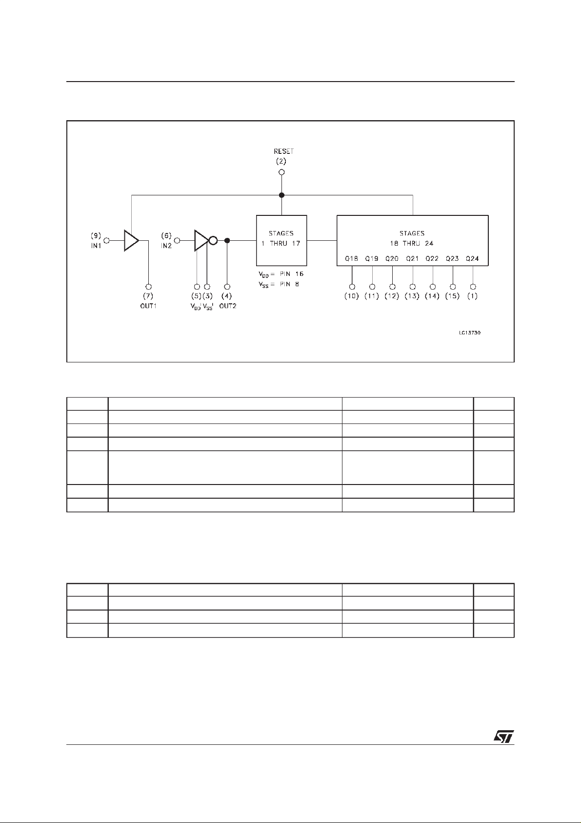
HCF4521
BLOCKDIAGRAM
ABSOLUTE MAXIMUM RATING
Symb o l Parameter Val u e Uni t
* Supply Voltage -0.5to+18 V
V
DD
Input Voltage -0.5toVDD+0.5 V
V
i
DC Input Current (any one input) ±10 mA
I
I
Total Power Dissipation (per package)
P
tot
200
mW
Dissipation per Output Transistor
for Top = Full Package Temperature Range
T
Operating Temperature -40to+85
op
Storage Temperature -65to+150
T
stg
Stressesabove those listed under ”Absolute Maximum Ratings” may cause permanent damage to the device. This is a stress rating only and functional
operation ofthedevice at these or any other conditions above thoseindicated in the operational sectionsof this specification is not implied. Exposure to
abso lute maximumratingconditions forexternalperiodsmayaffe c tdevicereliability.
*Allvoltage values arereferredtoV
pinvoltage.
SS
100
mW
o
C
o
C
RECOMMENDED OPERATINGCONDITIONS
Symb o l Parameter Val u e Uni t
V
Supply Voltage 3to15 V
DD
Input Voltage 0toV
V
I
Operating Temperature -40to+85
T
op
DD
V
o
C
2/12
Page 3

FUNCTIONALDIAGRAM
HCF4521
3/12
Page 4

HCF4521
STATICELECTRICAL CHARACTERISTICS
Referencesto V
Symb o l Parameter Test Conditi o s V a lue Uni t
I
Quiescent Current 0/5 5 20 0.04 20 150
L
SS
)
V
V
I
(V)
0/10 10 40 0.04 40 300
O
(V)
(over recommendedoperatingconditions, voltages
|I
O
(µA)
|
V
DD
(V)
o
C25
-40
Mi n . Max. Mi n . Typ. Max. M in. Max.
o
C85
o
C
µA
0/15 15 80 0.04 80 600
V
OH
Output High
Voltage
0/5 < 1 5 4.95 4.95 4.95
0/10 <1 10 9.95 9.95 9.95
0/15 <1 15 14.95 14.95 14.95
V
OL
Output Low
Voltage
5/0 < 1 5 0.05 0.05 0.05
10/0 <1 10 0.05 0.05 0.05
15/0 <1 15 0.05 0.05 0.05
V
IH
Input High
Voltage
0.5/4.5 < 1 5 3.5 3.5 3.5
1/9 <1 10 7 7 7
1.5/13.5 <1 15 11 11 11
V
IL
Input Low
Voltage
4.5/0.5 < 1 5 1.5 1.5 1.5
9/1 <1 10 3 3 3
13.5/1.5 <1 15 4 4 4
I
OH
Output Drive
Current
0/5 2.5 5 -1.53 -1.36 -3.2 -1.1
0/5 4.6 5 -0.52 -0.44 -1 -0.36
mA
0/10 9.5 10 -1.3 -1.1 -2.6 -0.9
0/15 13.5 15 -3.5 -3.0 -6.8 -2.4
I
Output Sink Current 0/5 0.4 5 0.52 0.44 1 0.36
OL
0/10 0.5 10 1.3 1.1 2.6 0.9
mA
0/15 1.5 15 3.6 3.0 6.8 2.4
I
TheNoiseMargin forboth ”1”and”0”level is:1Vmin.withVDD=5V,2 V min.withVDD=10V, 2.5V min.withVDD=15V
Input Leakage
IH,IIL
Current
C
Input Capacitance AnyInput 5 7.5
I
0/18 AnyInput 18
0.1
±
-5
0.1
10
±
±
1
±
µ
pF
V
V
V
V
A
4/12
Page 5

HCF4521
DYNAMICELECTRICALCHARACTERISTICS
typical temperaturecoefficentfor allV
valuesis 03%/oC, all inputrise andfalltimes=20 ns)
DD
=25oC, CL=50pF,RL= 200KΩ,
(T
amb
Symb o l Paramet er Test Conditi o ns V alu e Uni t
V
Min. Typ. Max.
DD
(V)
t
Output Rise Time 5 100 200
PLH
10 50 100
ns
15 40 80
t
Output Fall Time 5 100 200
PHL
10 50 100
ns
15 40 80
t
Propagation Delay Time Clock to Q18 5 4.5 9.0
PHL
t
PLH
10 1.7 3.5
µs
15 1.3 2.7
t
Propagation Delay Time Clock to Q24 5 6.0 12
PHL
t
PLH
10 2.2 4.5
µ
15 1.7 3.5
t
Propagation Delay Time RESET to Qn 5 1300 2600
PHL
10 500 1000
ns
15 375 750
t
Clock Pulse Width 5 385 140
WH(cl)
10 150 55
ns
15 120 40
f
Clock Pulse Frequency 5 3.5 2
cl
10 9 5
MHz
15 12 6.5
t
Clock Rise and Fall Time 5 15
TLH
t
THL
10 15
µ
15 15
t
Reset Pulse Width 5 1400 700
W(R)
10 600 300
ns
15 450 225
s
s
5/12
Page 6

HCF4521
TypicalOutput Low (sink) Current Characteristics Minimum OutputLow (sink)Current
Characteristics
TypicalOutput High (source)Current
Characteristics
TypicalPower Dissipationvs, Frequency
MinimumOutput High (source) Current
Characteristics
6/12
Page 7

HCF4521
FUNCTIONALTEST SEQUENCE
Inpu ts Outputs Comments
RESET I n2 O ut 2 V
100V
011V
000V
011V
011V
000V
000GNDGND 1
010GNDV
010GNDV
001GNDV
Atest function (see fig.8)has been included forthe reduction of test time required to exercise all 24 counter stages. Thistest function divides the counter
intothree8-stage sections and255counts areloadedineachofthe8-stage sectionsinparallel.Allflip-floparenowata logic”1”.Thecounter is now
returned tothenormal 24-stages inseries configuration. Onemorepulse isenteredintoInput 2 (In2)whichwillcause thecounterto ripplefroman all”1”
state to anall ”0”state.
’VDD’Q18thru
SS
Q24
GND 0 Counter is in three 8-stage sections in parallel mode.
DD
Counter is reset. In2 and Out2 are connected togheter
GND 0 First ”0” to ”1” transition on In2, Out2 node.
DD
GND 0 255 ”0” to ”1” transitions are clocked into this In2, Out2
DD
GND 0
DD
GND 1 The 255th ”0” to ”1” transition.
DD
GND 1
DD
DD
DD
DD
1 Counter converted back to 24-stages in series mode.
1 Out2 converts back toan output
0 Counter ripples from an all ”1” state to an all ”0” stage.
node.
RC OscillatorCircuit FunctionalTest Circuit
1
f≅
RTCC
2.3
2R
R
≥
S
TC
finHz,RinOhms,C inFarads
7/12
Page 8

HCF4521
TYPICALDATA FOR CRYSTAL OSCILLATORCIRCUIT
Characteristic 500 kHz
Crystal Characteristics
Resonant Frequency
Equivalent Reistance, R
S
External Resistor/Capacitor Values
R
O
C
T
C
S
Frequency Stability
Frequency Change as a Function of V
Change from 5V to 10V
V
DD
Change from 10V to 15V
V
DD
DD(TA
Frequency Change as a Function of Temperature (V
Change from -55oCto25oC
T
A
HCF4521B only
Complete Oscillator *
Change from 25oCto125oC
T
A
HCF4521B only
Complete Oscillator *
* Comple teoscillato rincludes crystal, capacitors and resistors.
CrystalOscillatorCircuit
=25oC)
=10V)
DD
CIRCUIT
500
1
47
82
20
6
2
-4
100
-2
-160
50 kHz CIRCUI T Unit
50
6.2
750
82
20
2
2
-2
120
-2
-560
kHz
k
Ω
kΩ
pF
pF
ppm
ppm
ppm
ppm
ppm
ppm
* Optional forlow power operation.
8/12
Page 9

TESTCIRCUITS
QuiescentDevice Current. Noise Immunity.
InputLeakage Current.
HCF4521
9/12
Page 10

HCF4521
Plastic DIP-16 (0.25) MECHANICAL DATA
DIM.
MIN. TYP. MAX. MIN. TYP. MAX.
a1 0.51 0.020
B 0.77 1.65 0.030 0.065
b 0.5 0.020
b1 0.25 0.010
D 20 0.787
E 8.5 0.335
e 2.54 0.100
e3 17.78 0.700
F 7.1 0.280
I 5.1 0.201
L 3.3 0.130
Z 1.27 0.050
mm inch
10/12
P001C
Page 11

SO-16 MECHANICAL DATA
HCF4521
DIM.
MIN. TYP. MAX. MIN. TYP. MAX.
A 1.75 0.068
a1 0.1 0.2 0.004 0.007
a2 1.65 0.064
b 0.35 0.46 0.013 0.018
b1 0.19 0.25 0.007 0.010
C 0.5 0.019
c1 45 (typ.)
D 9.8 10 0.385 0.393
E 5.8 6.2 0.228 0.244
e 1.27 0.050
e3 8.89 0.350
F 3.8 4.0 0.149 0.157
G 4.6 5.3 0.181 0.208
L 0.5 1.27 0.019 0.050
M 0.62 0.024
S 8 (max.)
mm inch
P013H
11/12
Page 12

HCF4521
Information furnished is believed to be accurate and reliable. However, STMicroelectronics assumes no responsibility for the consequences
of use of such information nor for any infringement of patents or other rights of third parties which may result from its use. No license is
granted by implication or otherwise under any patent or patent rights of STMicroelectronics. Specification mentioned in this publication are
subject tochange without notice. This publication supersedes and replaces all information previously supplied. STMicroelectronics products
are notauthorized for use as critical components inlife support devices or systems without express written approval of STMicroelectronics.
The ST logo is a trademarkof STMicroelectronics
1999 STMicroelectronics – Printed in Italy –All Rights Reserved
STMicroelectronics GROUP OF COMPANIES
Australia - Brazil - Canada - China - France -Germany - Italy - Japan - Korea - Malaysia - Malta - Mexico - Morocco - The Netherlands -
Singapore -Spain -Sweden - Switzerland - Taiwan - Thailand - United Kingdom - U.S.A.
http://www.st.com
.
12/12
 Loading...