

Page 1
HCF4086B
EXPANDABLE 4-WIDE 2-INPUT AND-OR INVERTER GATE
■ MEDIUM-SPEED OPERATION
t
= 90ns, t
PHL
■ INHIBIT AND ENABLE IN PUTS
■ QUIESCENT CURRENT SPECIFIED UP TO
= 140ns (Typ.) at 10V
PLH
20V
■ STANDARDIZED SYMMETRICAL OUTPUT
CHARACTERISTICS
■ 5V, 10V AND 15V PARAMETRIC RAT INGS
■ INPUT LEAKAGE CURRENT
I
= 100nA (MAX) AT VDD = 18V TA = 25°C
I
■ 100% TESTED FOR QUIESCENT CURRENT
■ MEETS ALL REQUIREMENTS OF JEDEC
JESD13B "STANDARD SPECIFICATIONS
FOR DESCRIPTI ON OF B SERI ES CMOS
DEVICES"
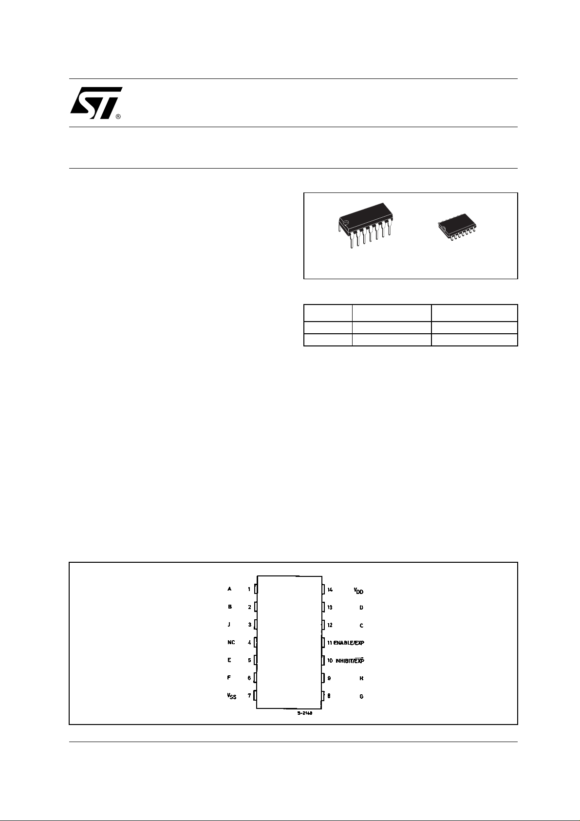
DESCRIPTION
HCF4086B is a monolithic integrated circuit
fabricated in Metal Oxide Semiconductor
technology available in DIP and SOP packages.
DIP SOP
ORDER CODES
PACKAGE TUBE T & R
DIP HCF4086BEY
SOP HCF4086BM1 HCF4086M013TR
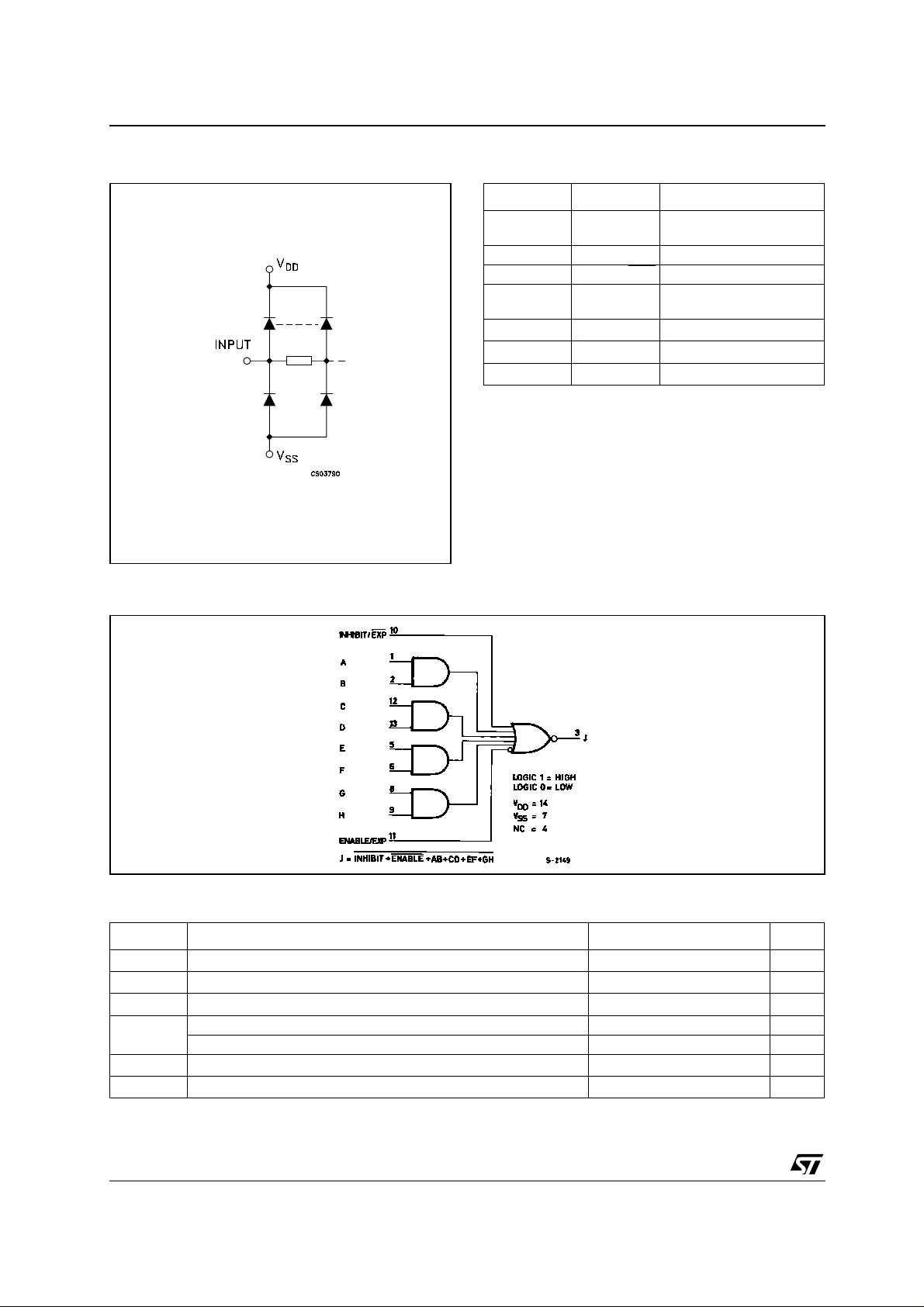
HCF4086B contains one 4 -wide 2-input AND-OR
INVERT gates with an INHIBIT EXP inp ut and an
ENABLE/EXP input. INHIBIT/EXP is tied to V
SS
and ENABLE/EXP to VDD. For a 4 wide A-O-I
function.
PIN CONNECTION
1/8September 2002
Page 2
HCF4086B
INPUT EQUIVALENT CIRCUIT PIN DESCRIPTION
PIN No SYMBOL NAME AND FUNCTION
1, 2, 12, 13,
5, 6, 8, 9
3 J Output
10 INHIBIT/EXP
10
4
7
14
A to H Data Inputs
ENABLE/
EXP
NC
V
SS
V
DD
Inhibit Input
Enable Input
Not Connected
Negative Supply Voltage
Positive Supply Voltage
FUNCTIONAL DIAGRAM
ABSOLUTE MAXIMUM RATINGS
Symbol Parameter Value Unit
V
V
P
T
T
Absolute Maximum Ratings are those values beyond which damage to the device may occur. Functional operation under these conditions is
not implied.
All voltage value s are referred to V
Supply Voltage
DD
DC Input Voltage -0.5 to VDD + 0.5
I
I
DC Input Current
I
Power Dissipation per Package 200 mW
D
-0.5 to +22 V
10 mA
±
Power Dissipation per Output Transistor 100 mW
Operating Temperature
op
Storage Temperature
stg
pin voltage.
SS
-55 to +125 °C
-65 to +150 °C
V
2/8
Page 3
HCF4086B
RECOMMENDED OPERATING CONDITIONS
Symbol Parameter Value Unit
V
V
T
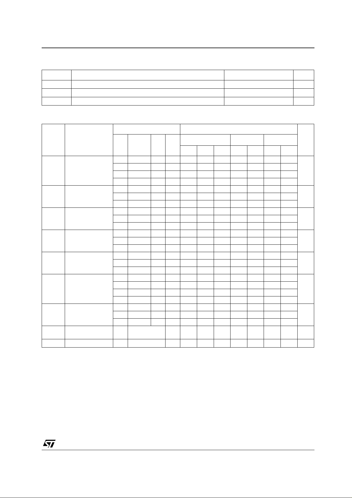
DC SPECIFICATIONS
Symbol Parameter
I
L
V
OH
V
OL
V
IH
V
IL
I
OH
I
OL
I
I
C
I
The Noi se Margin for both "1" a nd "0" level is: 1V min. wit h VDD=5V, 2V min. with VDD=10V, 2.5V min. with VDD=15V
Supply Voltage
DD
Input Voltage 0 to V
I
Operating Temperature
op
3 to 20 V
DD
-55 to 125 °C
Test Condition Value
V
(V)
= 25°C
V
I
(V)
|I
|
O
O
(µA)
V
DD
(V)
A
Min. Typ. Max. Min. Max. Min. Max.
-40 to 85°C -55 to 125°C
T
Quiescent Current 0/5 5 0.02 1 30 30
0/10 10 0.02 2 60 60
0/15 15 0.02 4 120 120
0/20 20 0.04 20 600 600
High Level Output
0/5 <1 5 4.95 4.95 4.95
Voltage
0/15 <1 15 14.95 14.95 14.95
Low Level Output
5/0 <1 5 0.05 0.05 0.05
Voltage
15/0 <1 15 0.05 0.05 0.05
High Level Input
0.5/4.5 <1 5 3.5 3.5 3.5
Voltage
1.5/13.5 <1 15 11 11 11
Low Level Input
4.5/0.5 <1 5 1.5 1.5 1.5
Voltage
13.5/1.5 <1 15 4 4 4
Output Drive
Current
0/5 2.5 <1 5 -1.36 -3.2 -1.15 -1.1
0/5 4.6 <1 5 -0.44 -1 -0.36 -0.36
0/10 9.5 <1 10 -1.1 -2.6 -0.9 -0.9
0/15 13.5 <1 15 -3.0 -6.8 -2.4 -2.4
Output Sink
0/5 0.4 <1 5 0.44 1 0.36 0.36
Current
0/15 1.5 <1 15 3.0 6.8 2.4 2.4
Input Leakage
Current
Input Capacitance
0/18 Any Input 18
Any Input 5 7.5 pF
-5
0.1
±
10
±
1
±
1
±
V
Unit
A
µ
V0/10 <1 10 9.95 9.95 9.95
V10/0 <1 10 0.05 0.05 0.05
V1/9 <1 10 7 7 7
V9/1 <1 10 3 3 3
mA
mA0/10 0.5 <1 10 1.1 2.6 0.9 0.9
A
µ
3/8
Page 4

HCF4086B
DYNAMIC ELECTRICAL CHARACTERISTICS (T
= 25°C, CL = 50pF, RL = 200KΩ, tr = tf = 20 ns)
amb
Test Condition Value (*) Unit
Symbol Parameter
t
Propagation Delay Time
PHL
(DATA)
(V)
V
DD
Min. Typ. Max.
5 225 450
15 60 120
t
PLH
Propagation Delay Time
(DATA)
5 310 620
15 90 180
t
PHL
Propagation Delay Time
(INHIBIT)
5 150 300
15 40 80
t
PLH
Propagation Delay Time
(INHIBIT)
5 250 500
15 70 140
t
TLH tTHL
Transition Time 5 100 200
15 40 80
(*) Typical temper at ure coeffic i ent for all VDD value is 0.3 %/°C.
TYPICAL APPLICATION : Two HCF4086B Connected as an 8 wide 2 input A-O-I Gate
ns10 90 180
ns10 125 250
ns10 60 120
ns10 100 200
ns10 50 100
4/8
Page 5

TEST CIRCUIT
CL = 50pF or equivalent (in cl udes jig and probe capac i tance)
R
= 200K
Ω
L
R
= Z
of pulse generator (typically 50Ω)
T
OUT
WAVEFORM : PROPAGATION DELAY TIMES (f=1MHz; 50% duty cycle)
HCF4086B
5/8
Page 6

HCF4086B
Plastic DIP-14 MECHANICAL DATA
mm. inch
DIM.
MIN. TYP MAX. MIN. TYP. MAX.
a1 0.51 0.020
B 1.39 1.65 0.055 0.065
b 0.5 0.020
b1 0.25 0.010
D 20 0.787
E 8.5 0.335
e 2.54 0.100
e3 15.24 0.600
F 7.1 0.280
I 5.1 0.201
L 3.3 0.130
Z 1.27 2.54 0.050 0.100
6/8
P001A
Page 7

SO-14 MECHANICAL DATA
HCF4086B
DIM.
A 1.75 0.068
a1 0.1 0.2 0.003 0.007
a2 1.65 0.064
b 0.35 0.46 0.013 0.018
b1 0.19 0.25 0.007 0.010
C 0.5 0.019
c1 45˚ (typ.)
D 8.55 8.75 0.336 0.344
E 5.8 6.2 0.228 0.244
e 1.27 0.050
e3 7.62 0.300
F 3.8 4.0 0.149 0.157
G 4.6 5.3 0.181 0.208
L 0.5 1.27 0. 019 0.050
M 0.68 0.026
S ˚ (max.)
MIN. TYP MAX. MIN. TYP. MAX.
mm. inch
8
PO13G
7/8
Page 8

HCF4086B
Information furnished is believed to be accurate and reliable. H owever, STMicroelectronics assumes no responsibility for t he
consequences of use of such informatio n nor for any infringement of paten ts or o ther rig hts of t hird part ies which ma y result from
its use. No license is granted by implication or otherwise under any patent or patent rights of STMicroelectronics. Specifications
mentioned in this publicatio n are subject t o change without notice. This publication supersedes and replaces all in formation
previousl y suppl ied. STM icroel ectronics produc ts are not auth orized for use as c ritica l compone nts in l ife s upport dev ices or
systems without express written approval of STMicroelectronics.
Australia - Brazil - Canada - China - Finland - France - Germany - Hong Kong - India - Israel - Italy - Japan - Malaysia - Malta - Morocco
© The ST logo is a registered trademark of STMicroelectronics
© 2002 STMicroelectronics - Printed in Italy - All Rights Reserved
STMicroelectronics GROUP OF COMPANIES
Singapore - Spain - Sweden - Switzerland - United Kingdom - United States.
© http://www.st.com
8/8
 Loading...