

Page 1
14-STAGE RIPPLECARRY BINARY
COUNTER/DIVIDER AND OSCILLATOR
.MEDIUM-SPEED OPERATION
.COMMON RESET
.FULLY STATIC OPERATION
.BUFFERED INPUTS ANDOUTPUTS
.QUIESCENT CURRENT SPECIFIED TO 20V
FOR HCC DEVICE
.5V, 10V AND 15VPARAMETRIC RATINGS
.INPUT CURRENTOF 100nAAT 18V AND25
FOR HCC DEVICE
o
.1005 TESTED FOR QUIESCENTCURRENT
.MEETSALLREQUIREMENTSOFJEDECTEN-
TATIVE STANDARD N. 13A, ” STANDARD
SPECIFICATIONS FOR DESCRIPTION OF ’ B
’ SERIES CMOS DEVICES”
HCC4060B
HCF4060B
C
EY
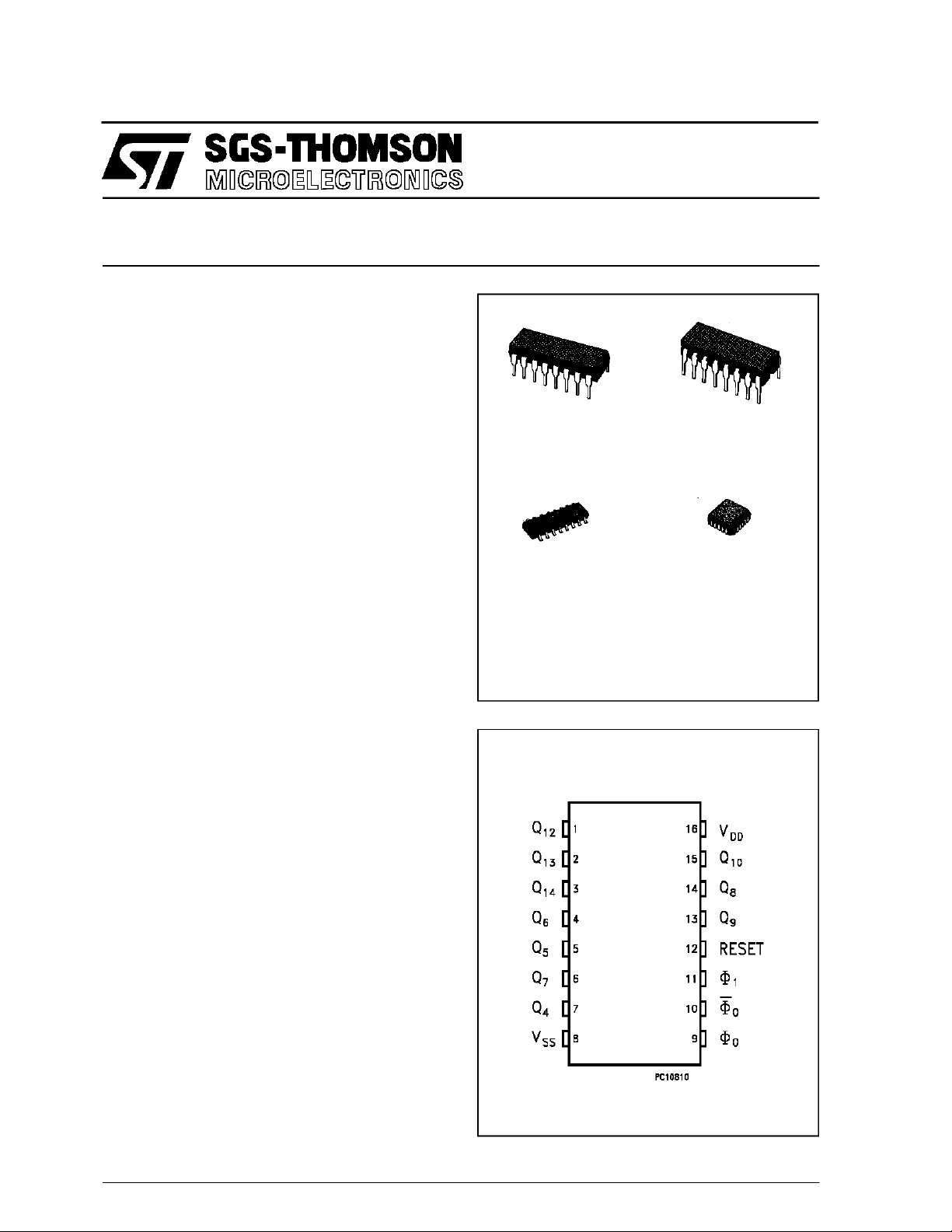
(PlasticPackage)
F
(CeramicPackage)
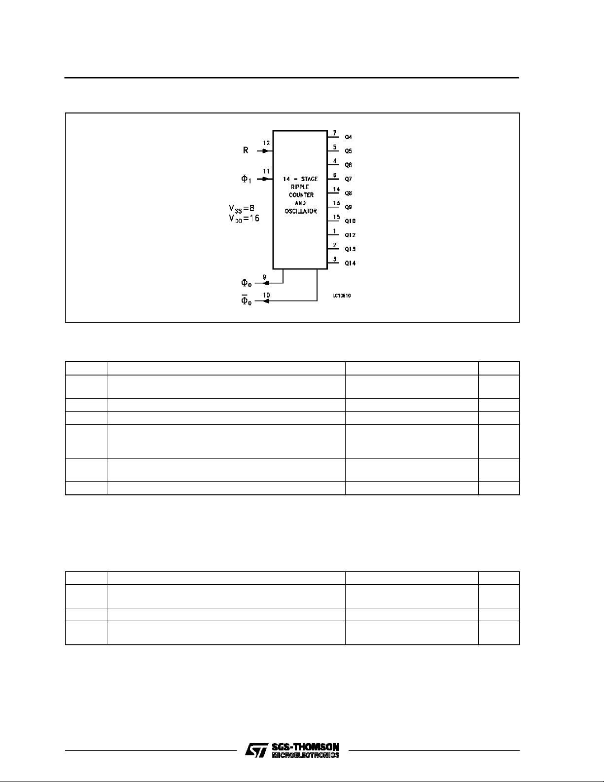
DESCRIPTION
TheHCC4060B (extended temperature range) and
HCF4060B (intermediate temperature range) are
monolithic integrated circuit, available in 16-lead
dual in line plastic or ceramic package and plastic
micropackage. The HCC/HCF4060B consist of an
oscillator sectionand 14 ripple carrybinary counter
stages.Theoscillator configuration allows design of
either RC or crystal oscillator circuits. A RESET
input is provided which reset the counter to the all
0’s state and disablesoscillator. A high level on the
RESET line accmplishes the reset function. All
counter stagesaremaster slaveflip-flops.The state
of the counter is advanced one stepin binaryorder
on the negative transition of φ1(and φ0). All inputs
and outputsare fully buffered.Schmitttriggeraction
on the clocklin permitsunlimited clock rise and fall
time.
M1
(MicroPackage)
ORDER CODES :
HCC4 060BF HCF4060BM1
HCF4060BEY HCF4060BC1
PIN CONNECTIONS
(Chip Carrier)
C1
September 1988
1/13
Page 2
HCC/HCF4060B
FUN CTIONAL DIAG R A M
ABSOLU TE MAXI MU M RAT ING
Symbol Parameter Value Unit
V
* Supply Voltage: HCC Types
DD
HCF Types
V
P
Input Voltage -0.5 to VDD+ 0.5 V
i
DC Input Current (any one input) ± 10 mA
I
I
Total Power Dissipation (per package)
tot
-0.5 to +20
-0.5 to +18
200
V
V
mW
Dissipation per Output Transistor
for Top = Full Package Temperature Range
T
Operating Temperature: HCC Types
op
HCF Types
T
Stressesabove those listedunder”AbsoluteMaximum Ratings”maycausepermanent damagetothedevice.Thisisastressratingonlyand functional
operation of the device at these or any otherconditions above thoseindicated in theoperational sections of thisspecificationisnotimplied.Exposure
to absolute maximum ratingconditionsforexternal periods mayaffect device reliability.
* All voltagevalues are referred to VSSpinvoltage.
Storage Temperature -65 to +150
stg
100
-55 to +125
-40 to +85
mW
o
C
o
C
o
C
RECO MM ENDED OPERAT IN G C O NDITIONS
Symbol Parameter Value Unit
V
V
T
Supply Voltage: HCC Types
DD
HCF Types
Input Voltage 0 to V
I
Operating Temperature: HCC Types
op
HCF Types
3to18
3to15
DD
-55 to +125
-40 to +85
V
V
V
o
C
o
C
2/13
Page 3
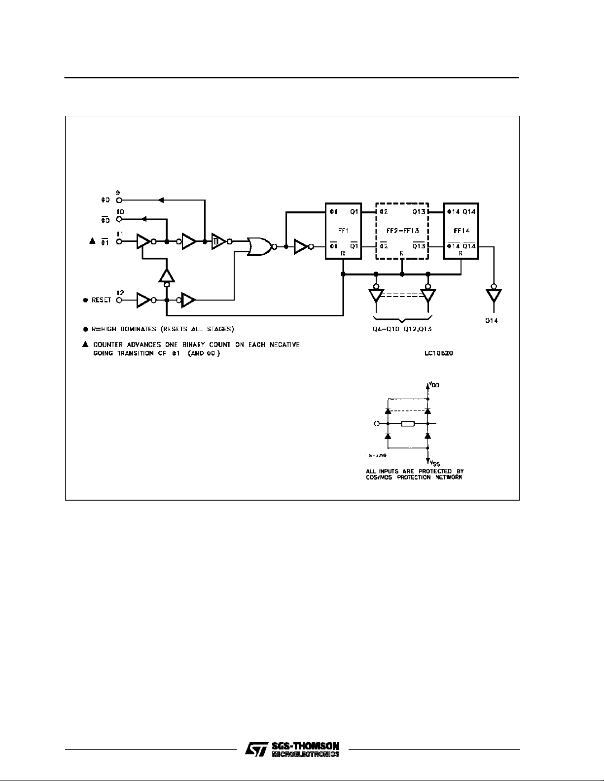
LOGI C DIAGRAM
HCC/HCF4060B
3/13
Page 4
HCC/HCF4060B
STATI C ELECT RIC AL CHA R ACTER IS TICS (over recommended op erating conditio ns)
Test Conditios Value
Symbol Parameter
Quiescent
I
L
Current
HCC
Types
V
(V)
V
I
(V)
|IO|
(µA)
V
(V)
O
T
DD
*25
LOW
Min. Max. Min. Typ. Max. Min. Max.
0/5 5 5 0.04 5 150
0/10 10 10 0.04 10 300
0/15 15 20 0.04 20 600
o
CT
0/20 20 100 0.08 100 3000
HCF
Types
0/5 5 20 0.04 20 150
0/10 10 40 0.04 40 300
0/15 15 80 0.04 80 600
OH
Output High
V
Voltage
0/5 < 1 5 4.95 4.95 4.95
0/10 < 1 10 9.95 9.95 9.95
0/15 < 1 15 14.95 14.95 14.95
OL
Output Low
V
Voltage
5/0 < 1 5 0.05 0.05 0.05
10/0 < 1 10 0.05 0.05 0.05
15/0 < 1 15 0.05 0.05 0.05
IH
Input High
V
Voltage
0.5/4.5 < 1 5 3.5 3.5 3.5
1/9 < 1 10 7 7 7
1.5/13.5 < 1 15 11 11 11
IL
Input Low
V
Voltage
4.5/0.5 < 1 5 1.5 1.5 1.5
9/1 < 1 10 3 3 3
13.5/1.5 < 1 15 4 4 4
OH
Output
Drive
Current
HCC
Types
I
0/5 2.5 5 -2 -1.6 -3.2 -1.15
0/5 4.6 5 -0.64 -0.51 -1 -0.36
0/10 9.5 10 -1.6 -1.3 -2.6 -0.9
0/15 13.5 15 -4.2 -3.4 -6.8 -2.4
0/5 2.5 5 -1.53 -1.36 -3.2 -1.1
HCF
Types
0/5 4.6 5 -0.52 -0.44 -1 -0.36
0/10 9.5 10 -1.3 -1.1 -2.6 -0.9
0/15 13.5 15 -3.6 -3.0 -6.8 -2.4
I
OL
Output
Sink
Current
HCC
Types
HCF
Types
0/5 0.4 5 0.64 0.51 1 0.36
0/10 0.5 10 1.6 1.3 2.6 0.9
0/15 1.5 15 4.2 3.4 6.8 2.4
0/5 0.4 5 0.52 0.44 1 0.36
0/10 0.5 10 1.3 1.1 2.6 0.9
0/15 1.5 15 3.6 3.0 6.8 2.4
I
IH,IIL
Input Leakage
Current
C
*T
LOW
*T
HIGH
TheNoiseMarginfor both ”1” and”0”level is: 1V min. withVDD=5V,2 V min.withVDD=10V,2.5 V min. withVDD=15V
Input Capacitance Any Input 5 7.5 pF
I
=-55oCforHCC device:-40oC for HCF device.
=+125oCfor HCCdevice:+85oC for HCF device.
0/18
0/15 15 ±0.3 ±10
Any Input
18 ±0.1 ±10-5±0.1 ±1 µA
-5
±0.3 ±1 µA
HIGH
Unit
*
µA
V
V
V
V
mA
mA
4/13
Page 5

HCC/HCF4060B
DYNAMIC ELECTRICAL CHARACTERISTICS (T
=25oC, CL=50pF,RL= 200 KΩ,
amb
typic al t emperature coeffic ent for all VDDvalues is 03 %/oC, all input rise and fall times = 20 ns )
Symbol Parameter
t
t
t
t
t
t
t
f
PLH
PHL
PLH
PHL
TLH
THL
t
r,tf
max
Propagation Delay Time
(φ to Q4 out)
Propagation Delay Time
(Qn to Q
n+1
)
Transition Time 5 100 200
Input Pulse Width f = 100KHz 5 50 100
W
Input Pulse Rise and Fall Time 5
Maximum Clock Input Frequency 5 3.5 7
RESET OPERATION
t
PHL
t
Propagation Delay Time 5 180 360
Reset Pulse Width 5 60 120
W
RC OPERATION
Variation of Frequency (Unit-to-Unit) C
Variation of Frequency With Voltage Change
(Same Unit)
R
X
C
X
Maximum Oscillator Frequency * R
* RC oscillatorapplications are notrecommended at supplyvoltages below 7V for RX=50KΩ
Test Conditions Value
(V) Min. Typ. Max.
V
DD
Unit
5 370 740
10 150 300
ns
15 100 200
5 100 200
10 50 100
ns
15 40 80
10 50 100
ns
15 40 80
10 20 40
ns
15 15 30
10
Unlimited µs
15
10 8 16
MHz
15 12 24
10 80 160
ns
15 50 100
10 30 60
ns
15 20 40
= 200pF
X
RS= 560KΩ
RX=50KΩ
= 200pF
C
X
RS= 560KΩ
RX=50KΩ
5 18 21.5 25
10 20 23 26
15 21.1 24 27
5to10 2
10to15 1
KHz
CX=10µF5 20
=50µF10 20
C
X
=10µF15 10
C
X
R
= 500 KΩ 5 1000
X
R
= 300 KΩ 10 50
X
R
= 300 KΩ 15 50
X
=5KΩ
X
CX= 15pF
10 530 650 810
15 690 800 94
MΩ
mF
pF
5/13
Page 6

HCC/HCF4060B
Typical Output Low (sink) Current Characteristics Minimum Output Low (sink) Current Charac-
teristics
Typical Output High (source) Current Characteristics
Minimum Output High (source) Current Characteristics
6/13
Page 7

DETAIL O F TY PICA L F I LP-FLO P STAGE
HCC/HCF4060B
TYPICAL RC OSILLA TOR C IRC UI T TYPICAL C RYSTAL O SCI LLA TOR CI R-
CUIT
7/13
Page 8

HCC/HCF4060B
TEST CIRCUITS
QuiescentDevice Current. Noise Immunity.
Input Leakage Current.
8/13
Page 9

Plastic DIP16 (0.25) MECHANICAL DATA
HCC/HCF4060B
DIM.
MIN. TYP. MAX. MIN. TYP. MAX.
a1 0.51 0.020
B 0.77 1.65 0.030 0.065
b 0.5 0.020
b1 0.25 0.010
D 20 0.787
E 8.5 0.335
e 2.54 0.100
e3 17.78 0.700
F 7.1 0.280
I 5.1 0.201
L 3.3 0.130
Z 1.27 0.050
mm inch
P001C
9/13
Page 10

HCC/HCF4060B
Ceramic DIP16/1 MECHANICAL DATA
DIM.
MIN. TYP. MAX. MIN. TYP. MAX.
A 20 0.787
B 7 0.276
D 3.3 0.130
E 0.38 0.015
e3 17.78 0.700
F 2.29 2.79 0.090 0.110
G 0.4 0.55 0.016 0.022
H 1.17 1.52 0.046 0.060
L 0.22 0.31 0.009 0.012
M 0.51 1.27 0.020 0.050
N 10.3 0.406
P 7.8 8.05 0.307 0.317
Q 5.08 0.200
mm inch
10/13
P053D
Page 11

SO16 (Narrow) MECHANICAL DATA
HCC/HCF4060B
DIM.
MIN. TYP. MAX. MIN. TYP. MAX.
A 1.75 0.068
a1 0.1 0.2 0.004 0.007
a2 1.65 0.064
b 0.35 0.46 0.013 0.018
b1 0.19 0.25 0.007 0.010
C 0.5 0.019
c1 45° (typ.)
D 9.8 10 0.385 0.393
E 5.8 6.2 0.228 0.244
e 1.27 0.050
e3 8.89 0.350
F 3.8 4.0 0.149 0.157
G 4.6 5.3 0.181 0.208
L 0.5 1.27 0.019 0.050
M 0.62 0.024
S8°(max.)
mm inch
P013H
11/13
Page 12

HCC/HCF4060B
PLCC20 MECHANICAL DATA
DIM.
MIN. TYP. MAX. MIN. TYP. MAX.
A 9.78 10.03 0.385 0.395
B 8.89 9.04 0.350 0.356
D 4.2 4.57 0.165 0.180
d1 2.54 0.100
d2 0.56 0.022
E 7.37 8.38 0.290 0.330
e 1.27 0.050
e3 5.08 0.200
F 0.38 0.015
G 0.101 0.004
M 1.27 0.050
M1 1.14 0.045
mm inch
12/13
P027A
Page 13

HCC/HCF4060B
Information furnished is believed to be accurate and reliable. However, SGS-THOMSON Microelectronics assumes no responsability forthe
consequences of use of such information nor for any infringement of patents or other rights of third parties which may results from its use. No
license is granted byimplicationor otherwise under any patentor patent rights ofSGS-THOMSON Microelectronics. Specificationsmentioned
in this publication aresubject to changewithout notice. This publication supersedes and replaces all information previously supplied.
SGS-THOMSON Microelectronicsproductsarenotauthorizedforuse ascriticalcomponentsinlifesupportdevicesorsystemswithoutexpress
written approval of SGS-THOMSON Microelectonics.
1994 SGS-THOMSON Microelectronics- All RightsReserved
Australia - Brazil - France - Germany - Hong Kong - Italy - Japan - Korea - Malaysia - Malta - Morocco - The Netherlands-
Singapore -Spain - Sweden - Switzerland - Taiwan - Thailand - UnitedKingdom - U.S.A
SGS-THOMSON Microelectronics GROUP OF COMPANIES
13/13
 Loading...