

Page 1
HCF4054B
4 SEGMENT LIQUID CRYSTAL DISPLAY
DRIVER WITH STROBED LATCH FUNCTION
■ QUIESCENT CURRENT SPECIF. UP TO 20V
■ OPERATION OF LIQUID CR YSTAL S WITH
CMOS CIRCUITS PROVIDES ULTRA LOW
POWER DISPLAYS
■ EQUIVALENT AC OUTPUT DRIVE FOR
LIQUID CRYSTAL DISPLAYS - NO
EXTERNAL CAPACITOR REQUIRED
■ VOLTAGE DOUBLING ACROSS DISPLAY
[(V
- VEE) = 18V] RESU LT S IN EFFECTIVE
DD
36V (p-p) DRIVE ACROSS SELECTED
DISPLAY SEGMENTS
■ LOW OR HIGH OUTPUT LEVEL DC DRIVE
FOR OTHER TYPES OF DISPLAYS
■ ONE CHIP LOGIC LEVEL CONVERSION
FOR DIFFERENT INPUT AND OUTPUT
LEVEL SWINGS
■ FULL DECODING OF ALL INPUT
COMBINATIONS : "0 - 9, L, H, P, A" AND
BLANK POSITIONS
■ INPUT LEAKAGE CURRENT
I
= 100nA (MAX) AT VDD = 18V TA = 25°C
I
■ 100% TESTED FOR QUIESCENT CURRENT
■ MEETS ALL REQUIREMENTS OF JEDEC
JESD13B "STANDARD SPECIFICATIONS
FOR DESCRIPTI ON OF B SERI ES CMOS
DEVICES"
DESCRIPTION
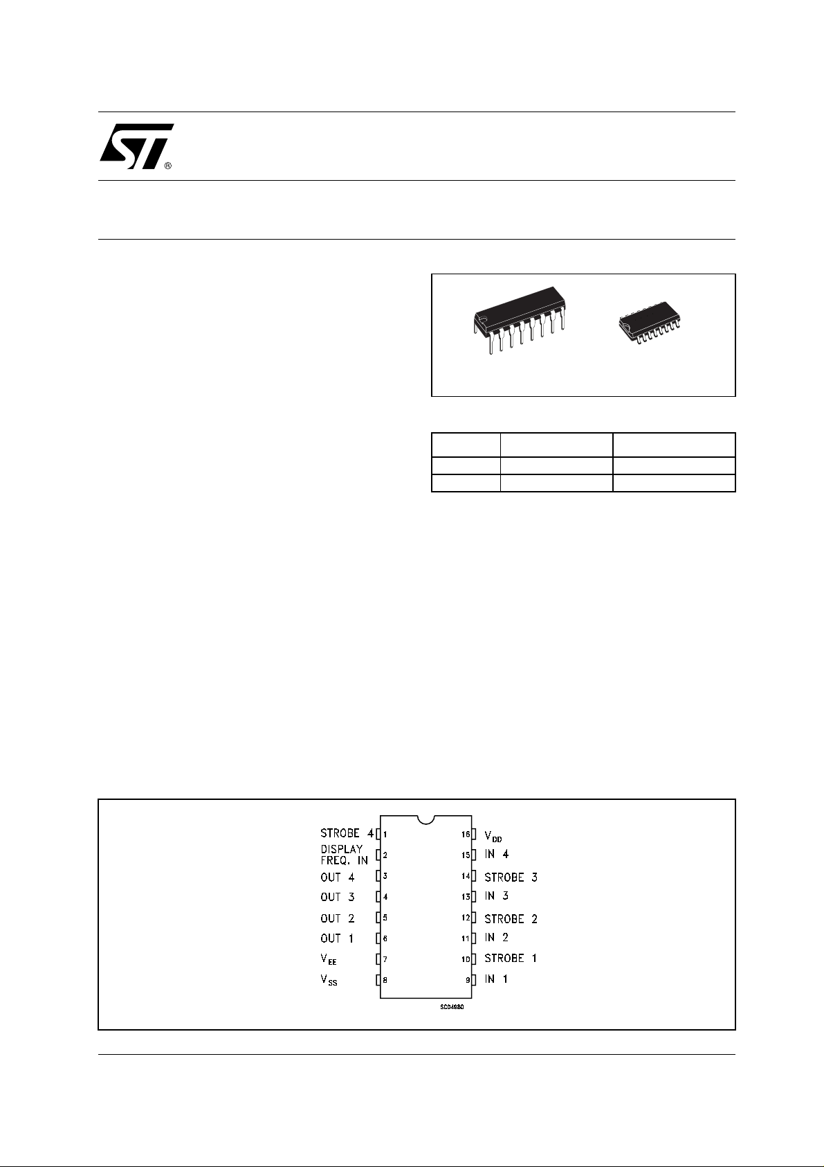
HCF4054B is a monolithic integrated circuit
fabricated in Metal Oxide Semiconductor
technology available in DIP and SOP packages.
DIP SOP
ORDER CODES
PACKAGE TUBE T & R
DIP HCF4054BEY
SOP HCF4054BM1 HCF4054M013TR
HCF4054B provides level shifting similar to
HCF4055B and HCF4056B, independently
strobed latches, and common DF control on 4
signal lines. This device is intended to provide
drive signal compatibility with HCF4055B and
HCF4056B 7-segment decoder types for the
decimal point, colon, polarity, and similar display
lines. A level-shifted high amplitude DF output can
be obtained from any HCF4054B output line by
connecting the corresponding input and strobe
lines to a low and high levels. HCF4054B may
also be utilized for logic level "up conversion" or
"down conversion" respectively. For example,
input signal swings (V
to VSS) from +5V to 0V
DD
PIN CONNECTION
1/11September 2002
Page 2
HCF4054B
can be converte d to outp ut signal swing s (VDD to
V
) of +5V to -5V. The level shifted function
EE
permits the use of different input and output signal
swings. The input swings from a low l evel of V
to a hi gh level of V
from a low level of V
V
. Thus, the input and output swings can be
DD
while the outputs swings
DD,
to the same high level of
EE
SS
selected independently of each ot her over a 3 to
18V range. V
may be connected to VEE when
SS
no level-shift function is required. Data is
transferred from input to output by placing a high
voltage level at the strobe input. A low voltage
level at the strobe input latches the data input and
the corresponding output segments remain
selected (or non selected) while the strobe is low.
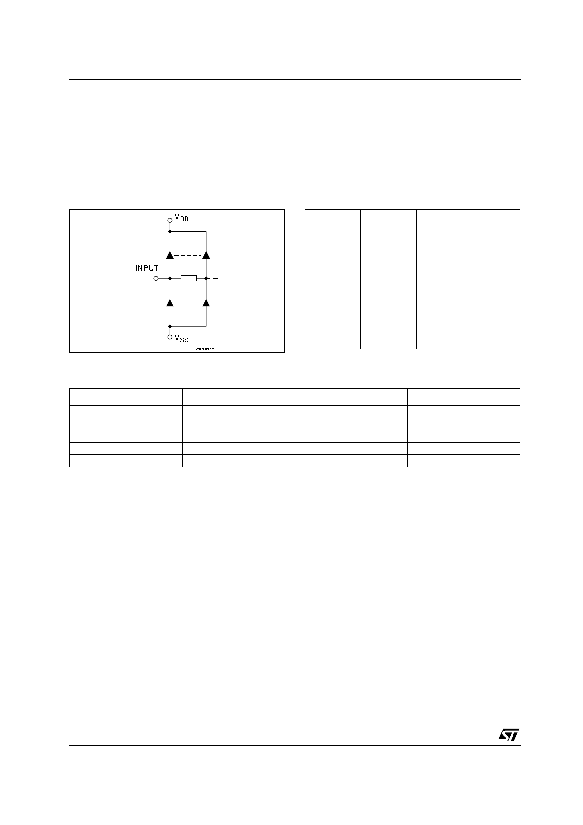
IINPUT EQUIVALENT CIRCUIT PIN DESCRIPTION
PIN No SYMBOL NAME AND FUNCTION
6, 5, 4, 3
9, 11, 13, 15 IN1 to IN4 Inputs
10, 12, 14, 1
2
7
8
16
OUT1 to
OUT4
STROBE1
STROBE4
DISPLAY
FREQ. IN
V
EE
V
SS
V
DD
TRUTH TABLE
Outputs
Strobe Input
Display Frequency Input
Negative Supply Voltage
Negative Supply Voltage
Positive Supply Voltage
DF IN STROBE OUT
LLHL
HLHH
LHHH
HHHL
XXL *
X = Don’t Care.
(*) Depe nds upon the input mode p reviously applied wh en S T =1.
2/11
Page 3
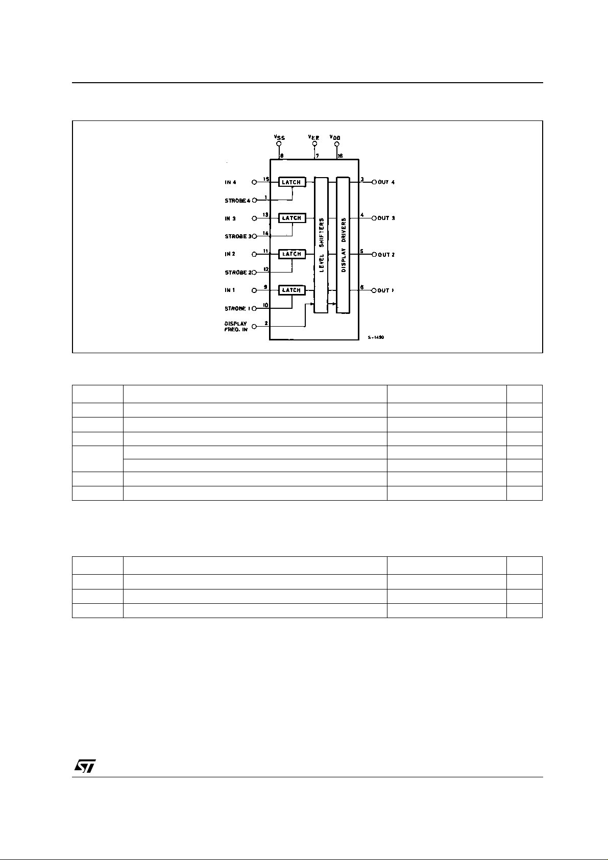
LOGIC DIAGRAM
HCF4054B
ABSOLUTE MAXIMUM RATINGS
Symbol Parameter Value Unit
V
V
P
Supply Voltage
DD
DC Input Voltage -0.5 to VDD + 0.5
I
I
DC Input Current
I
Power Dissipation per Package 200 mW
D
-0.5 to +22 V
10 mA
±
V
Power Dissipation per Output Transistor 100 mW
T
T
Absolute Maximum Ratings are those values beyond which damage to the device may occur. Functional operation under these conditions is
not implied.
All voltage value s are referred to V
Operating Temperature
op
Storage Temperature
stg
pin voltage.
SS
-55 to +125 °C
-65 to +150 °C
RECOMMENDED OPERATING CONDITIONS
Symbol Parameter Value Unit
V
V
T
Supply Voltage
DD
Input Voltage 0 to V
I
Operating Temperature
op
3 to 20 V
DD
-55 to 125 °C
V
3/11
Page 4
HCF4054B
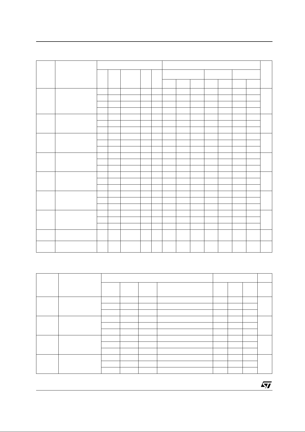
DC SPECIFICATIONS
Test Condition Value
T
Symbol Parameter
I
Quiescent Current -5 0/5 0 5 0.04 5 150 150
L
V
(V)
EE
V
V
(V)
SS
V
DD
(V)
V
I
(V)
O
(V)
= 25°C
A
Min. Typ. Max. Min. Max. Min. Max.
0 0/10 0 10 0.04 10 300 300
0 0/15 0 15 0.04 20 600 600
0 0/20 0 20 0.08 100 3000 3000
High Level Output
V
OH
Voltage
0 0/5 0 5 4.95 4.95 4.95
0 0/15 0 15 14.95 14.95 14.95
Low Level Output
V
OL
Voltage
0 5/0 0 5 0.05 0.05 0.05
0 15/0 0 15 0.05 0.05 0.05
High Level Input
V
IH
Voltage
-5 0.5/4.5 0 5 3.5 3.5 3.5
0 1.5/18.5 0 15 11 11 11
Low Level Input
V
IL
Voltage
5 0.5/4.5 0 5 1.5 1.5 1.5
0 1.5/18.5 0 15 4 4 4
I
OH
Output Drive
Current
-5 0/5 4.5 0 5 -0.38 -0.9 -0.28 -0.28
0 0/15 13.5 0 15 -1.27 -3 -0.95 -0.95
I
OL
Output Sink
Current
-5 0/5 0.4 0 5 1.1 2.6 0.82 0.82
0 0/15 1.5 0 15 2.9 6.8 2.17 2.17
Input Leakage
I
I
Current (any input)
C
Input Capacitance
I
(any input)
The Noi se Margin for both "1" a nd "0" level is: 1V min. wit h VDD=5V, 2V min. with VDD=10V, 2.5V min. with VDD=15V
0 0/18 0 18
-5
10
±
5 7.5 pF
-40 to 85°C -55 to 125°C
0.1
±
1
±
Unit
±1µ
A
µ
V0 0/10 0 10 9.95 9.95 9.95
V0 10/0 0 10 0.05 0.05 0.05
V01/90107 7 7
V09/1010 3 3 3
mA0 0/10 9.5 0 10 -0.38 -0.9 -0.28 -0.28
mA0 0/10 0.5 0 10 1.1 2.6 0.82 0.82
A
DYNAMIC ELECTRICAL CHARACTERISTICS (T
Test Condition Value (*) Unit
Symbol Parameter
V
EE
(V)
t
PHL tPLH
t
THL tTLH
Propagation Delay
Time (any Input to
any Output)
Transition Time
(any Output)
-5 0 5 400 800
0 0 15 250 500
-5 0 5 100 200
0 0 15 75 150
t
setup
Data Setup Time -5 0 5 220 110
0 0 15 70 35
Strobe Pulse Width -5 0 5 220 110
t
W
0 0 15 70 35
(*) Typical temper at ure coeffic i ent for all VDD value is 0.3 %/°C.
4/11
V
(V)
SS
V
(V)
= 25°C, CL = 50pF, RL = 200KΩ, tr = tf = 20 ns)
amb
DD
Min. Typ. Max.
ns0 0 10 340 680
ns0 0 10 100 200
ns0 0 10 100 50
ns0 0 10 100 50
Page 5
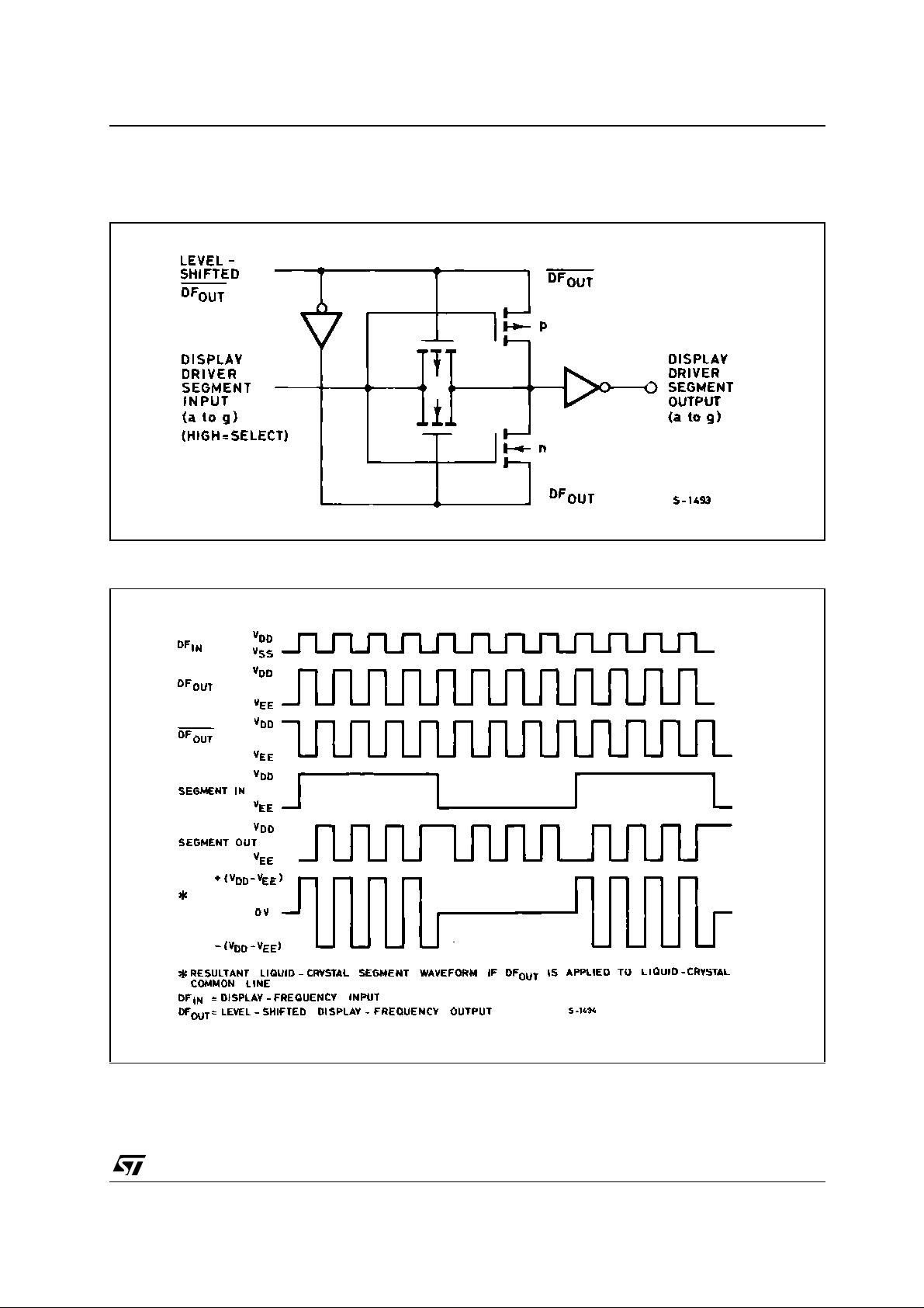
TYPICAL APPLICATIONS
Display Driver Circuit.
HCF4054B
Display Driver Waveform..
5/11
Page 6
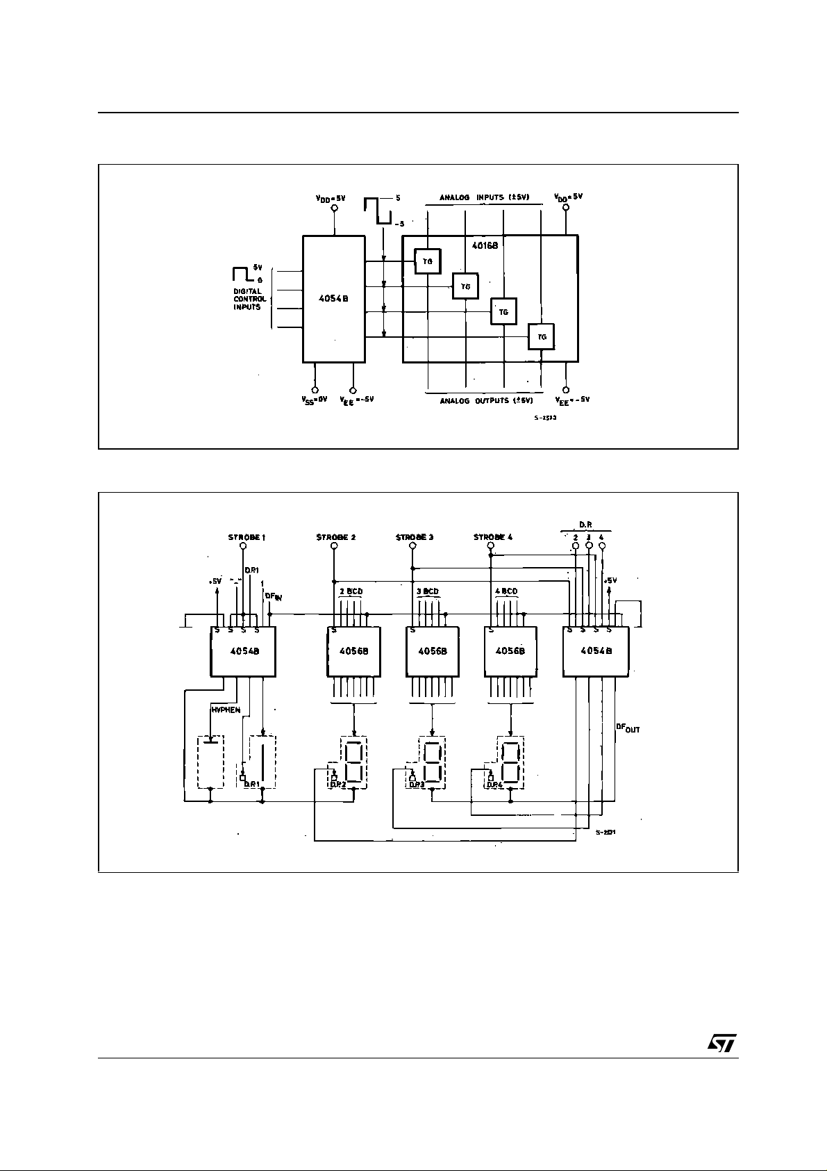
HCF4054B
Digital (0 to +5V) to Bidirectional Analog Control (+5V to -5V) Level Shifter.
Typical 3½ Digit Crystal Display : (V
= +5V, VSS = 0V, VEE = -10V, DFN = 30Hz Square)
DD
6/11
Page 7
HCF4054B
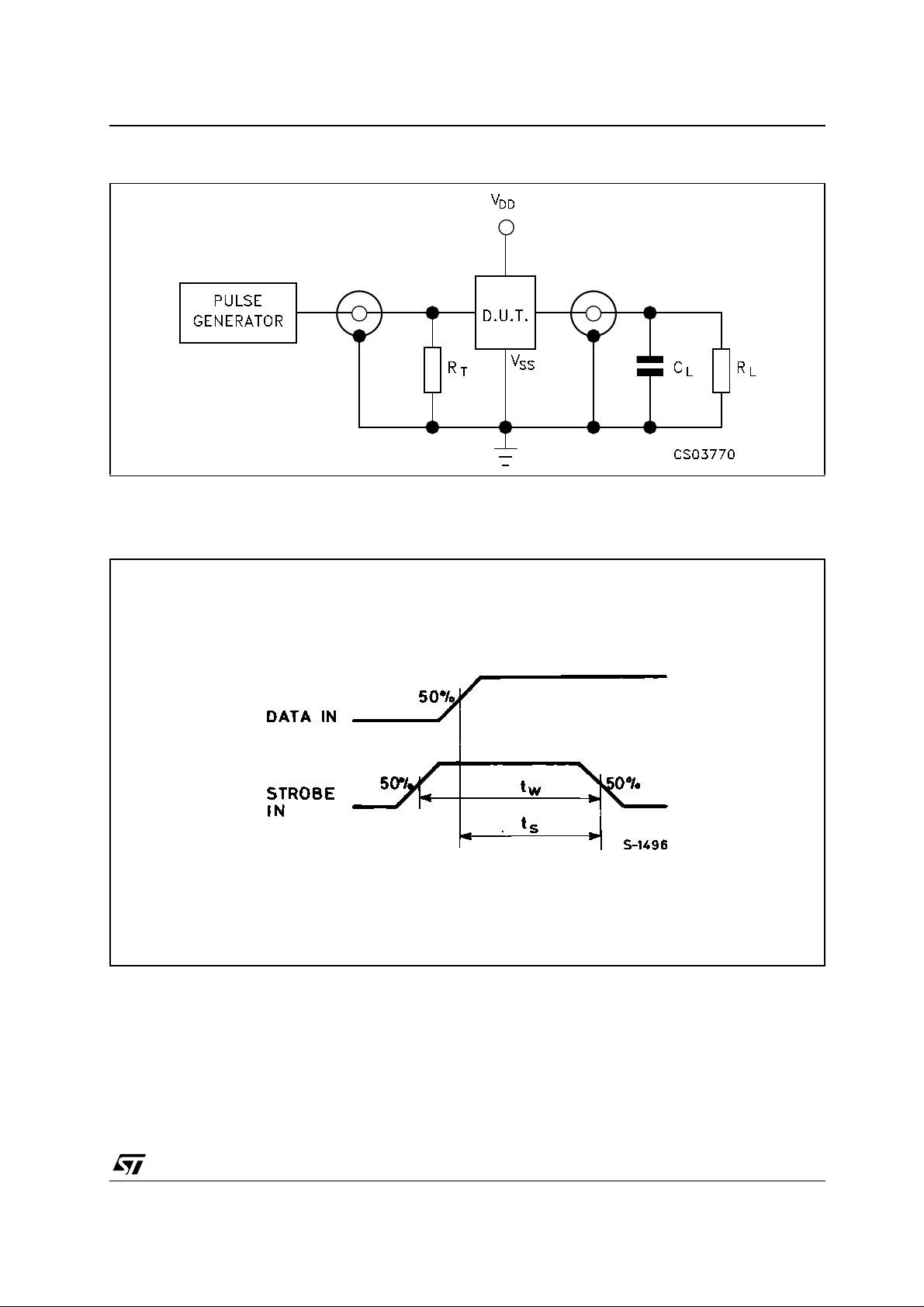
TEST CIRCUIT
CL = 50pF or equivalent (in cl udes jig and probe capac i tance)
R
= 200K
Ω
L
R
= Z
of pulse generator (typically 50Ω)
T
OUT
WAVEFORM : DATA SETUP TIME AND STROBE PULSE DURATION (f=1MHz; 50% duty cycle )
7/11
Page 8
HCF4054B
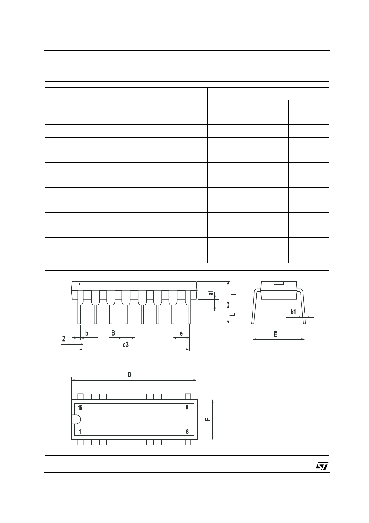
Plastic DIP-16 (0.25) MECHANICAL DATA
mm. inch
DIM.
MIN. TYP MAX. MIN. TYP. MAX.
a1 0.51 0.020
B 0.77 1.65 0.030 0.065
b 0.5 0.020
b1 0.25 0.010
D 20 0.787
E 8.5 0.335
e 2.54 0.100
e3 17.78 0.700
F 7.1 0.280
I 5.1 0.201
L 3.3 0.130
Z 1.27 0.050
8/11
P001C
Page 9
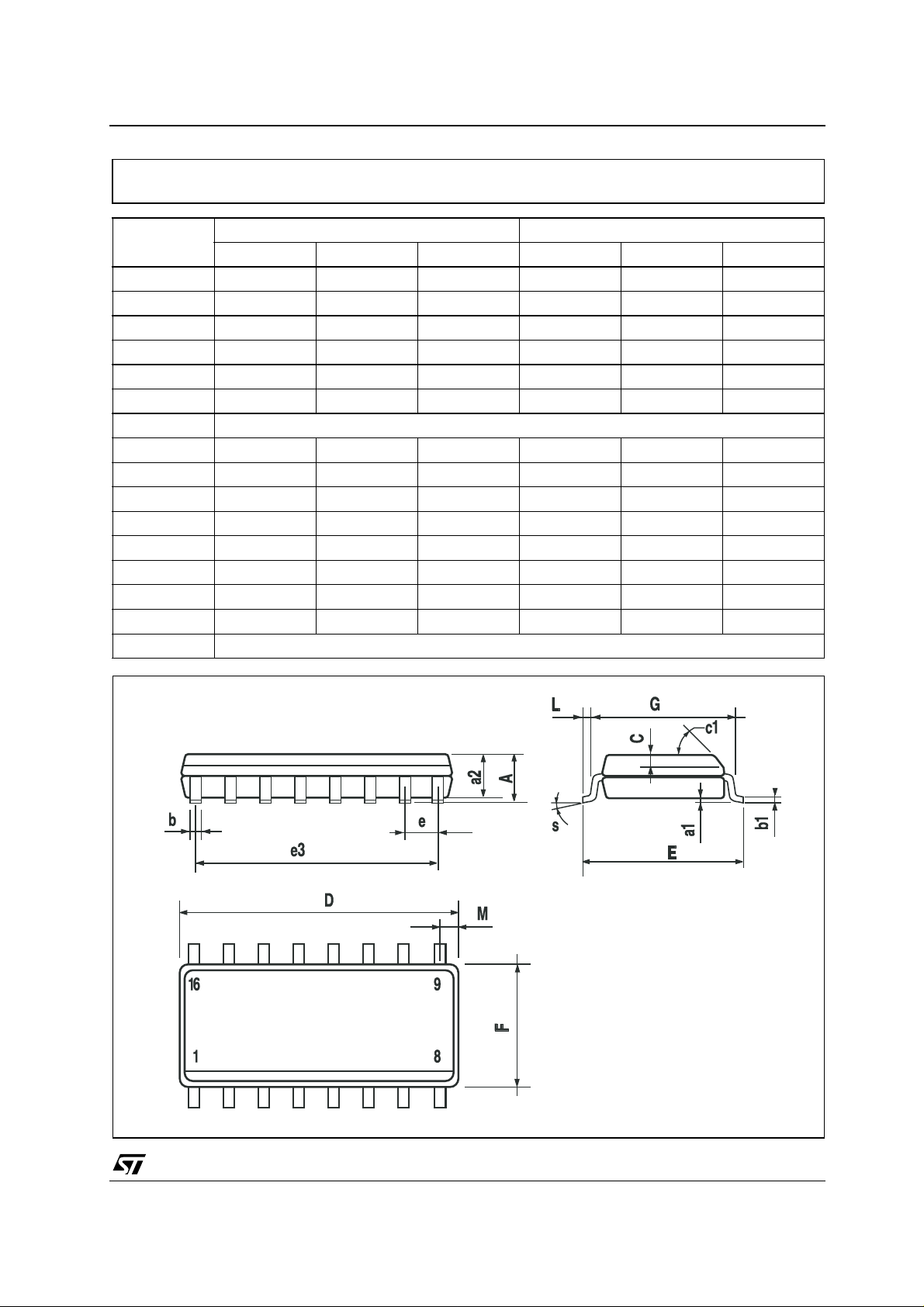
SO-16 MECHANICAL DATA
HCF4054B
DIM.
A 1.75 0.068
a1 0.1 0.2 0.003 0.007
a2 1.65 0.064
b 0.35 0.46 0.013 0.018
b1 0.19 0.25 0.007 0.010
C 0.5 0.019
c1 45˚ (typ.)
D 9.8 10 0.385 0.393
E 5.8 6.2 0.228 0.244
e 1.27 0.050
e3 8.89 0.350
F 3.8 4.0 0.149 0.157
G 4.6 5.3 0.181 0.208
L 0.5 1.27 0.019 0.050
M 0.62 0.024
S ˚ (max.)
MIN. TYP MAX. MIN. TYP. MAX.
mm. inch
8
PO13H
9/11
Page 10
HCF4054B
Information furnished is believed to be accurate and reliable. However, STMicroelectronics assumes no responsibi lity f or the
consequences of use of such informatio n nor for any infringement of paten ts or o ther rig hts of t hird part ies which ma y result from
its use. No license is granted by implication or otherwise under any patent or patent rights of STMicroelectronics. Specifications
mentioned in this publication are subject to change without notice. This publication supersedes and replaces all information
previousl y suppl ied. STM icroel ectronics produc ts are not auth orized for use as c ritica l compone nts in l ife s upport dev ices or
systems without express written approval of STMicroelectronics.
Australia - Brazil - Canada - China - Finland - France - Germany - Hong Kong - India - Israel - Italy - Japan - Malaysia - Malta - Morocco
© The ST logo is a registered trademark of STMicroelectronics
© 2002 STMicroelectronics - Printed in Italy - All Rights Reserved
STMicroelectronics GROUP OF COMPANIES
Singapore - Spain - Sweden - Switzerland - United Kingdom - United States.
© http://www.st.com
10/11
Page 11

HCF4054B
11/11
 Loading...