

Page 1
HCF4033B
DECADE COUNTER/DIVIDER WITH DECODED
7-SEGMENT DISPLAY OUTPUT AND RIPPLE BLANKING
■ COUNTER AND 7-SEGMENT DECODING IN
ONE PACKA GE
■ EASILY INTERFACED WITH 7-SEGMENT
DISPLAY TYPES
■ FULLY STATIC COUNTER OPERATION : DC
TO 6MHz (Typ.) AT V
■ IDEAL FOR LOW POWER DISPLAYS
■ RIPPLE BLANKI N G AND LAMP TEST
■ QUIESCENT CURRENT SPECIF. UP TO 20V
■ STANDARDIZED SYMMETRICAL OUTPUT
DD
= 10V
CHARACTERISTICS
■ INPUT LEAKAGE CURRENT
I
= 100nA (MAX) AT VDD = 18V TA = 25°C
I
■ 100% TESTED FOR QUIESCENT CURRENT
■ MEETS ALL REQUIREMENTS OF JEDEC
JESD13B " STANDARD SPECIFICATIONS
FOR DESCRIPTI ON OF B SERI ES CMOS
DEVICES"
DESCRIPTION
The HCF4033B is a m onolithic integrated circuit
fabricated in Metal Oxide Semiconductor
technology available in DIP and SOP packages.
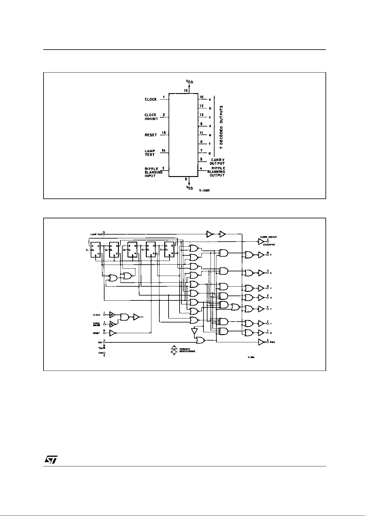
The HCF4033B consists of a 5-stages Johnson
decade counter and an output decoder which
converts the Johnson code to a 7 segment
decoded output for driving one stage in a
numerical display. This device is particularly
advantageous in display applications where low
power dissipation and/or low packag e count are
DIP SOP
ORDER CODES
PACKAGE TUBE T & R
DIP HCF4033BEY
SOP HCF4033BM1 HCF4033M013TR
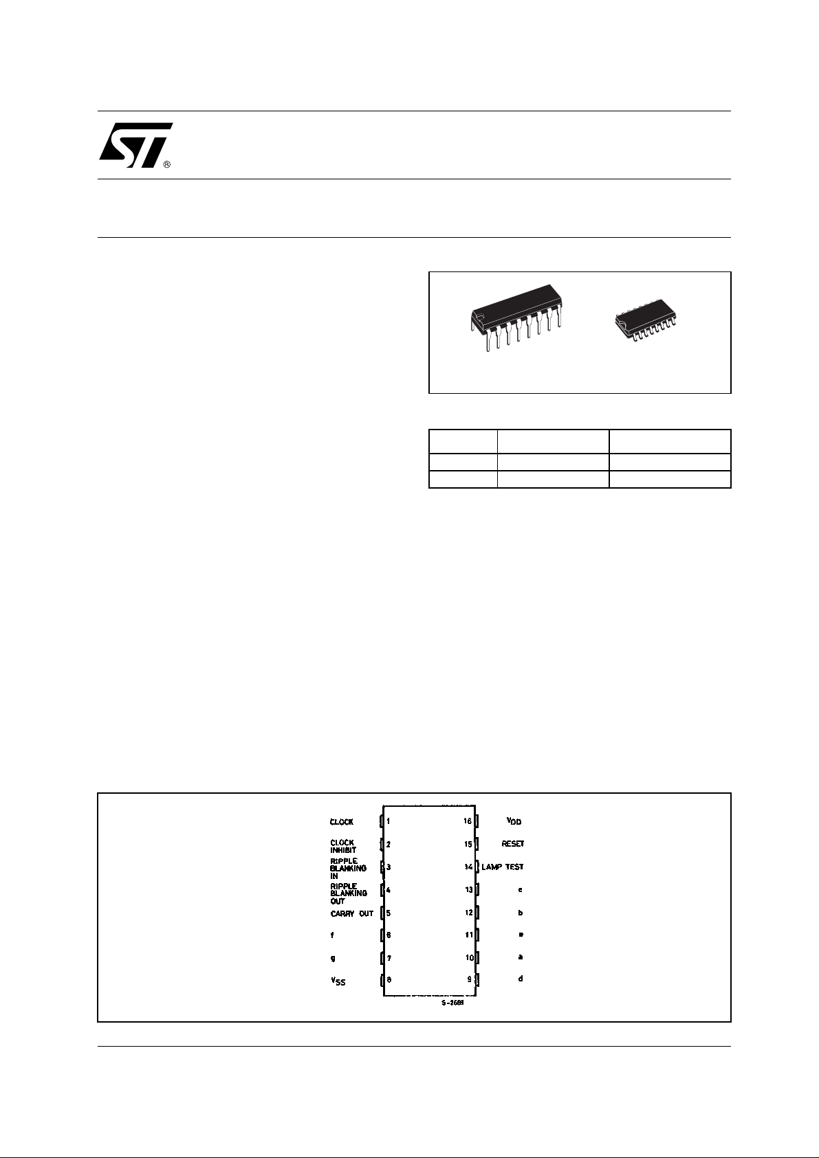
important. This device has CLOCK, RESET,
CLOCK INHIBIT, RIPPLE BLANKING, LAMP
TEST input, CARRY OUT, RIPPLE BLANKING
and 7 DECODED outputs (a to g).
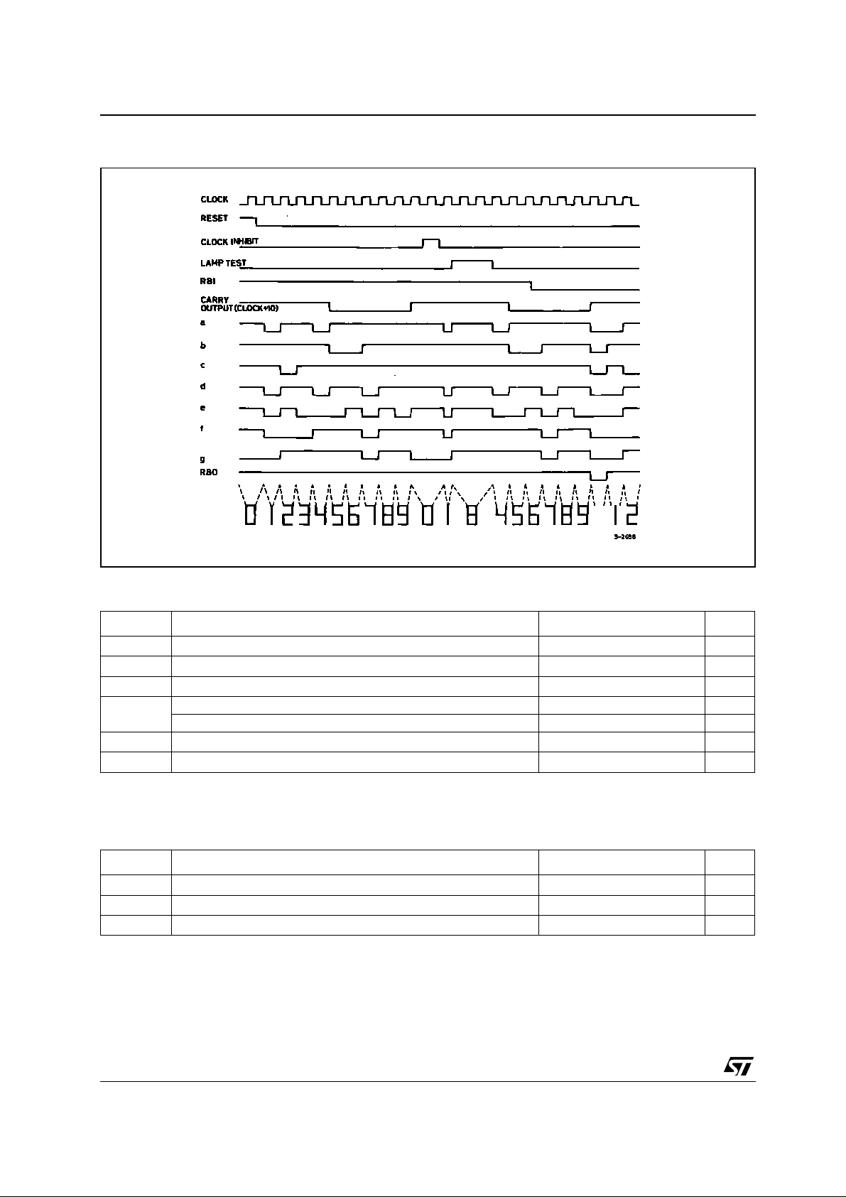
A high RESET signal clears the decade counter to
its zero count. The counter is advanced one count
at the positive clock signal transition if the CLOCK
INHIBIT signal is low. Counter advancem ent via
the clock line is inhibited when the CLOCK
INHIBIT signal is high. Antilock gating is provided
on the JOHN SON counter, thus assurin g proper
counting sequence. The CARRY-OUT (C
OUT
signal completes one cycle every ten CLOCK
INPUT cycles and is used to clock the succeeding
decade directly in a multi-decade counting chain.
)
PIN CONNECTION
1/11September 2001
Page 2
HCF4033B
The seven decoded outputs (a, b, c, d, e, f, g)
illuminate the proper segments in a seven
segment display device us ed for representing the
decimal numbers 0 to 9. The 7-segment outputs
go high on s election. This device has provisions
for automating blanking of the non-significant
zeros in a multi digit decimal number which results
in a easily readable display consistent with normal
writing practice. For example, the number
0050.07000 in an eight digit display would be
displayed as 50.07. Zero suppression on the
integer side is obtained by connecting the RBI
terminal of the HCF4033B associated with the
most significant digit in th e display to a low level
voltage and connecting the RBO terminal of that
stage to the RBI terminal of the HCF4033B in the
next lower significant position in the displ ay. This
procedure is continued for each succeeding
HCF4033B on the integer side o f the display. On
the fraction side of the display the RBI of the
HCF4033B associated with the least significant bit
is connected to a low level voltage and the RBO of
that HCF4033B is connected to the RBI terminal
of the HCF4033B i n the next more sign ificant bit
position. Again, this procedure is continued for all
HCF4033B’s on the fraction side of the display. In
a purely fractional number the zero immediately
preceding the decimal point can be displayed by
connecting the RBI of that stage to a high level
voltage (instead of to the RBO of the next more
significant stage). For example : optional zero →
0.7346. Likewise, the zero i n a number such as
763.0 can be displ ayed by connec ting the RBI of
the HCF4033B associated with it to a high leve l
voltage. Ripple blanking of non-significant zeros
provides an appreciable savings in display power.
The HCF4033B has a LAMP TES T input which,
when connected to a hi gh level vo ltage, ov errides
normal decoder operation and enables a ch eck to
be made on possible display malfunctions by
putting the seven outputs in the high state.
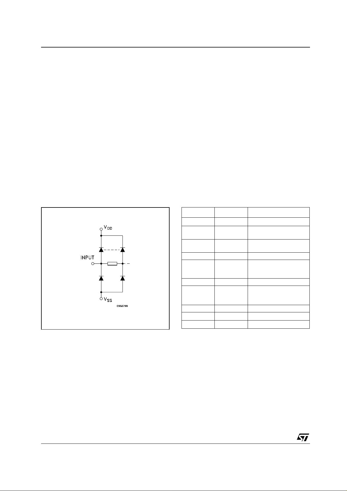
INPUT EQUIVALENT CIRCUIT PIN DESCRIPTION
PIN No SYMBOL NAME AND FUNCTION
1
10, 12, 13, 9,
11, 6, 7
2
15 RESET Reset Input
3
CLOCK
a to g
CLOCK
INHIBIT
RIPPLE
BLANKING INRipple Blanking Input
Clock Input
7 - Segments Decoded
Outputs
Clock Inhibit Input
2/11
5 CARRY OUT Carry Out Output
4
14 LAMP TEST Lamp Test Input
8
16
RIPPLE
BLANKING
OUT
V
SS
V
DD
Ripple Blanking Output
Negative Supply Voltage
Positive Supply Voltage
Page 3
FUNCTIONAL DIAGRAM
LOGIC DIAGRAM
HCF4033B
3/11
Page 4
HCF4033B
TIMING CHART
ABSOLUTE MAXIMUM RATINGS
Symbol Parameter Value Unit
V
V
P
Supply Voltage
DD
DC Input Voltage -0.5 to VDD + 0.5
I
I
DC Input Current
I
Power Dissipation per Package 200 mW
D
-0.5 to +22 V
± 10 mA
V
Power Dissipation per Output Transistor 100 mW
T
T
Absolute Maximum Ratings are those values beyond which damage to the device may occur. Functional operation under these conditions is
not implied.
All voltage values are referred to V
Operating Temperature
op
Storage Temperature
stg
pin voltage.
SS
-55 to +125 °C
-65 to +150 °C
RECOMMENDED OPERATING CONDITIONS
Symbol Parameter Value Unit
V
V
T
Supply Voltage
DD
Input Voltage 0 to V
I
Operating Temperature
op
3 to 20 V
DD
-55 to 125 °C
V
4/11
Page 5
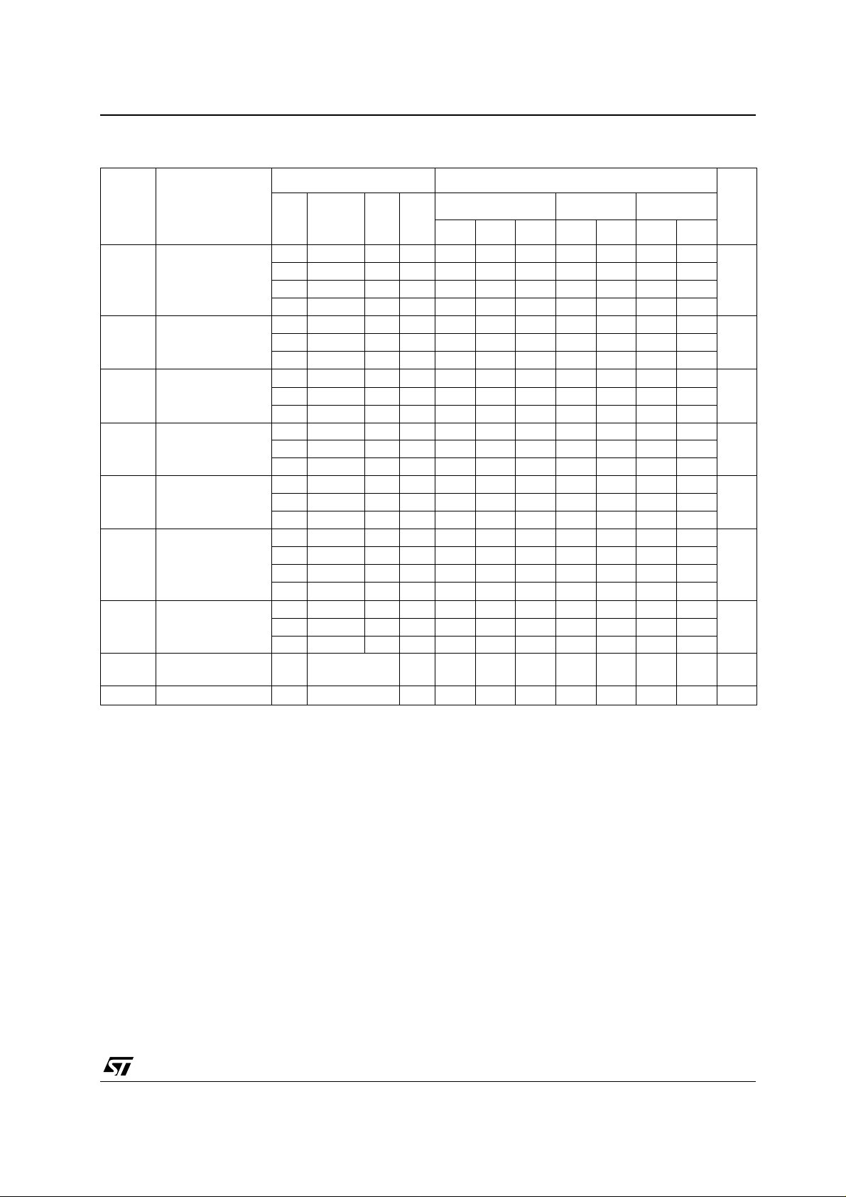
DC SPECIFICATIONS
Test Conditions Value
T
Symbol Parameter
I
Quiescent Current 0/5 5 0.04 5 150 150
L
V
(V)
V
I
I
O
(V)
O
(µA)
V
DD
(V)
= 25°C
A
Min. Typ. Max. Min. Max. Min. Max.
0/10 10 0.04 10 300 300
0/15 15 0.04 20 600 600
0/20 20 0.08 100 3000 3000
V
High Level Output
OH
Voltage
0/5 <1 5 4.95 4.95 4.95
0/15 <1 15 14.95 14.95 14.95
Low Level Output
V
OL
Voltage
5/0 <1 5 0.05 0.05 0.05
15/0 <1 15 0.05 0.05 0.05
High Level Input
V
IH
Voltage
0.5/4.5 <1 5 3.5 3.5 3.5
1.5/18.5 <1 15 11 11 11
V
IL
Low Level Input
Voltage
0.5/4.5 <1 5 1.5 1.5 1.5
1.5/18.5 <1 15 4 4 4
I
OH
Output Drive
Current
0/5 2.5 5 -1.36 -3.2 -1.1 -1.1
0/5 4.6 5 -0.44 -1 -0.36 -0.36
0/10 9.5 10 -1.1 -2.6 -0.9 -0.9
0/15 13.5 15 -3.0 -6.8 -2.4 -2.4
I
OL
Output Sink
Current
0/5 0.4 5 0.44 1 0.36 0.36
0/15 1.5 15 3.0 6.8 2.4 2.4
Input Leakage
I
I
Current
C
Input Capacitance
I
The Noi se Margin for bot h " 1" and "0" leve l is : 1 V mi n. with VDD=5V, 2V min. with VDD=10V, 2.5V min. with VDD=15V
0/18 any input 18
any input 5 7.5 pF
±10
-5
-40 to 85°C -55 to 125°C
±0.1 ±1 ± 1 µA
HCF4033B
Unit
µA
V0/10 <1 10 9.95 9.95 9.95
V10/0 <1 10 0.05 0.05 0.05
V1/9 <1 10 7 7 7
V9/1 <1 10 3 3 3
mA
mA0/10 0.5 10 1.1 2.6 0.9 0.9
5/11
Page 6
HCF4033B
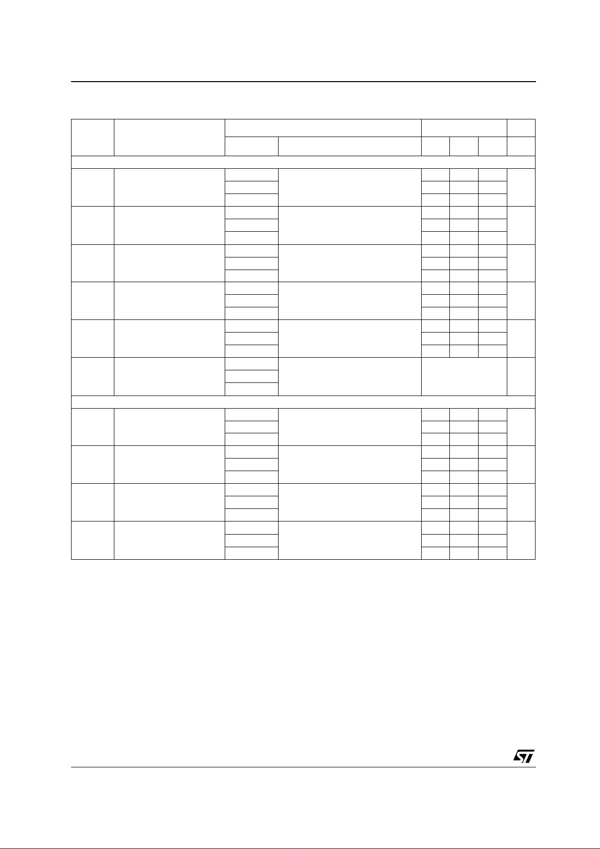
DYNAMIC ELECTRICAL CHARACTERISTICS (T
Symbol Parameter
CLOCKED OPERATION
t
PLH tPHL
t
PLH tPHL
t
THL tTLH
f
CL
t
t
Propagation Delay Time
(Carry Out Line)
Propagation Delay Time
(Decoded Out Lines)
Transition Time
(Carry Out Line)
(1)
Maximum Clock Input
Frequency
Clock Pulse Width 5 110 260
WC
Clock Input Rise or Fall
, t
r
f
Time
RESET OPERATION
t
PLH tPHL
t
PLH tPHL
t
t
(*) Typical temperature coefficient for all VDD value is 0.3 %/°C.
(1) Measured with respect to carry output line.
Propagation Delay Time
(Carry Out Line)
Propagation Delay Time
(Decoded Out Lines)
Reset Pulse Widht 5 100 120
WR
Reset Removal Time 5 0 30
rem
(V)
V
DD
5 250 500
15 75 150
5 350 700
15 90 180
5 100 200
15 25 50
5 2.5 5
15 8 16
15 40 80
5
15
5 275 550
15 80 160
5 300 600
15 90 180
15 25 50
15 0 10
= 25°C, CL = 50pF, RL = 200KΩ, tr = tf = 20 ns)
amb
Test Condition Value (*) Unit
Min. Typ. Max.
ns10 100 200
ns10 125 250
ns10 50 100
MHz10 5.5 11
ns10 50 100
Unlimited µs10
ns10 120 240
ns10 125 250
ns10 50 100
ns10 0 15
6/11
Page 7
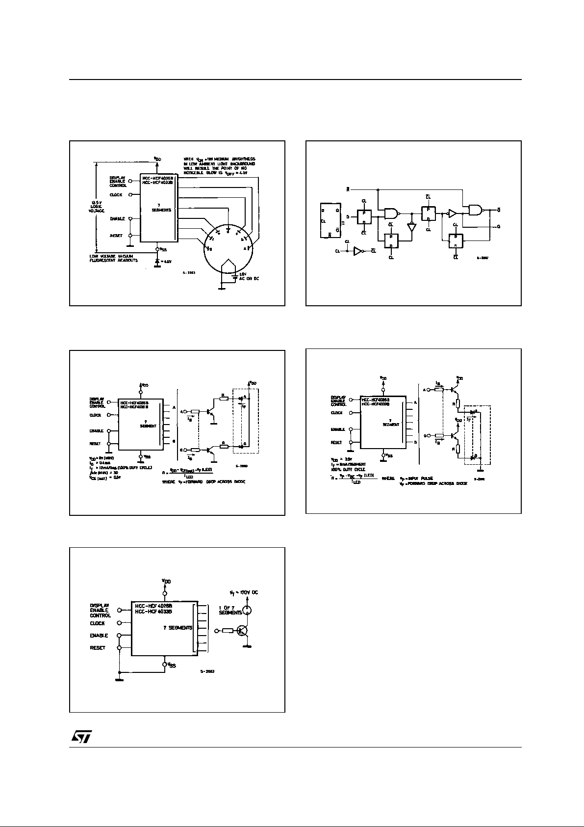
TYPICAL APPLICATIONS
HCF4033B
Interfacing with Filament Fluorescent Display
Interfacing with LED Displays (display common
anode)
Detail of Typical Flip-flop Stage
Interfacing with LED Displays (display common
cathode)
Interfacing with NIXIE Tube
7/11
Page 8
HCF4033B
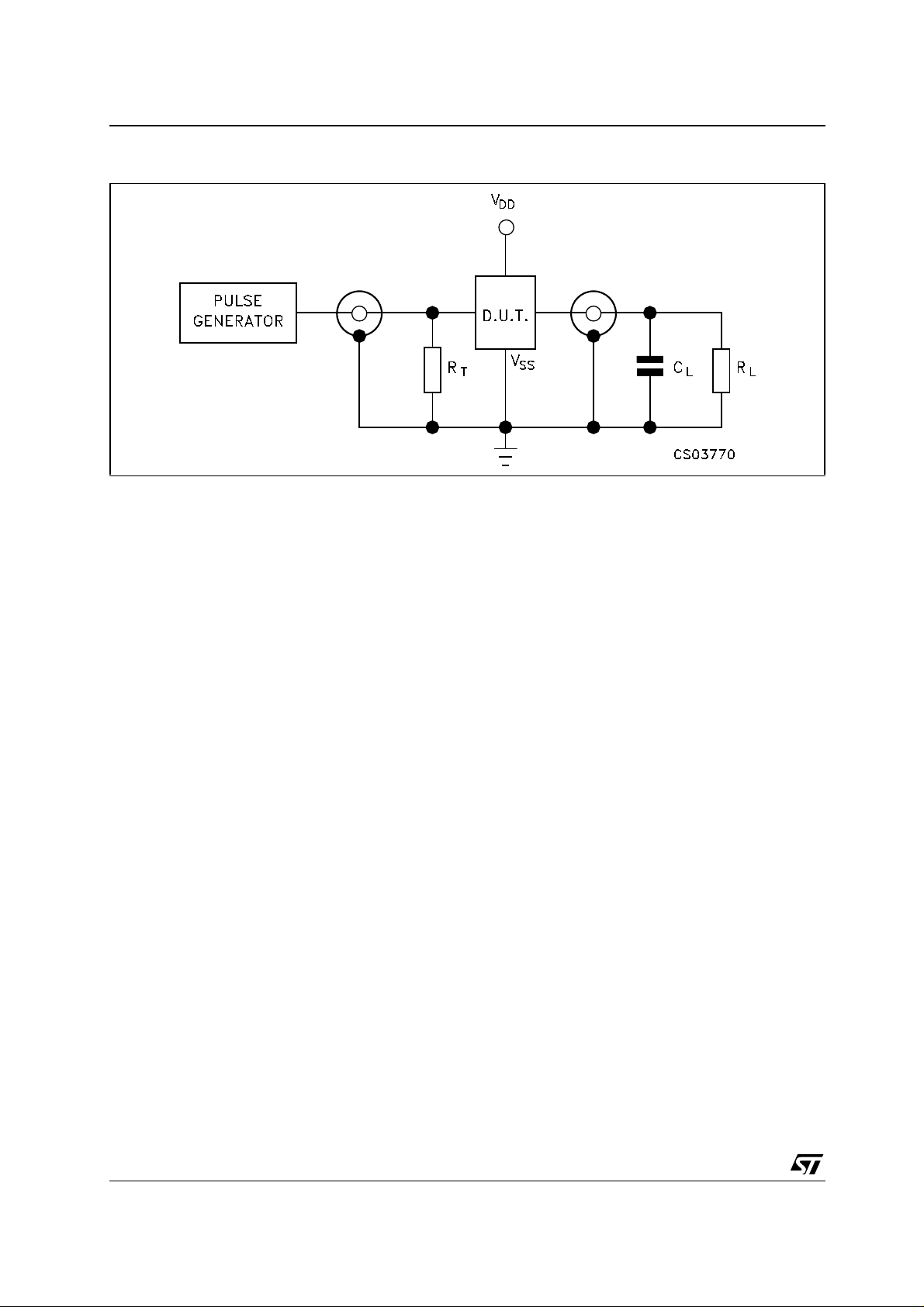
TEST CIRCUIT
CL = 50pF or equivalent (includes jig and prob e capacitance)
= 200KΩ
R
L
R
= Z
of pulse generator (typically 50Ω)
T
OUT
8/11
Page 9
HCF4033B
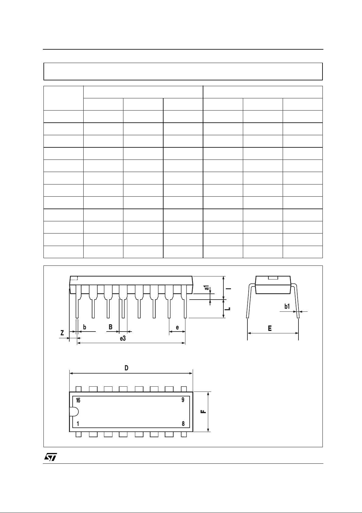
Plastic DIP-16 (0.25) MECHANICAL DATA
mm. inch
DIM.
MIN. TYP MAX. MIN. TYP. MAX.
a1 0.51 0.020
B 0.77 1.65 0.030 0.065
b 0.5 0.020
b1 0.25 0.010
D 20 0.787
E 8.5 0.335
e 2.54 0.100
e3 17.78 0.700
F 7.1 0.280
I 5.1 0.201
L 3.3 0.130
Z 1.27 0.050
P001C
9/11
Page 10
HCF4033B
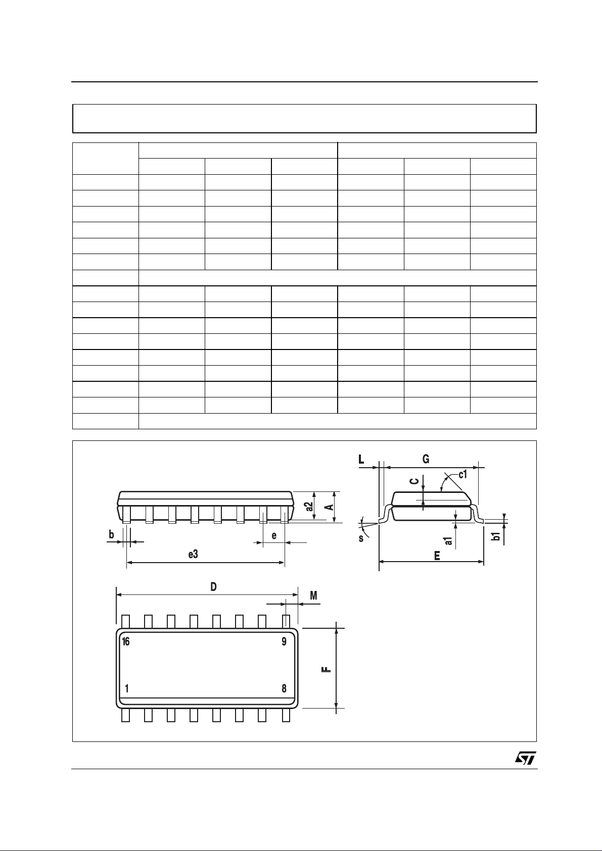
SO-16 MECHANICAL DATA
DIM.
A 1.75 0.068
a1 0.1 0.2 0.003 0.007
a2 1.65 0.064
b 0.35 0.46 0.013 0.018
b1 0.19 0.25 0.007 0.010
C 0.5 0.019
c1 45° (typ.)
D 9.8 10 0.385 0.393
E 5.8 6.2 0.228 0.244
e 1.27 0.050
e3 8.89 0.350
F 3.8 4.0 0.149 0.157
G 4.6 5.3 0.181 0.208
L 0.5 1.27 0.019 0.050
M 0.62 0.024
S8° (max.)
MIN. TYP MAX. MIN. TYP. MAX.
mm. inch
10/11
PO13H
Page 11

HCF4033B
Information furnished is bel ieved to be accurate and reliable. However, STMicroe lectronics assumes no responsibility for the
consequences of use of such information nor for any infringement of patents or other rights of third parties which may result from
its use. No li cense is granted by implication or otherwise under any pat ent or patent rights of STMicroelec tronics. Specifications
mentioned in this publication ar e subject to change without notice. This publication supersedes and replaces all information
previously supplied. S TMicroelectronics products are not authorized for use as critica l components in life suppo rt devices or
systems without express written approval of STMicroelectronics.
Australi a - Brazil - China - Finland - Fra nce - Germany - Ho ng Kong - India - Italy - Japan - Mal aysia - Malta - Mo rocco
© The ST logo is a registered trademark of STMicroelectronics
© 2001 STM icroelectr o n ics - Printed in Italy - All Rights Reserved
STMicr o el ectronics GROU P OF COM P ANIES
Singapo re - Spain - Sweden - Switzerland - United K i ngdom
© http://www.st.com
11/11
 Loading...