

Page 1
HCF40192B
PRESETTABLE UP/DOWN COUNTER
(DUAL CLOCK WITH RESET) BCD TYPE
■ INDIVIDUAL CLOCK LINES FOR COUNTING
UP OR COUNTING DOWN
■ SYNCHRONOUS HIGH-SPEED CARRY AND
BORROW PROPAGATION DELAYS FOR
CASCADING
■ ASYNCHRONOUS RESET AND PRESET
CAPABILITY
■ MEDIUM-SPEED OPERATION - f
= 8MHz
CL
(typ.) AT 10 V
■ STANDARDIZED SYMMETRICAL OUTPUT
CHARACTERISTICS
■ QUIESCENT CURRENT SPECIF . UP TO 20V
■ 5V , 10V AND 15V PARAMETRIC RAT INGS
■ INPUT LEAKAGE CURRENT
I
= 100nA (MAX) AT VDD = 18V TA = 25°C
I
■ 100% TESTED FOR QUIESCENT CURRENT
■ MEETS ALL REQUIREMENTS OF JEDEC
JESD13B "STANDARD SPECIFICATIONS
FOR DESCRIPTI ON OF B SERI ES CMOS
DEVICES"
DESCRIPTION
HCF40192B is a monolithic integrated circuit
fabricated in Metal Oxide Semiconductor
technology available in DIP and SOP packages.
HCF40192B Presettable BCD Up /Down Counter
consists of 4 synchronou sly clocked, GATE D "D"
type flip-flops connected as a counter. The inputs
consist of four individual jam lines, a PRESET
ENABLE control, individual CLOCK UP and
CLOCK DOWN signals and a master RESET.
Four buffered Q signal outputs, as well as CARRY
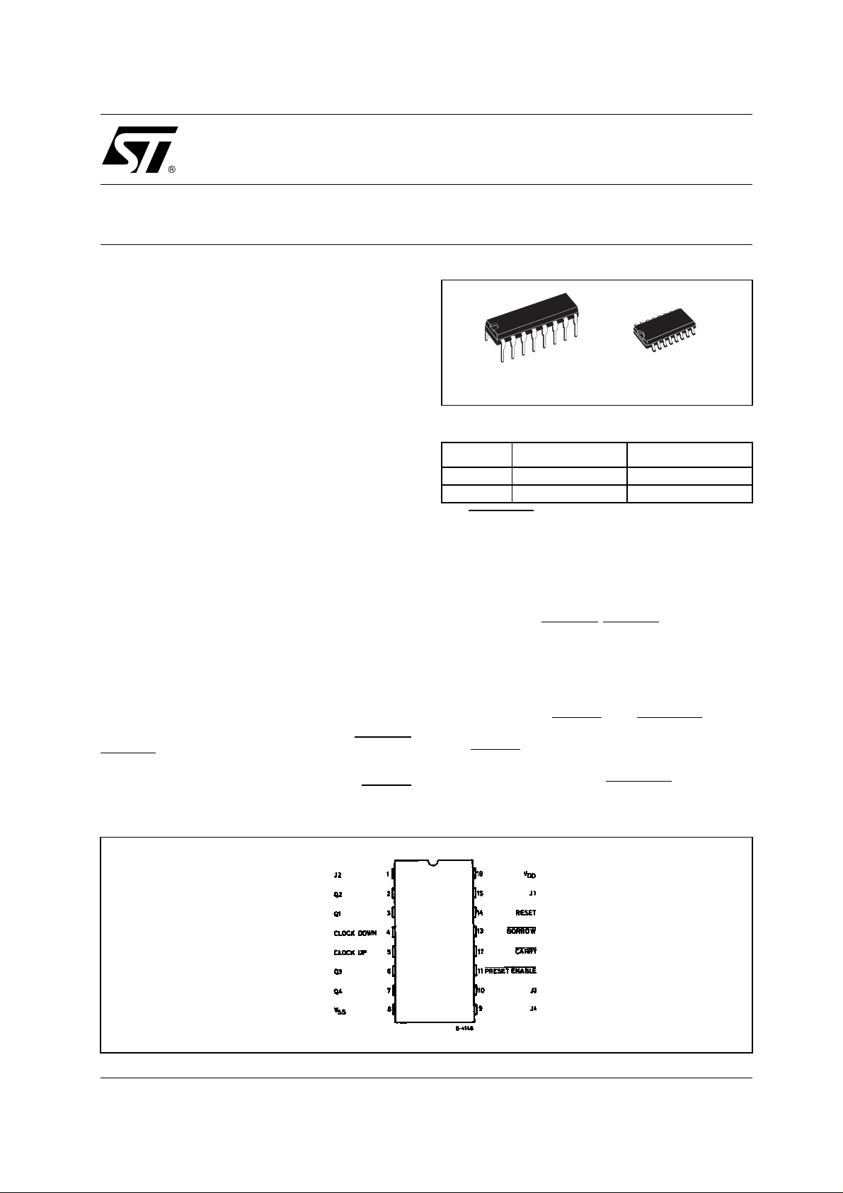
DIP SOP
ORDER CODES
PACKAGE TUBE T & R
DIP HCF40192BEY
SOP HCF40192BM1 HCF40192M013TR
and BORROW outputs for multiple-stage counting
schemes, are provided . The count er is c lea red so
that all outputs are in a l ow st ate by a high on the
RESET line. A RESET is accomplished
asynchronously with the clock. Each output is
individually programmable asynchronously with
the clock to the level on the corresponding jam
input when the P RESET
ENABLE control is low .
The counter counts up one count on the positive
clock edge of the CLOCK UP s ignal, provid ed the
CLOCK DOWN l ine is hig h. The counter counts
down one count on the posit ive clock edg e of the
CLOCK DOWN signal provided the CLOCK UP
line is high. The CARRY
and BORROW signals
are high when the counter is counts up or down.
The CARRY
signal goes low one-half clock cycle
after the counter reaches its maximum count in
the count-up mode. The BORROW
signal goes
PIN CONNECTION
1/12September 2002
Page 2
HCF40192B
low one-half clock cycle after the counter reaches
its minimum count in the count-down mod e. The
cascading of multiple packages is easily
accomplished without the need for additional
external circuitry by tying the BORROW
CARRY
outputs to the CLOCK DOWN and
CLOCK UP inpu ts, respectively, of the following
package.
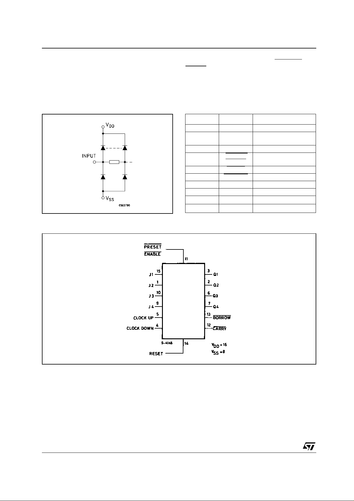
IINPUT EQUIVALENT CIRCUIT PIN DESCRIPTION
PIN No SYMBOL NAME AND FUNCTION
3, 2, 6, 7 Q1 to Q4 Flip-Flop Outputs
4
5 CLOCK UP Clock Up Input
11
12 CARRY
13 BORROW
14 RESET Reset Input
15, 1, 10, 9 J1 to J4 Data Input
8
16
CLOCK
DOWN
PRESET
ENABLE
V
SS
V
DD
FUNCTIONAL DIAGRAM
and
Clock Down Input
Preset Enable Input
Count Up (Carry)
Count Down (Borrow)
Negative Supply Voltage
Positive Supply Voltage
2/12
Page 3
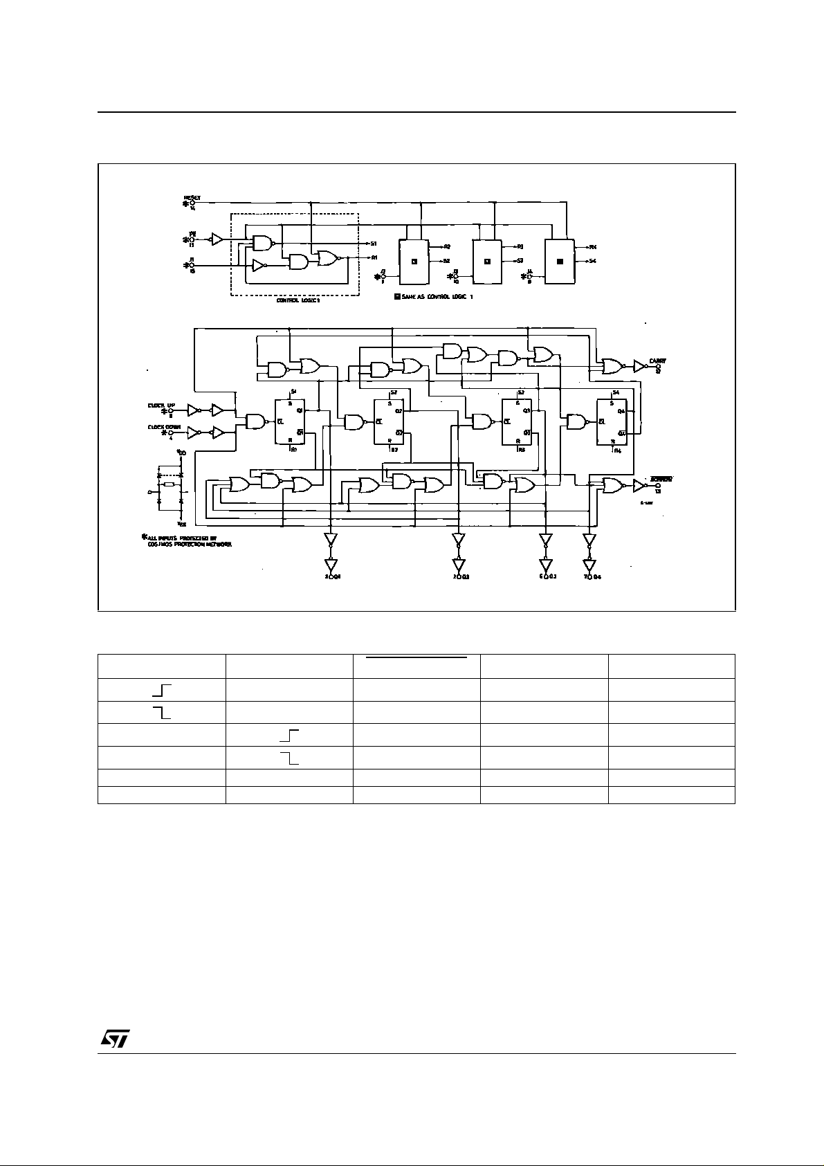
LOGIC DIAGRAM
HCF40192B
TRUTH TABLE
CLOCK UP CLOCK DOWN PRESET ENABLE RESET ACTION
H H L COUNT UP
H H L NO COUNT
H H L COUNT DOWN
H H L NO COUNT
X X L L PRESET
XXXHRESET
(X) : Don’t Care
3/12
Page 4
HCF40192B
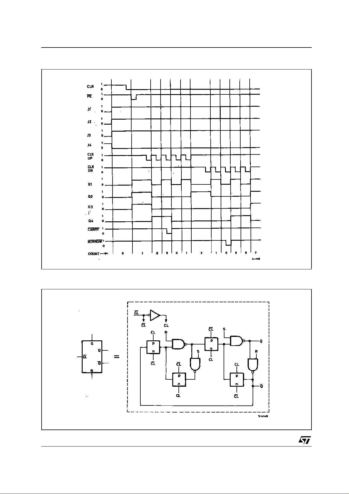
TIMING DIAGRAM
INTERNAL LOGIC FLIP-FLOP
4/12
Page 5
HCF40192B
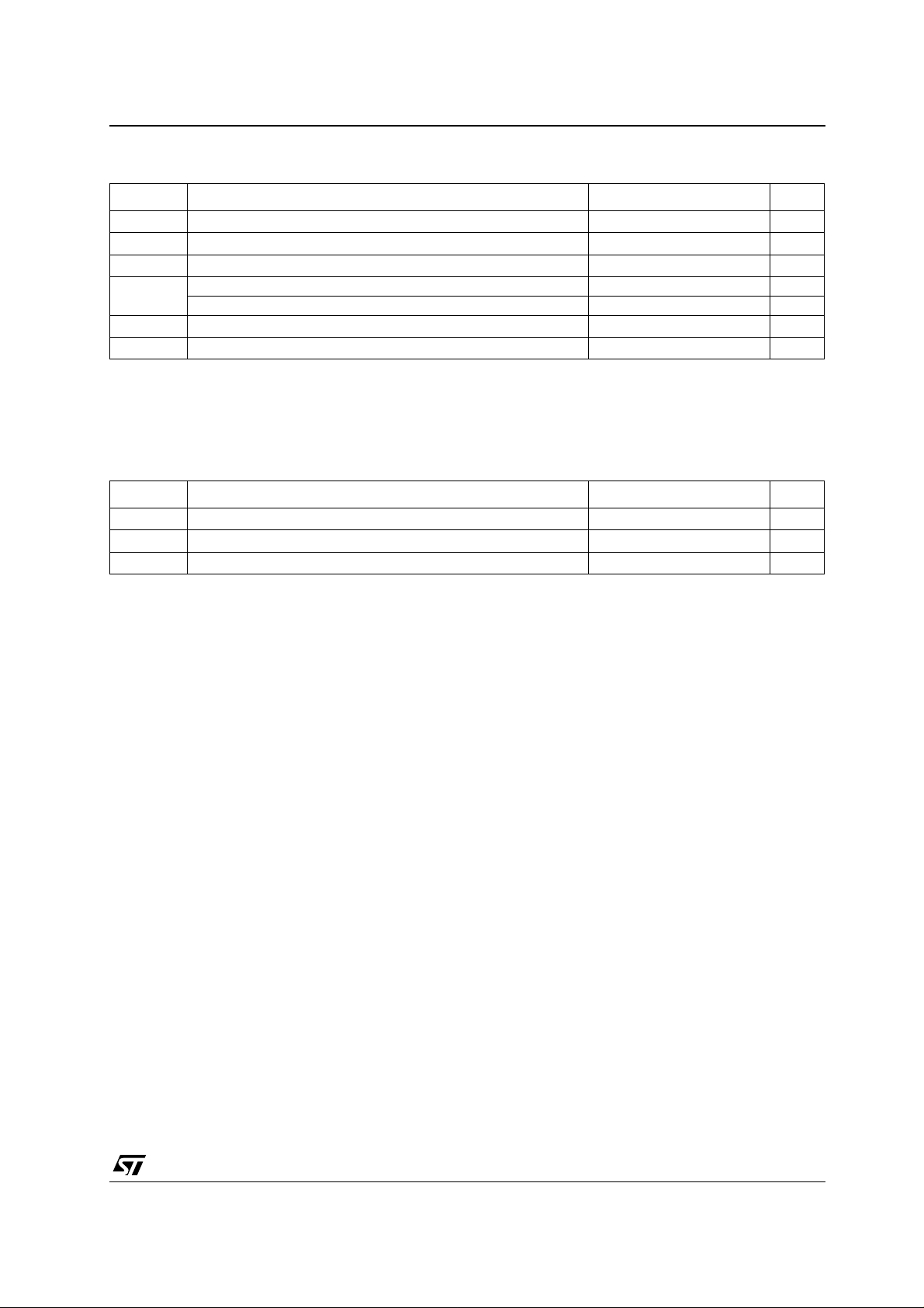
ABSOLUTE MAXIMUM RATINGS
Symbol Parameter Value Unit
V
V
P
T
T
Absolute Maximum Ratings are those values beyond which damage to the device may occur. Functional operation under these conditions is
not implied.
All voltage value s are referr ed to V
RECOMMENDED OPERATING CONDITIONS
Symbol Parameter Value Unit
V
V
T
Supply Voltage
DD
DC Input Voltage -0.5 to VDD + 0.5
I
I
DC Input Current
I
Power Dissipation per Package 200 mW
D
-0.5 to +22 V
10 mA
±
Power Dissipation per Output Transistor 100 mW
Operating Temperature
op
Storage Temperature
stg
pin voltage.
SS
Supply Voltage
DD
Input Voltage 0 to V
I
Operating Temperature
op
-55 to +125 °C
-65 to +150 °C
3 to 20 V
DD
-55 to 125 °C
V
V
5/12
Page 6
HCF40192B
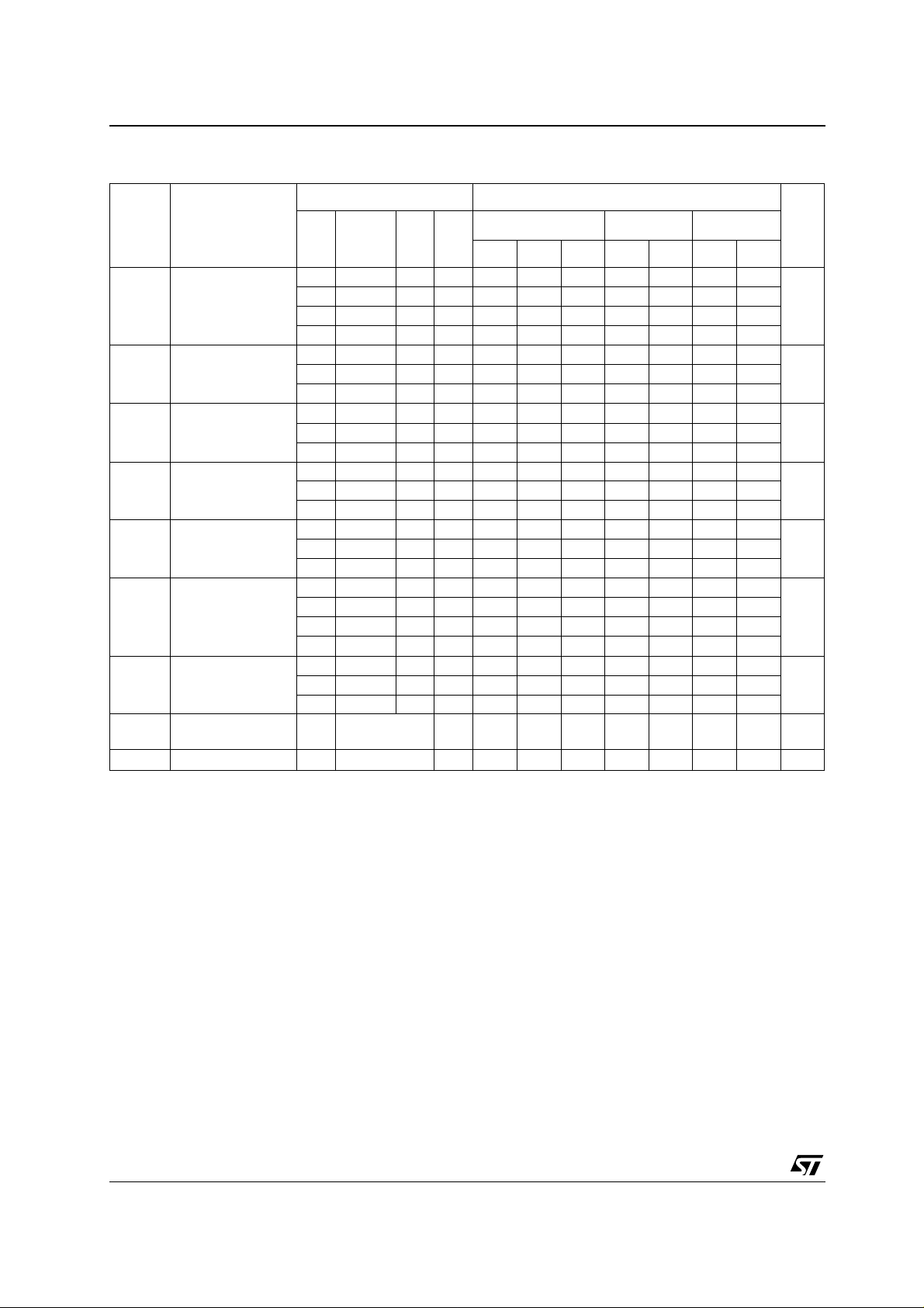
DC SPECIFICATIONS
Test Condition Value
T
Symbol Parameter
I
Quiescent Current 0/5 5 0.04 5 150 150
L
V
(V)
V
I
(V)
|I
|
O
O
(µA)
V
DD
(V)
= 25°C
A
Min. Typ. Max. Min. Max. Min. Max.
0/10 10 0.04 10 300 300
0/15 15 0.04 20 600 600
0/20 20 0.08 100 3000 3000
V
High Level Output
OH
Voltage
0/5 <1 5 4.95 4.95 4.95
0/15 <1 15 14.95 14.95 14.95
Low Level Output
V
OL
Voltage
5/0 <1 5 0.05 0.05 0.05
15/0 <1 15 0.05 0.05 0.05
High Level Input
V
IH
Voltage
0.5/4.5 <1 5 3.5 3.5 3.5
1.5/13.5 <1 15 11 11 11
V
IL
Low Level Input
Voltage
4.5/0.5 <1 5 1.5 1.5 1.5
13.5/1.5 <1 15 4 4 4
I
OH
Output Drive
Current
0/5 2.5 <1 5 -1.36 -3.2 -1.1 -1.1
0/5 4.6 <1 5 -0.44 -1 -0.36 -0.36
0/10 9.5 <1 10 -1.1 -2.6 -0.9 -0.9
0/15 13.5 <1 15 -3.0 -6.8 -2.4 -2.4
I
OL
Output Sink
Current
0/5 0.4 <1 5 0.44 1 0.36 0.36
0/15 1.5 <1 15 3.0 6.8 2.4 2.4
Input Leakage
I
I
Current
C
Input Capacitance
I
The Noi se Margin for both "1" and " 0" level is: 1V min. with VDD=5V, 2V min. with VDD=10V, 2.5V min. with VDD=15V
0/18 Any Input 18
Any Input 5 7.5 pF
-5
10
±
-40 to 85°C -55 to 125°C
0.1
±
1
±
Unit
A
µ
V0/10 <1 10 9.95 9.95 9.95
V10/0 <1 10 0.05 0.05 0.05
V1/9 <1 10 7 7 7
V9/1 <1 10 3 3 3
mA
mA0/10 0.5 <1 10 1.1 2.6 0.9 0.9
1
±
A
µ
6/12
Page 7
HCF40192B
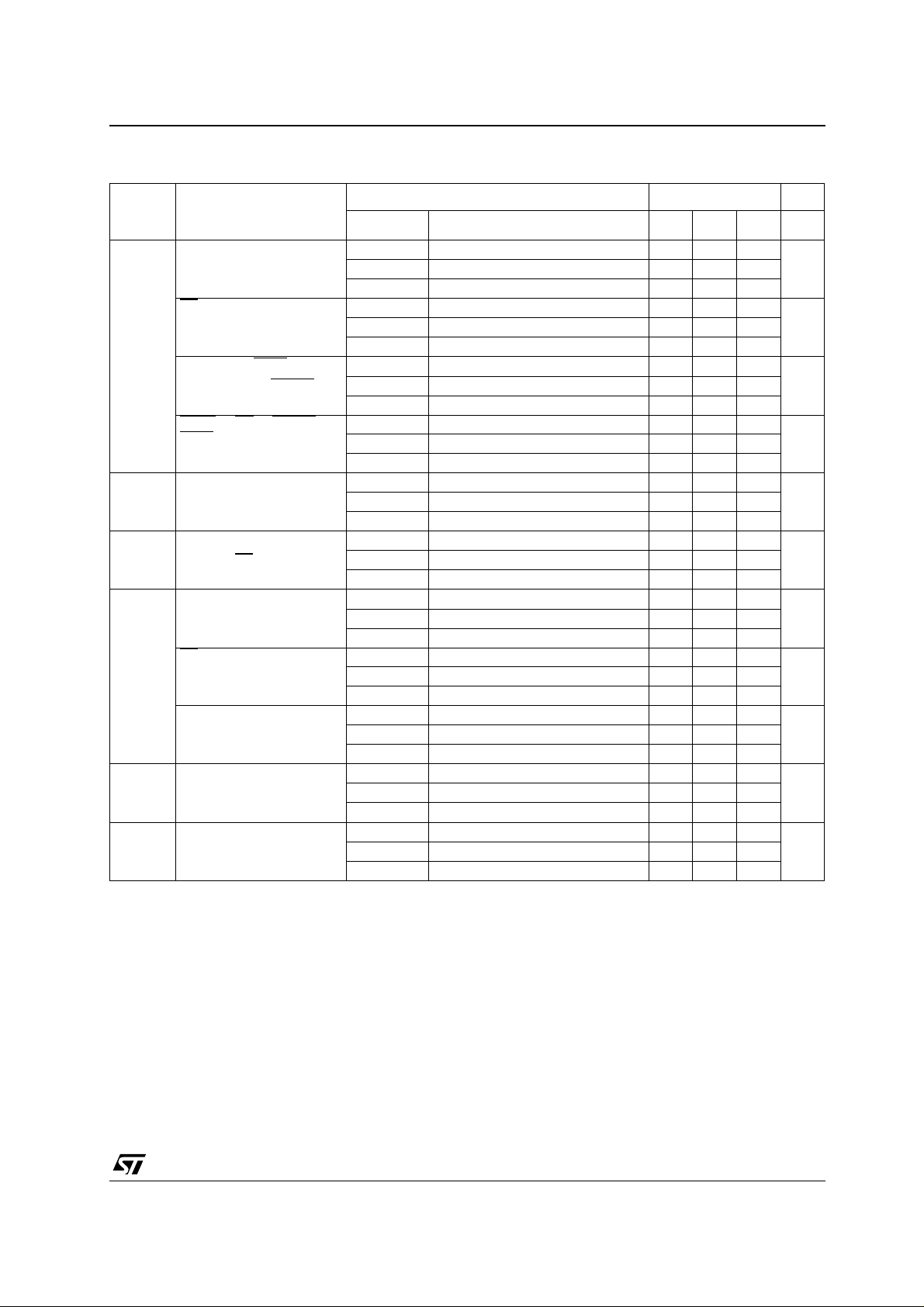
DYNAMIC ELECTRICAL CHARACTERISTICS (T
= 25°C, CL = 50pF, RL = 200KΩ, tr = tf = 20 ns)
amb
Test Condition Value (*) Unit
Symbol Parameter
t
PLH tPHL
Propagation Delay Time
Clock Up or Clock Down to
Q Reset to Q
to Q 5 200 400
PE
(V)
V
DD
5 250 500
15 90 180
15 70 140
Clock Up to Carry
Clock Down to Borrow
5 160 320
15 60 120
or PR to Borrow or
Reset
5 300 600
Carry
15 110 220
t
THL tTLH
Transition Time 5 100 200
15 40 80
t
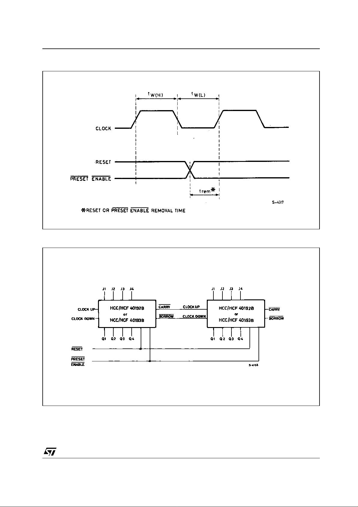
rem*
Removal Time
58040
Reset or PE
15 30 15
Clock Input Pulse Width
t
W
Reset
5 480 240
15 260 130
PE
5 120 240
15 70 140
Clock 5 90 180
15 30 60
t
Clock Input Rise or Fall
r tf
Time
515
15 5
Maximum Clock Input
f
CL
Frequency
524
15 5.5 11
(*) The time required for Reset or Preset Enable control to be removed before clocking (see timing diagram).
Min. Typ. Max.
ns10 120 240
ns10 100 200
ns10 80 160
ns10 150 300
ns10 50 100
ns10 40 20
ns10 300 150
ns10 85 170
ns10 45 90
µs10 15
MHz10 5 8
7/12
Page 8
HCF40192B
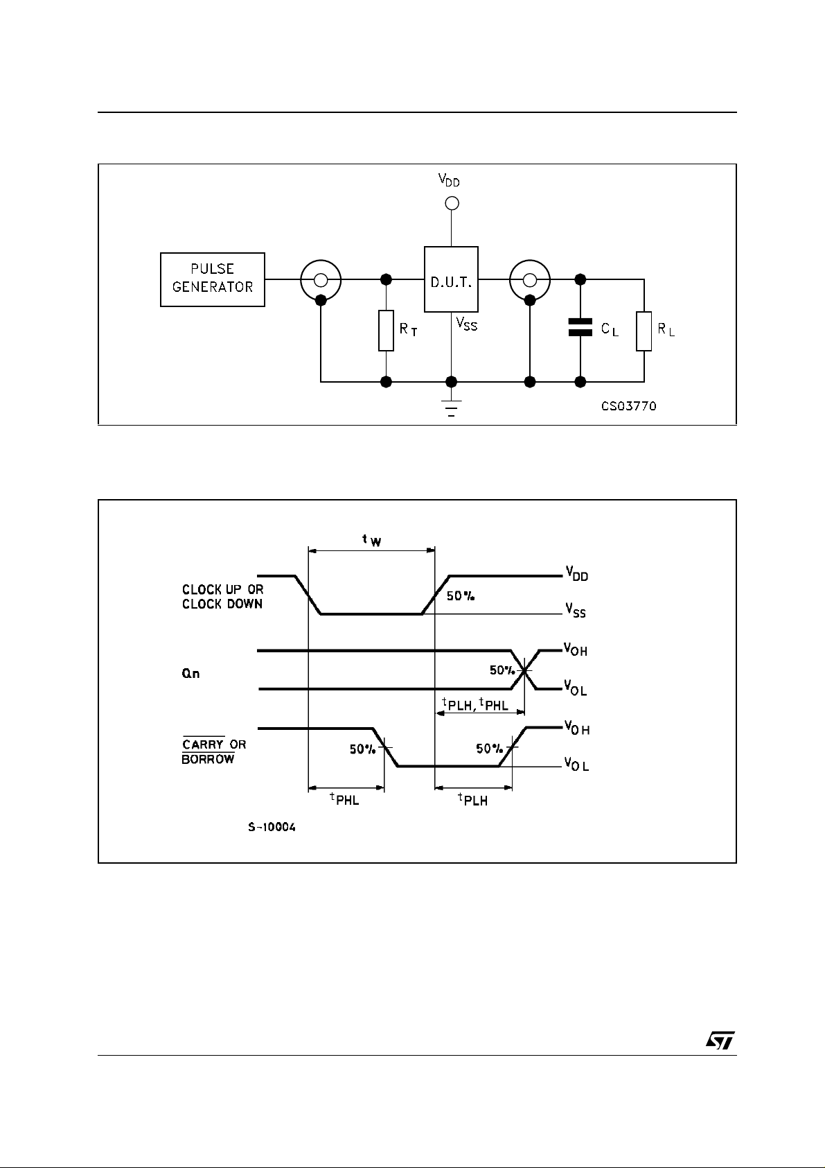
TEST CIRCUIT
CL = 50pF or equivalent (in cl udes jig and probe capac i t ance)
R
= 200K
Ω
L
R
= Z
of pulse generator (typically 50Ω)
T
OUT
WAVEFORM 1 : PROPAGATION DELAY TIMES (f=1MHz; 50% duty cycle)
8/12
Page 9
HCF40192B
WAVEFORM 2 : MINIMUM PULSE WIDTH AND REMOVAL TIME (f=1MHz; 50% duty cycle)
TYPICAL APPLICATION: CASCADED COUNTER PACKAGES
9/12
Page 10
HCF40192B
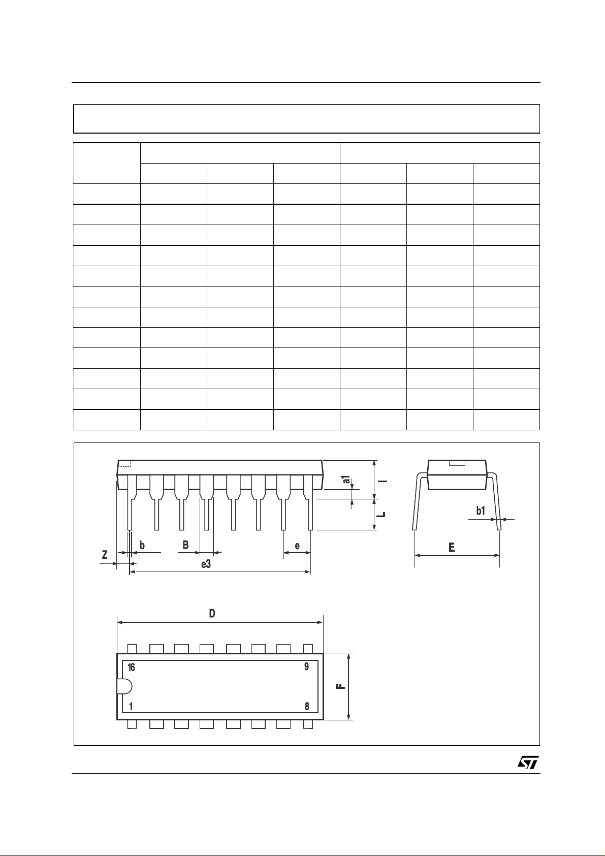
Plastic DIP-16 (0.25) MECHANICAL DATA
mm. inch
DIM.
MIN. TYP MAX. MIN. TYP. MAX.
a1 0.51 0.020
B 0.77 1.65 0.030 0.065
b 0.5 0.020
b1 0.25 0.010
D 20 0.787
E 8.5 0.335
e 2.54 0.100
e3 17.78 0.700
F 7.1 0.280
I 5.1 0.201
L 3.3 0.130
Z 1.27 0.050
10/12
P001C
Page 11
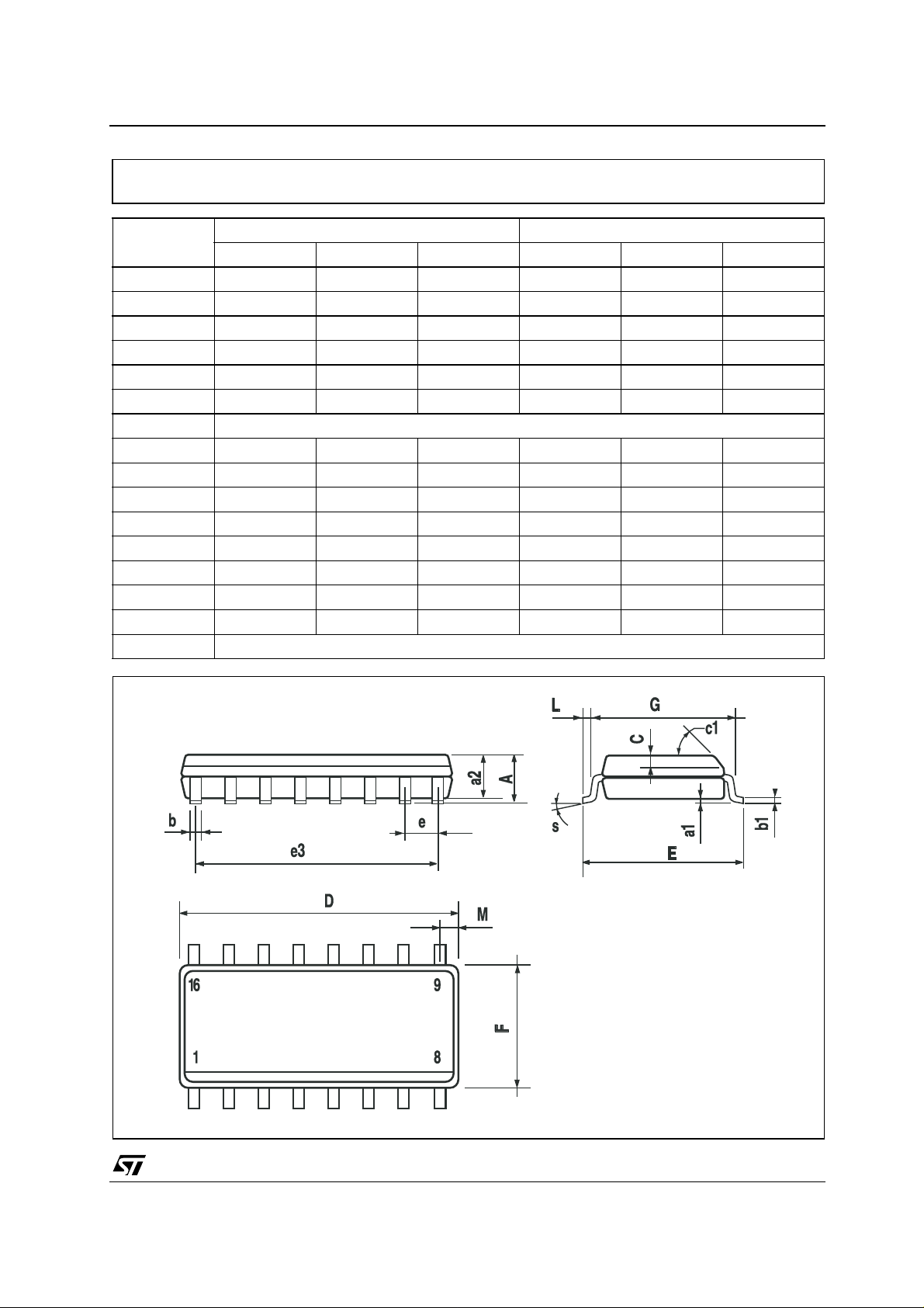
SO-16 MECHANICAL DATA
HCF40192B
DIM.
A 1.75 0.068
a1 0.1 0.2 0.003 0.007
a2 1.65 0.064
b 0.35 0.46 0.013 0.018
b1 0.19 0.25 0.007 0.010
C 0.5 0.019
c1 45˚ (typ.)
D 9.8 10 0.385 0.393
E 5.8 6.2 0.228 0.244
e 1.27 0.050
e3 8.89 0.350
F 3.8 4.0 0.149 0.157
G 4.6 5.3 0.181 0.208
L 0.5 1.27 0.019 0.050
M 0.62 0.024
S ˚ (max.)
MIN. TYP MAX. MIN. TYP. MAX.
mm. inch
8
PO13H
11/12
Page 12

HCF40192B
Information furnished is believed to be accurate and reliable. However, STMicroelectronics assumes no responsib ility for t he
consequences of use of such informatio n nor for any infringement of paten ts or o ther rig hts of t hird part ies which ma y result from
its use. No license is granted by implication or otherwise under any patent or patent rights of STMicroelectronics. Specifications
mentioned in this publication are subject to change without notice. This publication supersedes and replaces all information
previousl y suppl ied. STM icroel ectronics produc ts are not auth orized for use as c ritica l compone nts in l ife s upport dev ices or
systems without express written approval of STMicroelectronics.
Australia - Brazil - Canada - China - Finland - France - Germany - Hong Kong - India - Israel - Italy - Japan - Malaysia - Malta - Morocco
© The ST logo is a registered trademark of STMicroelectronics
© 2002 STMicroelectronics - Prin ted in Italy - All Rights Reserved
STMicroelectronics GROUP OF COMPANIES
Singapore - Spain - Sweden - Switzerland - United Kingdom - United States.
© http://www.st.com
12/12
 Loading...