

Page 1

HD61202U
(Dot Matrix Liquid Crystal GraphicDisplay Column Driver)
ADE-207-273(Z)
'99.9
Rev. 0.0
Description
HD61202U is a column (segment) driver for dot matrix liquid crystal graphic display systems. It stores the
display data transferred from a 8-bit micro controller in the internal display RAM and generates dot matrix
liquid crystal driving signals.
Each bit data of display RAM corresponds to on/off state of a dot of a liquid crystal display to provide
more flexible than character display.
As it is internally equipped with 64 output drivers for display, it is available for liquid crystal graphic
displays with many dots.
The HD61202U, which is produced in the CMOS process, can complete portable battery drive equipment
in combination with a CMOS micro-controller, utilizing the liquid crystal display’s low power dissipation.
Moreover it can facilitate dot matrix liquid crystal graphic display system configuration in combination
with the row (common) driver HD61203U.
Features
• Dot matrix liquid crystal graphic display column driver incorporating display RAM
• RAM data direct display by internal display RAM
RAM bit data 1: On
RAM bit data 0: Off
• Display RAM capacity: 512 bytes (4096 bits)
• 8-bit parallel interface
• Internal liquid crystal display driver circuit: 64
• Display duty cycle
Drives liquid crystal panels with 1/32–1/64 duty cycle multiplexing
1
Page 2

HD61202U
• Wide range of instruction function
Display data read/write, display on/off, set address, set display start line, read status
• Power supply: VCC: 2.7V~5.5V
• Liquid crystal display driving voltage: 8V to 16V
Ordering Information
Type No. Package
HD61202UFS 100-pin plastic QFP (FP-100A)
HD61202UTE 100-pin thin plastic QFP (TFP-100B)
HCD61202U Chip
2
Page 3
Pin Arrangement
(
)
HD61202U
ADC
V
V4R
V3R
V2R
V1R
V
EE2
Y64
Y63
Y62
Y61
Y60
Y59
Y58
Y57
Y56
Y55
Y54
Y53
Y52
Y51
Y50
Y49
Y48
Y47
Y46
Y45
Y44
Y43
FRMEø1ø2CL
99989796959493929190898887868584838281
100
1
2
M
3
CC
4
5
6
7
8
9
10
11
12
13
14
15
16
17
18
19
20
21
22
23
24
25
26
27
28
29
30
31323334353637383940414243444546474849
D/I
R/W
RST
CS1
HD61202UFS
(FP-100A)
CS2
CS3NCNCNCDB7
DB6
DB5
DB4
DB3
DB2
80
79
78
77
76
75
74
73
72
71
70
69
68
67
66
65
64
63
62
61
60
59
58
57
56
55
54
53
52
51
50
DB1
DB0
GND
V4L
V3L
V2L
V1L
V
EE1
Y1
Y2
Y3
Y4
Y5
Y6
Y7
Y8
Y9
Y10
Y11
Y12
Y13
Y14
Y15
Y16
Y17
Y18
Y19
Y20
Y21
Y22
Y42
Y41
Y40
Y39
Y38
Y37
Y36
Y35
Y34
Y33
Y32
Y31
Y30
Y29
Y28
Y27
Y26
Y25
Y24
Y23
Top view
3
Page 4
HD61202U
M
ADC
FRMEø1ø2CL
D/I
R/W
RSTNCCS1NCCS2
CS3NCDB7
DB6
DB5
DB4
DB3
DB2
DB1
DB0
GND
V
V4R
V3R
V2R
V1R
V
EE2
Y64
Y63
Y62
Y61
Y60
Y59
Y58
Y57
Y56
Y55
Y54
Y53
Y52
Y51
Y50
Y49
Y48
Y47
Y46
9998979695949392919089888786858483828180797877
100
1
CC
2
3
4
5
6
7
8
9
10
11
12
13
14
15
16
17
18
19
20
21
22
23
24
25
26272829303132333435363738394041424344454647484950
HD61202UTE
(TFP-100B)
76
75
74
73
72
71
70
69
68
67
66
65
64
63
62
61
60
59
58
57
56
55
54
53
52
51
V4L
V3L
V2L
Y1L
V
EE1
Y1
Y2
Y3
Y4
Y5
Y6
Y7
Y8
Y9
Y10
Y11
Y12
Y13
Y14
Y15
Y16
Y17
Y18
Y19
Y20
Y45
Y44
Y43
Y42
Y41
Y40
Y39
Y38
Y37
Y36
Y35
Y34
Y33
(Top view)
Y32
Y31
Y30
Y29
Y28
Y27
Y26
Y25
Y24
Y23
Y22
Y21
4
Page 5
HCD61202U PAD Arrangement
HD61202U
NO.3
NO.27
No.1
CHIP CODE
HD61202U
No.28
No.53
NO.78
NO.54
HCD61202U Pad Location Coordinates
PAD
No.
1
2
3
4
5
6
7
8
9
10
11
12
13
14
15
16
17
18
19
20
21
22
23
24
25
PAD
Name
XY
–1493
ADC
–1649
M
V
–1789
CC
–1789
V4R
–1789
V3R
–1789
V2R
V1R
–1789
V
–1789
EE2
–1789
Y64
–1789
Y63
–1789
Y62
–1789
Y61
–1789
Y60
Y59
–1789
–1789
Y58
–1789
Y57
Y56
–1789
Y55
–1789
Y54
–1789
Y53
–1789
Y52
–1789
–1789
Y51
Y50
–1789
Y49
–1789
–1789
Y48
Coordinate
1756
1756
1689
1445
1293
1148
1011
869
721
591
461
331
201
–60
–190
–320
–450
–580
–710
–840
–970
–1100
–1230
–1369
71
PAD
No.
26
27
28
29
30
31
32
33
34
35
36
37
38
39
40
41
42
43
44
45
46
47
48
49
50
PAD
Name
Y47
Y46
Y45
Y44
Y43
Y42
Y41
Y40
Y39
Y38
Y37
Y36
Y35
Y34
Y33
Y32
Y31
Y30
Y29
Y28
Y27
Y26
Y25
Y24
Y23
Coordinate
XY
–1789
–1789
–1764
–1604
–1452
–1312
–1171
–976
–846
–716
–586
–456
–326
–196
–65
65
195
325
455
585
715
845
975
1170
1311
–1508
–1653
–1789
–1789
–1789
–1789
–1789
–1789
–1789
–1789
–1789
–1789
–1789
–1789
–1789
–1789
–1789
–1789
–1789
–1789
–1789
–1789
–1789
–1789
–1789
Chip Size : 4.08 × 4.08 mm
Coordinate : Pad Center
Origin : Chip center
Pad Size : 90 × 90 µm
EE1
Coordinate
XY
1452
1604
1764
1789
1789
1789
1789
1789
1789
1789
1789
1789
1789
1789
1789
1789
1789
1789
1789
1789
1789
1789
1789
1789
1789
PAD
No.
51
52
53
54
55
56
57
58
59
60
61
62
63
64
65
66
67
68
69
70
71
72
73
74
75
PAD
Name
Y22
Y21
Y20
Y19
Y18
Y17
Y16
Y15
Y14
Y13
Y12
Y11
Y10
Y9
Y8
Y7
Y6
Y5
Y4
Y3
Y2
Y1
V
V1L
V2L
2
–1789
–1789
–1789
–1654
–1507
–1369
–1230
–1100
–970
–840
–710
–580
–450
–320
–190
–60
71
201
331
461
591
721
1024
1153
1293
2
PAD
No.
76
77
78
79
80
81
82
83
84
85
86
87
88
89
90
91
92
93
94
95
96
97
98
99
100
PAD
Name
V3L
V4L
GND
DB0
DB1
DB2
DB3
DB4
DB5
DB6
DB7
NC
NC
NC
CS3
CS2
CS1
RST
R/W
D/I
CL
ø2
ø1
E
FRM
Coordinate
XY
1442
1789
1789
1590
1756
1789
1756
1495
1756
1335
1756
1176
1756
1016
1756
854
1756
694
1756
535
375
1756
1756
218
1756
62
1756
–94
–249
1756
1756
–405
1756
–560
1756
–716
1756
–871
–1027
–1182
–1338
1756
1756
1756
5
Page 6
HD61202U
Block Diagram
V1L
V2L
V3L
V4L
Y1Y2Y3
Y62
Y63
Y64
V1R
V2R
V3R
V4R
ADC
V
CC
GND
V
EE1
V
EE2
1
M
1
9
XY address counter
9
Instruction
register
Liquid crystal display
2
3
driver circuit
Display data latch
2
3
4096 bit
Display data RAM
8
64 64
626364
626364
CL
6
8
6
Z address counter
line register
Display start
6
on/off
Display
FRM
Busy
flag
RST
ø1
ø2
Interface control
8
I/O buffer
3
D/I
R/W
CS1, CS2, CS3
Output registerInput register
8
8
E
DB0–DB7
6
Page 7

Terminal Functions
HD61202U
Terminal
Name
V
CC
GND
V
EE1
V
EE2
V1L, V1R
V2L, V2R
V3L, V3R
V4L, V4R
CS1
CS2
CS3
Number of
Terminals I/O Connected to Functions
2 Power supply Power supply for internal logic.
Recommended voltage is:
GND = 0V
= 2.7 to 5.5V
V
CC
2 Power supply Power supply for liquid crystal display drive circuit.
Recommended power supply voltage is V
16V. Connect the same power supply to V
V
EE1
and V
are not connected each other in the LSI.
EE2
CC–VEE
and V
EE1
= 8 to
8 Power supply Power supply for liquid crystal display drive.
Apply the voltage specified depending on liquid crystals
within the limit of V
through VCC.
EE
V1L (V1R), V2L (V2R): Selection level
V3L (V3R), V4L (V4R): Non-selection level
Power supplies connected with V1L and V1R (V2L &
V2R, V3L & V3R, V4L & V4R) should have the same
voltages.
3 I MPU Chip selection.
Data can be input or output when the terminals are in the
following conditions:
Terminal name CS1 CS2 CS3
Condition L L H
EE2
.
E 1 I MPU Enable.
At write (R/W = low): Data of DB0 to DB7 is latched at
At read (R/W = high):Data appears at DB0 to DB7 while
R/W 1 I MPU Read/write.
R/W = High: Data appears at DB0 to DB7 and can be
read by the MPU.
When E = high, CS1, CS2 = low and
CS3 = high.
R/W = Low: DB0 to DB7 can accept at fall of E when
CS1, CS2 = low and CS3 = high.
D/I 1 I MPU Data/instruction.
D/I = High: Indicates that the data of DB0 to DB7 is
display data.
D/I = Low: Indicates that the data of DB0 to DB7 is
display control data.
the fall of E.
E is at high level.
7
Page 8
HD61202U
Terminal
Name
ADC 1 I V
Number of
Terminals I/O Connected to Functions
/GND Address control signal to determine the relation between
CC
Y address of display RAM and terminals from which the
data is output.
ADC = High: Y1: H’0, Y64: H’63
ACD = Low: Y64: H’0, Y1: H’63
DB0–DB7 8 I/O MPU Data bus, three-state I/O common terminal.
M 1 I HD61203U Switch signal to convert liquid crystal drive waveform into
AC.
FRM 1 I HD61203U Display synchronous signal (frame signal).
Presets the 6-bit display line counter and synchronizes
the common signal with the frame timing when the FRM
signal becomes high.
CL 1 I HD61203U Synchronous signal to latch display data. The rising CL
signal increments the display output address counter and
latches the display data.
ø1, ø2 2 I HD61203U 2-phase clock signal for internal operation.
The ø1 and ø2 clocks are used to perform operations
(I/O of display data and execution of instructions) other
than display.
Y1–Y64 64 O Liquid crystal
display
Liquid crystal display column (segment) drive output.
The outputs at these pins are at the light-on level when
the display RAM data is 1, and at the light-off level when
the display RAM data is 0.
Relation among output level, M, and display data (D) is
as follows:
M
10
1010
V1 V3 V2 V4
RST 1 I MPU or
external CR
D
Output
level
The following registers can be initialized by setting the
RST signal to low level.
1. On/off register 0 set (display off)
2. Display start line register line 0 set (displays from line
0)
After releasing reset, this condition can be changed only
by instruction.
NC 3 Open Unused terminals. Don’t connect any lines to these
terminals.
Note: 1 corresponds to high level in positive logic.
8
Page 9
HD61202U
Function of Each Block
Interface Control
I/O Buffer: Data is transferred through 8 data bus lines (DB0–DB7).
DB7: MSB (most significant bit)
DB0: LSB (least significant bit)
Data can neither be input nor output unless CS1 to CS3 are in the active mode. Therefore, when CS1 to
CS3 are not in active mode it is useless to switch the signals of input terminals except RST and ADC; that
is namely, the internal state is maintained and no instruction excutes. Besides, pay attention to RST and
ADC which operate irrespectively of CS1 to CS3.
Register: Both input register and output register are provided to interface to an MPU whose speed is
different from that of internal operation. The selection of these registers depend on the combination of R/W
and D/I signals (Table 1).
1. Input register
The input register is used to store data temporarily before writing it into display data RAM.
The data from MPU is written into input register, then into display data RAM automatically by internal
operation. When CS1 to CS3 are in the active mode and D/I and R/W select the input register as shown
in Table 1, data is latched at the fall of the E signal.
2. Output register
The output register is used to store data temporarily that is read from display data RAM. To read out the
data from the output register, CS1 to CS3 should be in the active mode and both D/I and R/W should be
1. With the read display data instruction, data stored in the output register is output while E is high
level. Then, at the fall of E, the display data at the indicated address is latched into the output register
and the address is increased by 1.
The contents in the output register are rewritten by the read display data instruction, but are held by
address set instruction, etc.
Therefore, the data of the specified address cannot be output with the read display data instruction right
after the address is set, but can be output at the second read of data. That is to say, one dummy read is
necessary. Figure 1 shows the MPU read timing.
Table 1 Register Selection
D/I R/W Operation
1 1 Reads data out of output register as internal operation (display data RAM →
output register)
1 0 Writes data into input register as internal operation (input register → display
data RAM)
0 1 Busy check. Read of status data.
0 0 Instruction
9
Page 10
HD61202U
Busy Flag
Busy flag = 1 indicates that HD61202U is operating and no instructions except status read instruction can
be accepted. The value of the busy flag is read out on DB7 by the status read instruction. Make sure that the
busy flag is reset (0) before issuing instructions.
D/I
R/W
E
Address
Output
register
DB0–DB7
Busy
check
E
Busy
flag
Write
address N
f
CLK
N N + 1 N + 2
Busy
check
Read data
(dummy)
Figure 1 MPU Read Timing
T Busy
is ø1, ø2 frequency
Figure 2 Busy Flag
Data at address N Data at address N + 1
Busy
check
Read
data at
address N
1/f
≤ T Busy ≤ 3/f
CLK
Busy
check
CLK
Data read
address
N + 1
10
Page 11

HD61202U
Display On/Off Flip/Flop
The display on/off flip/flop selects one of two states, on state and off state of segments Y1 to Y64. In on
state, the display data corresponding to that in RAM is output to the segments. On the other hand, the
display data at all segments disappear in off state independent of the data in RAM. It is controlled by
display on/off instruction. RST signal = 0 sets the segments in off state. The status of the flip/flop is output
to DB5 by status read instruction. Display on/off instruction does not influence data in RAM. To control
display data latch by this flip/flop, CL signal (display synchronous signal) should be input correctly.
Display Start Line Register
The display start line register specifies the line in RAM which corresponds to the top line of LCD panel,
when displaying contents in display data RAM on the LCD panel. It is used for scrolling of the screen.
6-bit display start line information is written into this register by the display start line set instruction. When
high level of the FRM signal starts the display, the information in this register is transferred to the Z
address counter, which controls the display address, presetting the Z address counter.
X, Y Address Counter
A 9-bit counter which designates addresses of the internal display data RAM. X address counter (upper 3
bits) and Y address counter (lower 6 bits) should be set to each address by the respective instructions.
1. X address counter
Ordinary register with no count functions. An address is set by instruction.
2. Y address counter
An Address is set by instruction and is increased by 1 automatically by R/W operations of display data.
The Y address counter loops the values of 0 to 63 to count.
Display Data RAM
Stores dot data for display. 1-bit data of this RAM corresponds to light on (data = 1) and light off (data = 0)
of 1 dot in the display panel. The correspondence between Y addresses of RAM and segment pins can be
reversed by ADC signal.
As the ADC signal controls the Y address counter, reversing of the signal during the operation causes
malfunction and destruction of the contents of register and data of RAM. Therefore, never fail to connect
ADC pin to VCC or GND when using.
Figure 3 shows the relations between Y address of RAM and segment pins in the cases of ADC = 1 and
ADC = 0 (display start line = 0, 1/64 duty cycle).
11
Page 12

HD61202U
LCD display
pattern
Line 0
Line 1
Line 2
X = 0
Display
RAM data
Y
Y1Y2Y3Y4 Y6
1
0
0
1
0
1
0
1
1
1
0
1
0
1
0
0
00000 00000
Y5
0
1
1
0
0
0
1
0
0
0
0
1
0
0
1
0
0
1
0
0
1
1
0
1
0
0
1
0
0
0
0
0
Y
63
62
1
0
0
0
1
0
0
0
1
0
0
1
1
0
1
0
1
1
0
0
1
0
0
0
1
0
0
0
0
0
0
0
Y64
COM1
COM2
COM3
COM4
COM5
COM6
COM7
COM8
COM9
COM62
COM63
COM64
(HD61203U X1)
(HD61203U X2)
(HD61203U X3)
(HD61203U X4)
(HD61203U X5)
(HD61203U X6)
(HD61203U X7)
(HD61203U X8)
(HD61203U X9)
(HD61203U X62)
(HD61203U X63)
(HD61203U X64)
HD61202U pin name
DB0 (LSB)
DB1
DB2
DB3
DB4
DB5
DB6
DB7 (MSB)
12
Line 62
Line 63
X = 1
X = 7
1
0
0
0
1
1
1
0
0
0
01234 616263
0
1
1
0
0
0
0
5
0
0
0
1
ADC = 1 (connected to V
0
0
0
0
0
0
0
RAM Y address
)
CC
Figure 3 Relation between RAM Data and Display
Page 13

HD61202U
(
)
LCD display
pattern
Line 0
Line 1
Line 2
X = 0
Display
RAM data
Y64Y63Y62Y61Y
59 Y3Y2 Y1
1
0
0
0
0
1
0
0
1
0
0
1
1
1
1
0
0
1
0
0
1
0
0
0
00000 00000
0
1
0
0
1
0
0
1
0
0
1
1
0
1
0
0
1
0
0
0
0
0
0
1
1
1
0
0
1
0
0
0
1
0
0
1
1
0
1
0
1
1
0
0
1
0
0
0
1
0
0
0
0
0
0
0
COM1
COM2
COM3
COM4
COM5
COM6
COM7
COM8
COM9
COM62
COM63
COM64
(HD61203U X1)
(HD61203U X2)
(HD61203U X3)
(HD61203U X4)
(HD61203U X5)
(HD61203U X6)
(HD61203U X7)
(HD61203U X8)
(HD61203U X9)
(HD61203U X62)
(HD61203U X63)
(HD61203U X64)
HD61202U pin name
DB0 (LSB)
DB1
DB2
DB3
DB4
DB5
DB6
DB7 (MSB)
Line 62
Line 63
X = 1
X = 7
1
0
0
0
1
1
1
0
0
0
01234 616263
0
1
1
0
0
0
0
5
0
0
0
1
ADC = 0
0
0
0
0
0
0
0
connected to GND
Figure 3 Relation between RAM Data and Display (cont)
RAM Y address
13
Page 14

HD61202U
Z Address Counter
The Z address counter generates addresses for outputting the display data synchronized with the common
signal. This counter consists of 6 bits and counts up at the fall of the CL signal. At the high level of FRM,
the contents of the display start line register is present at the Z counter.
Display Data Latch
The display data latch stores the display data temporarily that is output from display data RAM to the liquid
crystal driving circuit. Data is latched at the rise of the CL signal. The display on/off instruction controls
the data in this latch and does not influence data in dicsplay data RAM.
Liquid Crystal Display Driver Circuit
The combination of latched display data and M signal causes one of the 4 liquid crystal driver levels, V1,
V2, V3, and V4 to be output.
Reset
The system can be initialized by setting RST terminal at low level when turning power on.
1. Display off
2. Set display start line register line 0.
While R S T is low level, no instruction except status read can be accepted. Therefore, execute other
instructions after making sure that DB4 = 0 (clear RESET) and DB7 = 0 (ready) by status read instruction.
14
Page 15

HD61202U
Display Control Instructions
Outline
Table 2 shows the instructions. Read/write (R/W) signal, data/instruction (D/I) signal, and data bus signals
(DB0 to DB7) are also called instructions because the internal operation depends on the signals from the
MPU.
These explanations are detailed in the following pages. Generally, there are following three kinds of
instructions:
1. Instruction to set addresses in the internal RAM
2. Instruction to transfer data from/to the internal RAM
3. Other instructions
In general use, the second type of instruction is used most frequently. Since Y address of the internal RAM
is increased by 1 automatically after writing (reading) data, the program can be shortened. During the
execution of an instruction, the system cannot accept instructions other than status read instruction. Send
instructions from MPU after making sure that the busy flag is 0, which is proof that an instruction is not
being executed.
15
Page 16

HD61202U
Table 2 Instructions
status are not affected. 1: on, 0: off.
screen.
access, Y address is
increased by 1.
0: Normal
0: Display on
0: Ready
RESET 1: Reset
ON/OFF 1: Display off
(X address) register.
Busy 1: Internal operation
RAM. advance. After the
to DB7 (MSB) on the address of the display
data bus into display RAM specified in
to DB7 (MSB) from the
display RAM to the data
bus.
Code
Instructions R/W D/I DB7 DB6 DB5 DB4 DB3 DB2 DB1 DB0 Functions
Display on/off 0000111111/0Controls display on/off. RAM data and internal
Display start line 0011Display start line (0–63) Specifies the RAM line displayed at the top of the
OFF
Set Y address 0001Y address (0–63) Sets the Y address in the Y address counter.
Set page (X address) 0010111Page (0–7) Sets the page (X address) of RAM at the page
Status read 1 0 Busy 0 ON/ Reset 0000Reads the status.
Write display data 0 1 Write data Writes data DB0 (LSB) Has access to the
) of ø1, and ø2.
CLK
)
CLK
≤ 3/f
BUSY
≤ T
CLK
(1/f
Read display data 1 1 Read data Reads data DB0 (LSB)
Note: Busy time varies with the frequency (f
16
Page 17

HD61202U
Detailed Explanation
Display On/Off
R/W D/I DB7 DB0
Code 000011111D
MSB LSB
The display data appears when D is 1 and disappears when D is 0. Though the data is not on the screen with
D = 0, it remains in the display data RAM. Therefore, you can make it appear by changing D = 0 into D =
1.
Display Start Line
R/W D/I DB7 DB0
Code 0011AAAAAA
MSB LSB
Z address AAAAAA (binary) of the display data RAM is set in the display start line register and displayed
at the top of the screen. Figure 4 shows examples of display (1/64 duty cycle) when the start line = 0–3.
When the display duty cycle is 1/64 or more (ex. 1/32, 1/24 etc.), the data of total line number of LCD
screen, from the line specified by display start line instruction, is displayed.
Set Page (X Address)
R/W D/I DB7 DB0
Code 0010111AAA
MSB LSB
X address AAA (binary) of the display data RAM is set in the X address register. After that, writing or
reading to or from MPU is executed in this specified page until the next page is set. See Figure 5.
Set Y Address
R/W D/I DB7 DB0
Code 0001AAAAAA
MSB LSB
Y address AAAAAA (binary) of the display data RAM is set in the Y address counter. After that, Y
address counter is increased by 1 every time the data is written or read to or from MPU.
17
Page 18

HD61202U
Status Read
R/W D/I DB7 DB0
Code 1 0 Busy 0
MSB LSB
ON/
OFF
RESET
0000
• Busy
When busy is 1, the LSI is executing internal operations. No instructions are accepted while busy is 1,
so you should make sure that busy is 0 before writing the next instruction.
• ON/OFF
Shows the liquid crystal display conditions: on condition or off condition.
When on/off is 1, the display is in off condition.
When on/off is 0, the display is in on condition.
• RESET
RESET = 1 shows that the system is being initialized. In this condition, no instructions except status
read can be accepted.
RESET = 0 shows that initializing has finished and the system is in the usual operation condition.
18
Page 19

HD61202U
COM1
COM2
COM3
COM4
COM5
COM6
COM7
COM8
COM9
COM60
COM61
COM62
COM63
COM64
COM1
COM2
COM3
COM4
COM5
COM6
COM7
COM8
COM9
Start line = 0
COM1
COM2
COM3
COM4
COM5
COM6
COM7
COM8
COM9
COM60
COM61
COM62
COM63
COM64
Start line = 1
COM1
COM2
COM3
COM4
COM5
COM6
COM7
COM8
COM9
COM60
COM61
COM62
COM63
COM64
COM60
COM61
COM62
COM63
COM64
Start line = 2
Figure 4 Relation between Start Line and Display
Start line = 3
19
Page 20

HD61202U
Write Display Data
R/W D/I DB7 DB0
Code 0 1DD DDDD
MSB LSB
Writes 8-bit data DDDDDDDD (binary) into the display data RAM. Then Y address is increased by 1
automatically.
Read Display Data
R/W D/I DB7 DB0
Code 1 1DD DDDD
MSB LSB
Reads out 8-bit data DDDDDDDD (binary) from the display data RAM. Then Y address is increased by 1
automatically.
One dummy read is necessary right after the address setting. For details, refer to the explanation of output
register in “Function of Each Block”.
DD
DD
Y address
012 616263
DB0
to
Page 0
X = 0
DB7
DB0
to
Page 1
X = 1
DB7
DB0
to
Page 6
X = 6
DB7
DB0
to
Page 7
X = 7
DB7
Figure 5 Address Configuration of Display Data RAM
20
Page 21

Use of HD61202U
Interface with HD61203 (1/64 Duty Cycle)
RfC
f
RCRC
HD61202U
V
CC
V1
V6
V5
V2
V
EE
V
CC
Power supply circuit
+5V (VCC)
R1
R1
R2
R1
–
+
–
+
–
+
–
+
R1
–10V
Contrast
V
V1L, V1R
V6L, V6R
V5L, V5R
V2L, V2R
V
GND
SHL
DS1
DS2
TH
CL1
FS
M/S
FCS
STB
R3 V1
R3 V6
R3
V3
R3
V4
R3 V5
R3 V2
V
EE
CC
EE
HD61203U
R3 = 15 Ω
X1
X64
DL
DR
M
CL2
FRM
ø1
ø2
V
CC
External CR
Open
Open
M
CL
FRM
ø1
ø2
ADC
RST
CS1
CS2
CS3
COM1
COM64
HD61202U
R/W
D/IEDB0
LCD panel
64 × 64 dots
SEG1
Y1 Y64
V1L, V1R
V2L, V2R
V3L, V3R
V4L, V4R
V
, V
EE1
DB1
DB2
DB3
DB4
DB5
DB6
MPU
SEG64
V
CC
EE2
GND
DB7
V
V1
V2
V3
V4
V
CC
EE
21
Page 22

HD61202U
ø1
Input
COM
ø2
CL
FRM
M
X1
X2
X64
123 4849
64 1 2 3 64 1 2 3
1 frame
1 frame
V1
V6
V5
V5
V5
V1
V2
V6
V6
V5
V2
V6
V2
V5
V1
V5
V5
64
1
V2
V6
V1
V6
V1
V3
V4
Y1
SEG
V4
Y64
The waveforms of Y1 to Y64 outputs vary with the display data. In this example, the top line of
the panel lights up and other dots do not.
V1
Selected
V3
Non-selected
V2
V2
V4
V4
V1
V1
Figure 6 LCD Driver Timing Chart (1/64 Duty Cycle)
22
Page 23

Interface with CPU
1. Example of Connection with H8/536S
A15
to
A1
AS
Decoder
HD61202U
CS1
CC
CS2
CS3
V
H8/536S
A
R/W
E
D0
to
D7
RES
V
CC
Figure 7 Example of Connection with H8/536S
D/I
R/W
HD61202U
E
DB0
to
DB7
RST
23
Page 24

HD61202U
Example of Application
In this example, two HD61203s output the equivalent waveforms. So, stand-alone operation is possible. In
this case, connect COM1 and COM65 to X1, COM2 and COM66 to X2, ..., and COM64 and COM128 to
X64. However, for the large screen display, it is better to drive in 2 rows as in this example to guarantee the
display quality.
X1
X2
X3
(master)
HD61203U
X64
X1
X2
X3
(slave)
HD61203U
X64
COM1
COM2
COM3
COM64
COM65
COM66
COM67
COM128
HD61202U
No. 9
Y1 Y64
HD61202U
No. 10
Y1 Y64
LCD panel
128 × 480 dots
HD61202U
No. 16
Y1 Y32
24
Y1 Y64
HD61202U
No. 1
Y1 Y64
HD61202U
No. 2
Figure 8 Application Example
Y1 Y32
HD61202U
No. 8
Page 25

HD61202U
Absolute Maximum Ratings
Item Symbol Value Unit Note
Supply voltage V
CC
V
EE1
V
EE2
Terminal voltage (1) VT1 VEE – 0.3 to VCC + 0.3 V 4
Terminal voltage (2) VT2 –0.3 to V
Operating temperature T
Storage temperature T
opr
stg
Notes: 1. LSIs may be destroyed if they are used beyond the absolute maximum ratings.
In ordinary operation, it is desirable to use them within the recommended operation conditions.
Useing them beyond these conditions may cause malfunction and poor reliability.
2. All voltage values are referenced to GND = 0V.
3. Apply the same supply voltage to V
4. Applies to V1L, V2L, V3L, V4L, V1R, V2R, V3R, and V4R.
Maintain
V
≥ V1L = V1R ≥ V3L = V3R ≥ V4L = V4R ≥ V2L = V2R ≥ V
CC
5. Applies to M, FRM, CL, RST, ADC, ø1, ø2, CS1, CS2, CS3, E, R/W, D/I, and DB0–DB7.
–0.3 to +7.0 V 2
V
– 17.0 to VCC + 0.3 V 3
CC
+ 0.3 V 2, 5
CC
–30 to +75 °C
–55 to +125 °C
EE1
and V
EE2
.
EE
25
Page 26

HD61202U
Electrical Characteristics (GND = 0V, V
Ta = −30 ~ +75°C)
*8
= 2.7 ~ 5.5V, VCC − VEE = 8.0 to 16.0V,
CC
Limit
Item Symbol Min Typ Max Unit Test Condition Notes
Input high voltage VIHC 0.7V
VIHT 0.7V
CC
CC
2.0 — V
Input low voltage VILC 0.0 0.3V
—V
—V
CC
CC
CC
CC
VVCC = 2.7V~5.5V 1
VVCC = 2.7V~4.5V 2
VVCC = 4.5V~5.5V 2
VV
= 2.7V~5.5V 1
CC
VILT 0.0 — 0.5 V VCC = 2.7V~4.5V 2
0.0 0.8 V VCC = 4.5V~5.5V 2
Output high voltage VOH 0.75V
2.4 — — V IOH = –205 µA
Output low voltage VOL — 0.2V
— — 0.4 V IOL = 1.2mA,
Input leakage current I
Three-state (off)
input current
Liquid crystal supply
leakage current
Driver on resistance R
Dissipation current I
IL
I
TSL
I
LSL
ON
CC
I
CC
–1 — 1 µA Vin = GND ~ V
–5 — 5 µA Vin = GND ~ V
–2 — 2 µA Vin = VEE–V
— — 7.5 kΩ±I
(1) — — 100 µA During display 7
(2) — — 500 µA During access,
—— V IOH = –100 µA,
CC
CC
VIOL = 100 uA,
V
= 2.7V~4.5V
CC
V
= 4.5V~5.5V
CC
V
= 2.7V~4.5V
CC
V
= 4.5V~5.5V
CC
CC
= 0.1 mA,
LOAD
V
= 15V
CC–VEE
Cycle = 1MHz
3
3
3
3
CC
CC
4
5
6
8
7
Notes: 1. Applies to M, FRM, CL, RST, ø1, and ø2.
2. Applies to CS1, CS2, CS3, E, R/W, D/I, and DB0–DB7.
3. Applies to DB0–DB7.
4. Applies to terminals except for DB0–DB7.
5. Applies to DB0–DB7 at high impedance.
6. Applies to V1L–V4L and V1R–V4R.
7. Specified when LCD is in 1/64 duty cycle mode.
Operation frequency:f
Frame frequency: f
= 250 kHz (ø1 and ø2 frequency)
CLK
= 70 Hz (FRM frequency)
M
Specified in the state of
Output terminal: Not loaded
Input level: VIH = V
(V)
CC
VIL = GND (V)
Measured at V
terminal
CC
8. Specified at +75°C for die products.
26
Page 27

HD61202U
9. Resistance between terminal Y and terminal V (one of V1L, V1R, V2L, V2R, V3L, V3R, V4L, and
V4R) when load current flows through one of the terminals Y1 to Y64. This value is specified
under the following condition:
VCC–VEE = 15.0V
V1L = V1R, V3L = V3R = V
V2L = V2R, V4L = V4R = V
V1L, V1R
–2/7 (VCC–VEE)
CC
+2/7 (VCC–VEE)
CC
RON
V3L, V3R
V4L, V4R
Terminal Y
(Y1–Y64)
V2L, V2R
The following is a description of the range of power supply voltage for liquid crystal display drive.
Apply positive voltage to V1L = V1R and V3L = V3R and negative voltage to V2L = V2R and V4L
= V4R within the ∆V range. This range allows stable impedance on driver output (RON). Notice
that ∆V depends on power supply voltage V
V
V1 (V1L = V1R)
∆V
V3 (V3L = V3R)
CC
CC–VEE
.
Range of power supply
voltage for liquid crystal
display drive
5.0
∆V (V)
3
∆V
V4 (V4L = V4R)
V2 (V2L = V2R)
V
EE
Correlation between driver output
waveform and power supply voltages
Correlation between power supply
voltage V
816
V
CC–VEE
CC–VEE
(V)
and ∆V
for liquid crystal display drive
27
Page 28

HD61202U
Terminal Configuration
Input Terminal
Input/Output Terminal
V
CC
PMOS
NMOS
V
CC
(Input circuit)
PMOS
NMOS
Applicable terminals:
M, FRM, CL, RST, ø1, ø2, CS1, CS2, CS3,
E, R/W, D/I, ADC
Applicable terminals: DB0–DB7
V
CC
Enable
PMOS
Data
NMOS
Output Terminal
28
(Output circuit)
[three state]
Applicable terminals:
PMOS
V
CC
PMOS
V
CC
NMOS
V
EE
NMOS
V
EE
V1L, V1R
V3L, V3R
V4L, V4R
V2L, V2R
Y1–Y64
Page 29

Interface AC Characteristics
HD61202U
MPU Interface (GND = 0V, VCC = 2.7 to 5.5V, Ta = –30 to +75°C)
*
Item Symbol Min Typ Max Unit Note
E cycle time t
E high level width P
E low level width P
E rise time t
E fall time t
Address setup time t
Address hold time t
Data setup time t
Data delay time t
Data hold time (write) t
Data hold time (read) t
CYC
WEH
WEL
r
f
AS
AH
DSW
DDR
DHW
DHR
1000 — — ns Fig. 10, Fig. 11
450 — — ns
450 — — ns
— — 25 ns
— — 25 ns
140 — — ns
10 — — ns
200 — — ns Fig. 10
— — 320 ns Fig. 11, Fig. 12
10 — — ns Fig. 10
20 — — ns Fig. 11
Note: Specified at +75°C for die products.
t
CYC
VIHT
VILT
VIHT
VILT
P
WEL
P
WEH
t
t
DSW
f
t
AH
t
AH
t
DHW
t
r
t
AS
t
AS
VIHT
VILT
E
VIHT
R/W
CS1–CS3
D/I
DB0–DB7
VILT
Figure 9 MPU Write Timing
29
Page 30

HD61202U
t
CYC
E
R/W
CS1–CS3
D/I
DB0–DB7
VIHT
VILT
VIHT
VILT
P
WEL
t
AS
t
AS
P
WEH
t
r
t
DDR
t
f
t
AH
t
AH
VIHT
VILT
Figure 10 MPU Read Timing
VCC = 4.5V to 5.5V VCC = 2.7V to 4.5V
Test point
11kΩ90pF
D1
V
CC
= 5V
2.4kΩ
Test point
Diodes
IS2074 H
t
DHR
50pF
Notes) including jip capacitance
Figure 11 DB0–DB7: Load Circuit
30
Page 31

HD61202U
Clock Timing (GND = 0V, VCC = 2.7 to 5.5V, Ta = –30 to +75°C)
*
Limit
Item Symbol Min Typ Max Unit Test Condition
ø1, ø2 cycle time t
ø1 low level width t
ø2 low level width t
ø1 high level width t
ø2 high level width t
ø1–ø2 phase difference t
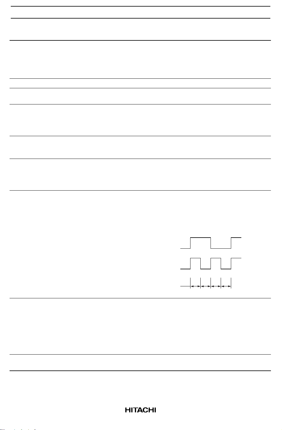
ø2–ø1 phase difference t
ø1, ø2 rise time t
ø1, ø2 fall time t
cyc
WLø1
WLø2
WHø1
WHø2
D12
D21
r
f
2.5 — 20 µs Fig. 13
625 — — ns
625 — — ns
1875 — — ns
1875 — — ns
625 — — ns
625 — — ns
— — 150 ns
— — 150 ns
Note: Specified at +75°C for die products.
t
cyc
t
f
t
r
t
WHø1
ø1
ø2
VIHC
VILC
t
WLø1
t
D12
VIHC
VILC
t
f
t
WLø2
t
D21
t
t
r
t
cyc
Figure 12 External Clock Waveform
WHø2
31
Page 32

HD61202U
Display Control Timing (GND = 0V, VCC = 2.7 to 5.5V, Ta = –30 to +75°C)
*
Limit
Item Symbol Min Typ Max Unit Test Condition
FRM delay time t
M delay time t
CL low level width t
CL high level width t
DFRM
DM
WLCL
WHCL
–2 — +2 µs Fig. 14
–2 — +2 µs
35 — — µs
35 — — µs
Note: Specified at +75°C for die products.
t
WLCL
t
WHCL
t
DFRM
CL
VIHC
VILC
t
DFRM
VIHC
FRM
VILC
t
DM
M
VILC
Figure 13 Display Control Signal Waveform
VIHC
Reset Timing (GND = 0V, VCC = 2.7 to 5.5V, Ta = –30 to +75°C)
Item Symbol Min Typ Max Unit
Reset time t
RST
Do not fail to set the system again because RESET during operation may destroy the data in all the registers
except on/off register and in RAM.
RST VILC
1.0 — — µs
t
RST
Reset timing
*
Figure 14 Reset Timing
32
Page 33

HD61202U
Cautions
1. Hitachi neither warrants nor grants licenses of any rights of Hitachi’s or any third party’s patent,
copyright, trademark, or other intellectual property rights for information contained in this document.
Hitachi bears no responsibility for problems that may arise with third party’s rights, including
intellectual property rights, in connection with use of the information contained in this document.
2. Products and product specifications may be subject to change without notice. Confirm that you have
received the latest product standards or specifications before final design, purchase or use.
3. Hitachi makes every attempt to ensure that its products are of high quality and reliability. However,
contact Hitachi’s sales office before using the product in an application that demands especially high
quality and reliability or where its failure or malfunction may directly threaten human life or cause risk
of bodily injury, such as aerospace, aeronautics, nuclear power, combustion control, transportation,
traffic, safety equipment or medical equipment for life support.
4. Design your application so that the product is used within the ranges guaranteed by Hitachi particularly
for maximum rating, operating supply voltage range, heat radiation characteristics, installation
conditions and other characteristics. Hitachi bears no responsibility for failure or damage when used
beyond the guaranteed ranges. Even within the guaranteed ranges, consider normally foreseeable
failure rates or failure modes in semiconductor devices and employ systemic measures such as failsafes, so that the equipment incorporating Hitachi product does not cause bodily injury, fire or other
consequential damage due to operation of the Hitachi product.
5. This product is not designed to be radiation resistant.
6. No one is permitted to reproduce or duplicate, in any form, the whole or part of this document without
written approval from Hitachi.
7. Contact Hitachi’s sales office for any questions regarding this document or Hitachi semiconductor
products.
Hitachi, Ltd.
Semiconductor & Integrated Circuits.
Nippon Bldg., 2-6-2, Ohte-machi, Chiyoda-ku, Tokyo 100-0004, Japan
Tel: Tokyo (03) 3270-2111 Fax: (03) 3270-5109
URL NorthAmerica : http:semiconductor.hitachi.com/
For further information write to:
Hitachi Semiconductor
(America) Inc.
179 East Tasman Drive,
San Jose,CA 95134
Tel: <1> (408) 433-1990
Fax: <1>(408) 433-0223
Europe : http://www.hitachi-eu.com/hel/ecg
Asia (Singapore) : http://www.has.hitachi.com.sg/grp3/sicd/index.htm
Asia (Taiwan) : http://www.hitachi.com.tw/E/Product/SICD_Frame.htm
Asia (HongKong) : http://www.hitachi.com.hk/eng/bo/grp3/index.htm
Japan : http://www.hitachi.co.jp/Sicd/indx.htm
Hitachi Europe GmbH
Electronic components Group
Dornacher Straße 3
D-85622 Feldkirchen, Munich
Germany
Tel: <49> (89) 9 9180-0
Fax: <49> (89) 9 29 30 00
Hitachi Europe Ltd.
Electronic Components Group.
Whitebrook Park
Lower Cookham Road
Maidenhead
Berkshire SL6 8YA, United Kingdom
Tel: <44> (1628) 585000
Fax: <44> (1628) 778322
Hitachi Asia Pte. Ltd.
16 Collyer Quay #20-00
Hitachi Tower
Singapore 049318
Tel: 535-2100
Fax: 535-1533
Hitachi Asia Ltd.
Taipei Branch Office
3F, Hung Kuo Building. No.167,
Tun-Hwa North Road, Taipei (105)
Tel: <886> (2) 2718-3666
Fax: <886> (2) 2718-8180
Copyright © Hitachi, Ltd., 1998. All rights reserved. Printed in Japan.
Hitachi Asia (Hong Kong) Ltd.
Group III (Electronic Components)
7/F., North Tower, World Finance Centre,
Harbour City, Canton Road, Tsim Sha Tsui,
Kowloon, Hong Kong
Tel: <852> (2) 735 9218
Fax: <852> (2) 730 0281
Telex: 40815 HITEC HX
33
 Loading...