

Page 1
[ /Title
(HC60
94)
/Subject
(ADSL
Analog
Front
End
Chip)
/Autho
r ()
/Keywords
(Harris
Semiconductor,
Telecom,
SLICs,
SLACs
, Telephone,
Telephony,
WLL,
Wireless
Local
Loop,
PBX,
Private
Branch
Exchan
ge,
NT1+,
CO,
Cen-
Semiconductor
NO RECOMMENDED REPLACEMENT
February 1999
Call Central Applications 1-800-442-7747
or email: centapp@harris.com
Features
• 14-Bit 5 MSPS DAC
• Programmable Gain Stages
• Anti-Aliasing and Reconstruction Filters
Applications
• FDM DMT ADSL
• CAP ADSL
• EC DMT ADSL
• Communications Receiver
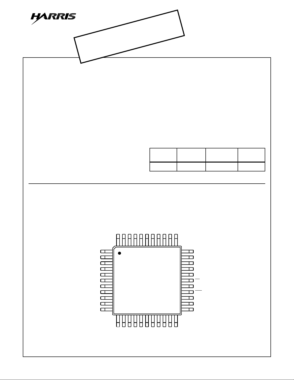
Pinout
D11
D10
D9
D8
D7
D6
D5
D4
D3
D2
D1
OBSOLETE PRODUCT
Description
The HC6094 performs the Analog processing for the ADSL
chip set. The transmit chain has a 14 Bit DAC, a third-order
Chebyshev reconstruction filter and a programmable attenuator (-12 to 0dB) capable of driving a 220Ω differential load.
The receiver chain has a high impedance input stage, programmable gain stage (0 to 24dB), additional programmable
gain (-9 to 18dB) and a third-order Chebyshev anti-aliasing
filter for driving an off-chip A/D.
Laser trimmable thin-film resistors are used to set the filter
cutoff frequency and DAC linearity. The transmit and receive
signal chains are specified at 65dB MTPR.
Ordering Information
HC6094
(MQFP)
TOP VIEW
D12
D13 (MSB)
VDDD_TX
CLK
GNDD_TX
CTLIN
44 43 42 41 40
1
2
3
4
5
6
7
8
9
10
11
12 13 14 15 16 17
RXO-
RXO+
D0 (LSB)
39 38 37 36 35 34
PGAI-
VSSA_RX
VDDA_RX
HC6094
ADSL Analog Front End Chip
PART
NUMBER
HC6094IN -40 to 85 44 Ld MQFP Q44.10x10
CTLOUT
GNDA_TX
VDDA_ATT
PGAI+
PGAO-
PGAO+
TEMP.
RANGE (oC) PACKAGE PKG. NO.
TXO-
TXO+
VSSA_ATT
VDDA_TX
VSSA_TX
ARTN
VDDD_RX
CS
SDI
RST
SCLK
GNDD__RX
GNDA_RX
2221201918
RXI+
33
32
31
30
29
28
27
26
25
24
23
RXI-
CAUTION: These devices are sensitive to electrostatic discharge. Users should follow proper IC Handling Procedures.
Copyright
© Harris Corporation 1999
1
File Number 4260.2
Page 2
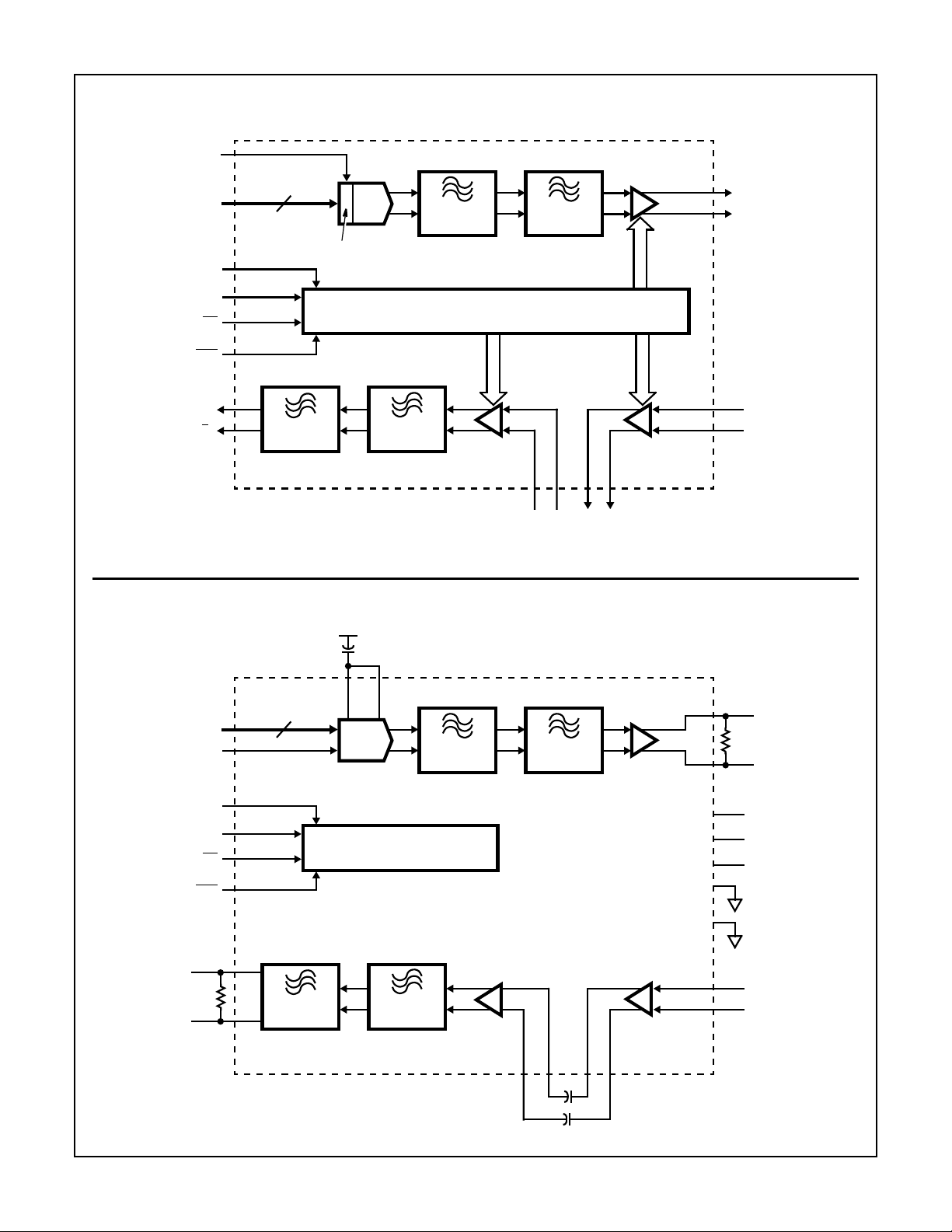
Functional Block Diagram
HC6094
CLK
D0-D13
SCLK
SDI
CS
RST
+
RXO
Typical Setup
14
2ND ORDER
1.1MHz LPF
DAC
LATCH
RECEIVER
TRANSMITTER
1ST ORDER
1.1MHz LPF
SHIFT REGISTER AND LATCHES
1ST ORDER
1.1MHz LPF
PGA2
-9 TO 18dB 0 TO 24dB
2ND ORDER
1.1MHz LPF
PGAO±PGAI±
-12 TO 0dB
PGA0
TX O±
RXI±
PGA1
RXO±
D0-D13
CLK
SCLK
SDI
CS
RST
+
-
RL = 2000
VSSA_TX
CTLIN CTLOUT
14
DAC
SHIFT REGISTER AND LATCHES
2ND ORDER
1.1MHz LPF
1ST ORDER
1.1MHz LPF
RECEIVER
1ST ORDER
1.1MHz LPF
-9 TO 18dB 0 TO 24dB
PGA2
2ND ORDER
1.1MHz LPF
-12 TO 0dB
PGA0
VDDD_TX, RX
VDDA_TX, RX
VSSA_TX, RX
GNDD_TX, RX
GNDA_RX, TX
PGA1
PGA OUTPGA IN
+
TX O±
-
= 220
R
L
+5V
+5V
-5V
RXI±
2
Page 3
HC6094
Absolute Maximum Ratings T
Supply Pins . . . . . . . . . . . . . . . . . . . . . . . . . . . . . . . . . . . . . . . . . . . .±5.5V
Analog Input Voltage to Ground. . . . . . . . . . . .VDD+0.5, VSS -0.5V
Digital Input Voltage to Ground. . . . . . . . . . . . . . . .VDD+0.5V, -0.5V
=25oC Thermal Information
A
Thermal Resistance (Typical, Note 1) θJA (oC/W)
MQFP . . . . . . . . . . . . . . . . . . . . . . . . . . . . . . . . . . . 55
Maximum Pow er Dissipation. . . . . . . . . . . . . . . . . . . . . . . . . . . . . 1.18W
Maximum Junction Temperature (TJ) . . . . . . . . . . . . . . . . . . . . 150oC
Operating Conditions
Temperature Range . . . . . . . . . . . . . . . . . . . . . . . . . . -40oC to 85oC
CAUTION: Stresses above those listed in “Absolute Maximum Ratings” may cause permanent damage to the device. This is a stress only rating and operation
of the device at these or any other conditions above those indicated in the operational sections of this specification is not implied.
Maximum Storage Temperature Range . . . . . . . . . .-65oC to 150oC
Maximum Lead Temperature (Soldering 10s). . . . . . . . . . . . . 300oC
(Lead Tips Only)
NOTE:
1. θJA is measured with the component mounted on an evaluation PC board in free air.
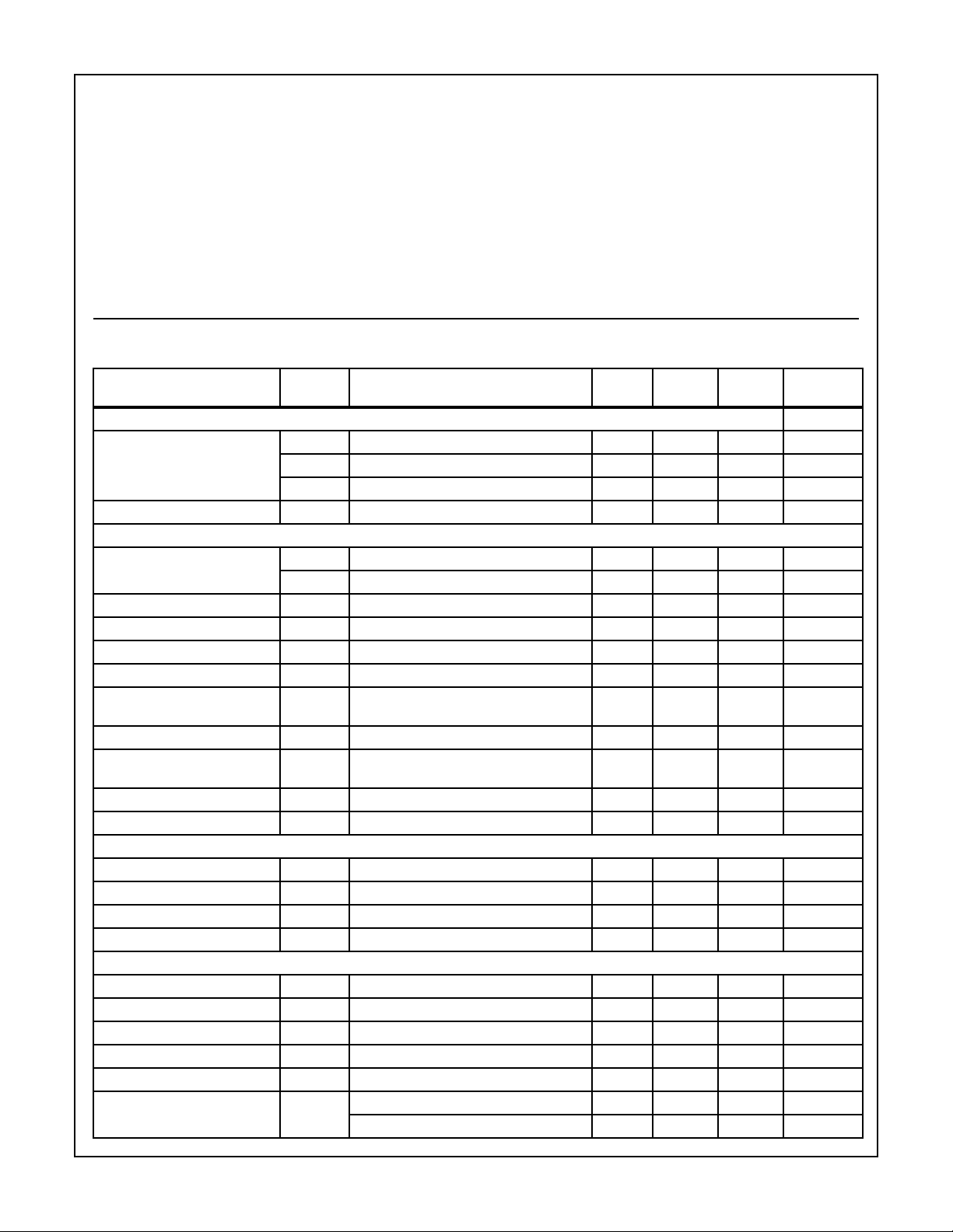
Electrical Specifications V
=5V,VSS= -5V, RLOpen, Over Temperature Range; Unless Otherwise Specified. Designed for ±5%
DD
Power Supply.
TEST
PARAMETER SYMBOL
CONDITIONS MIN TYP MAX UNITS
OVERALL
Supply Currents I
I
I
VDD (Note 2) - 66 - mA
DD
VSS (Note 3) - -79 - mA
SS
CC
V
CC
-0- µA
Power Dissipation PD Quiescent, No Load - 725 - mW
DIGITAL INTERFACE
Input Voltage Thresholds V
Input Currents I
IL
V
IH
VIN = 0V -10.0 0 10.0 µA
IL
I
VIN = V
IH
DD
- - 0.8 V
2.7 - - V
-10.0 0 10.0 µA
Serial Clock Period T1 0.1 - 5.0 µs
CS Active Before Shift Edge T2 T1/2 -10 - - ns
Write Data Valid After Shift
T3 - - 10 ns
Edge
CS Inactive After Latch Edge T4 T1 - 10 - T1 +10 ns
Write Data Hold After Latch
T5 T1/2 -5 - T1/2 +5 ns
Edge
DAC Setup Time t
DAC Hold Time t
S
H
- - 100 ns
- - 100 ns
14-BIT DAC
Resolution/Monotonicity 14 - - Bits
Integral Linearity I
Differential Linearity D
Measured at TX Outputs - ±1.5 - LSB
LE
LE
- ±0.9 - LSB
Max Sample Rate 4.416 - - Ms/s
TRANSMITTER OUTPUT
Output Drive TXOD Sink or Source 30 55 - mA
Differential Output Swing TXOS RL= 220Ω 11.7 12.03 12.3 V
PP
Differential Balance TXDB Gain Match Between Outputs - 0.5 - %
Transmit Output Offset TXOFF Max Gain Single Ended (Note 4) -200 25 200 mV
Multi-Tone Power Ratio TXMTPR RL= 220Ω -65- dB
Power Supply Rejection PSRR Input Referred - V
Input Referred - V
DD
SS
40 65 - dB
55 84 - dB
3
Page 4

HC6094
Electrical Specifications V
=5V,VSS= -5V, RLOpen, Over Temperature Range; Unless Otherwise Specified. Designed for ±5%
DD
Power Supply. (Continued)
TEST
PARAMETER SYMBOL
CONDITIONS MIN TYP MAX UNITS
TRANSMITTER GAIN STAGE
Gain Error TXPG RL= 220Ω, 0dB Setting -0.22 +0.02 0.22 dB
RL= 220Ω, Each Step Relative to 0dB -0.15 0.02 0.15 dB
TRANSMITTER FREQUENCY RESPONSE
Gain Ripple Peak to Peak GP Across 1.104MHz Bandwidth - 0.2 0.6 dB
Stopband Attenuation GS At 2.65MHz 14 17 - dB
Floor Attenuation GM At 9.94MHz - 58 - dB
RECEIVER INPUT (PGA1 AND PGA2)
Input Swing RXIS Differential - - 12 V
PP
Input Impedance RXRIN PGA1 1.0 - MΩ
PGA2 1.0 12 - kΩ
Common Mode Rejection RXCMRR 1.1MHz - 90 - dB
Common Mode Range RXCMIR -0.25 - 0.25 V
Continuous Input Voltage VSS-0.5 VDD +0.5 V
RECEIVER OUTPUT (INCLUDING PGA1 OUT)
Differential Output Swing RXOS RX
Differential Balance RXDB End to End (RXIN to RX
(RL = 2000Ω) 12.0 15.8 - V
OUT
PGA1
(RL = 2000Ω) 12.0 16.0 - V
OUT
) - 0.5 - %
OUT
PP
PP
PGA1 Output Offset RXOFF Max Gain Single Ended (Note 4) -200 40 200 mV
PGA2 Output Offset RXOFF Max Gain Single Ended (Note 4) -200 30 200 mV
Multi-Tone Power Ratio RXMTPR RL = 2000Ω -65- dB
Power Supply Rejection PSRR Input Referred - V
Input Referred - V
DD
SS
45 69 - dB
55 84 - dB
RECEIVER GAIN STAGE
Absolute Gain Error RXPG Any Step (RXIN to RX
) -0.3 0.01 0.3 dB
OUT
RECEIVER FREQUENCY RESPONSE
Gain Ripple Peak to Peak GP Across 1.104MHz Bandwidth - 0.4 0.6 dB
Stopband Attenuation GS At 2.65MHz 14 19.4 - dB
Floor Attenuation GM At 9.94MHz - 53 - dB
TRANSMITTER AND RECEIVER FILTER CUTOFF FREQUENCY
TX Filter F
RX Filter F
C
C
TX
RX
-0.15dB point 1.104 1.18 1.25 MHz
FC
-0.15dB point 1.104 1.125 1.16 MHz
FC
NOTES:
2. VDD = 5V typical, supply range ±5%.
3. VSS = -5V typical, supply range ±5%.
4. Single ended operation for reference only. Probed to these limits, but not packaged tested.
4
Page 5

HC6094
Definitions
1. Supply currents/power dissipation measured in a quiescent (static) state with RL open.
2. Logic input levels and timing are verified by using them as conditions for testing DAC and filter.
3. Digital input currents are measured at 0V and V
4. DAC resolution and monotonicity guaranteed by ILE and DLE tests.
5. DAC ILE is relative to best fit straight line.
6. Output drive current is the output current at 0V for each output when they are driven to ± Full Scale.
7. Output offset measured with V
= 0V differential for the RX, and the DAC at mid scale for the TX.
IN
8. PSRR is the change in differential input voltage vs. change in supply voltage at DC.
Gain is calculated as 20*Log((TXout
9. T
X
input swing is verified by using this as condition for gain testing.
10. R
X
Input Impedance is calculated as ∆VIN/∆IIN where VIN is the maximum input voltages, with the PGA set to 0dB.
11. R
X
12. RXCMRR is calculated as 20*Log(V
DACFS
OUT/VIN
set to maximum.
.
CC
- TXout
DACZS
)/12V) at DC.
)-PGA Gain. VINis set to 250mV
(CMIR) at 1.1MHz, and PGA gain is
PEAK
13. R
Gain is calculated as 20*Log(dV
X
/dVIN), where VINis set to give a nominal ± Output Swing, or the maximum input
OUT
swing, whichever is smaller. It is tested DC.
14. Filter Gain/Attenuation is relative to low frequency passband gain. T
R
tested by driving PGA2. Wafer probe will use special test points to bypass the DAC for laser trimming.
X
tested by driving the DAC (with sinX/X correction),
X
15. MTPR -(Multi-Tone Power Ratio). A DMT waveform is generated which has a specific crest factoror peak to average ratio
(PAR) with specific carriers missing. The waveformis then passed through the T
or RXchain. The total integrated power
X
of the notch at the location of the missing carriers is measured with respect to the adjacent carriers. Notch depth is measured for severalDMT waveforms with different PARs. The notch depths for each DMT waveform are averaged to give an
MTPR number.
5
Page 6

Shift Register Format
HC6094
Each write operation to a control register involves 16 bits of
data. The CS- signal must be enabled low during any serial
write operation. The data on SDI shall be clocked in during
CS-
SCLK
SDI
FIGURE 1. SERIAL CONTROL
Logic Timing Definitions
CS
SCLK
the rising edge of SCLK. A3-A0 supply the address of the
control register, and D7-D0 supply the data.
0000 A0A1A2A3 D0D1D2D3D4D5D6D7
SCLK
SDI
DAC DATA
CLK
t
2
t
t
3
5
t
1
FIGURE 2. SERIAL INTERFACE
tSt
H
FIGURE 3. DAC INTERFACE
t
4
6
Page 7

HC6094
Shift Registers Format
REGISTER A0 A1 A2 A3 D0 D1 D2 D3 D4 D5 D6 D7
RX Gain 1 0 X X PGA1 Gain PGA2 Gain
TX Gain 0 0 X X PGA0 Gain
TX PGA0 GAIN
D2 D1 D0 GAIN IN dB
1 1 X -12
1 0 1 -10
100 -8
011 -6
010 -4
001 -2
000 0
RX PGA1 GAIN
D3 D2 D1 D0 GAIN IN dB
0000 0
0001 3
0010 6
0011 9
0100 12
0101 15
0110 18
0111 21
1XXX 24
NOTE: PGA1 is an inverting amplifier.
Filter Mask Template
AVERAGE
PASSBAND
RX PGA2 GAIN
D7 D6 D5 D4 GAIN IN dB
0000 -9
0001 -6
0010 -3
0011 0
0100 3
0101 6
0110 9
0111 12
1XX0 15
1XX1 18
GAIN
G
P
-G
P
G
S
G
M
1.104
2.65
9.94
FREQUENCY (MHz)
7
Page 8

Pin Descriptions
HC6094
PIN
NUMBER
43, 44 D13-D12 Digital Input bits 13 and 12. D13 is MSB.
1-12 D11-D0 Digital Input bits 11 thru 0. D0 is LSB.
13, 14 RXO± Receiver differential outputs.
15 VSSA_RX Receiver -5V supply.
16 VDDA_RX Receiver +5V supply.
17, 18 PGAI± PGA2 differential inputs.
19, 20 PGAO± PGA1 differential outputs.
21, 22 RXI± Receiver differential inputs (PGA1 inputs).
23 GNDA_RX Receiver ground.
24 GNDD_RX Serial interface ground.
25 SCLK Serial interface clock pin.
26 RST Serial interface reset pin.
27 SDI Serial interface data input.
28 CS Serial interface chip select.
PIN
NAME PIN DESCRIPTION
29 VDDD_RX Shift register Digital +5V supply.
30 ARTN Analog return (ground).
31 VSSA_TX Transmitter -5V supply.
32 VDDA_TX Transmitter +5V supply.
33 VSSA_ATT Attenuator -5V supply.
34, 35 TXO± Transmitter differential outputs.
36 VDDA_ATT Attenuator +5V supply.
37 GNDA_TX Analog ground for transmitter.
38 CTLOUT Control Amplifier Output. Provides precision control of the current sources. Typically connected to
CTLIN.
39 CTLIN Input to the Current Source Base Rail. Typically connected to CTLOUT. Requires a 0.1µF capacitor
to VSSA_TX. Allows external decoupling of the current sources.
40 GNDD_TX Digital Ground.
41 CLK DAC input latch clock.
42 VDDD_TX DAC digital +5V supply.
8
Page 9

HC6094
Metric Plastic Quad Flatpack Packages (MQFP/PQFP)
E
E1
0.40
0.016
0o MIN
0o-7
-H-
o
-A-
MIN
D
D1
-D-
Q44.10x10 (JEDEC MO-108AA-2 ISSUE A)
44 LEAD METRIC PLASTIC QUAD FLATPACK PACKAGE
SYM-
BOL
INCHES MILLIMETERS
NOTESMIN MAX MIN MAX
A - 0.093 - 2.35 A1 0.004 0.010 0.10 0.25 A2 0.077 0.083 1.95 2.10 -
-B-
B 0.012 0.018 0.30 0.45 6
B1 0.012 0.016 0.30 0.40 -
D 0.510 0.530 12.95 13.45 3
D1 0.390 0.398 9.90 10.10 4, 5
E 0.510 0.530 12.95 13.45 3
e
PIN 1
E1 0.390 0.398 9.90 10.10 4, 5
L 0.026 0.037 0.65 0.95 -
N44 447
e 0.032 BSC 0.80 BSC -
SEATING
PLANE
A
0.10
0.004
D
S
B
B1
0.13/0.23
0.005/0.009
-C-
S
o
5o-16
A2
o
L
5o-16
A1
0.20
M
0.008
0.13/0.17
0.005/0.007
BASE METAL
WITH PLATING
A-B
C
NOTES:
1. Controlling dimension: MILLIMETER. Converted inch
dimensions are not necessarily exact.
2. All dimensions and tolerances per ANSI Y14.5M-1982.
3. Dimensions D and E to be determined at seating plane .
4. Dimensions D1 and E1 to be determined at datum plane
-H-
.
5. Dimensions D1 and E1 do not include mold protrusion.
Allowable protrusion is 0.25mm (0.010 inch) per side.
6. Dimension B does not include dambar protrusion. Allowable
dambar protrusion shall be 0.08mm (0.003 inch) total.
7. “N” is the number of terminal positions.
Rev. 1 1/94
-C-
9
 Loading...