

Page 1
Semiconductor
HC5549
Data Sheet January 1999 File Number
Low Power SLIC with Battery Switch
The HC5549 Subscriber line
interface circuit is a 100V
diellectrically isolated bipolar
integrated circuit for use in
short loop ISDN, P ABX and
Pairgain applications. The HC5549 has been optimized for low
power as required for battery backed remote terminals or for
applications requiring emergency powering from the line such
as European ISDN NT1+ designs.
A high and low voltage battery supply may be connected to
the HC5549 so that power dissipation can be lowered in the
off hook condition in these short loop applications. The high
battery supply can beused in the on-hook condition to allow
interfacing to fax and answering machines that require 48V
to detect end of call status. The HC5549 also has a low
power standby state with very low power consumption
(35mW) resulting in exceptionally low battery drain while
providing continued loop supervision.
The HC5549 provides loop current, ground key and ring trip
detect functions as well as an alarm output to indicate
thermal overload.
2-wire to 4-wire and 4-wire to 2-wire conversion is provided
and impedance matching is achievedusing a single external
network. The HC5549 is compatible with dual and single
supply switched capacitor or DSP codec/filters
Features
• Dual Battery Operation
• Single Additional +5V Supply
• Low Standby Power Consumption (48V, 35mW)
• On Hook Transmission
• Tip and Ring Disconnect
• Soft or Hard Polarity Reversal
• Supports 12 kHz or 16 kHz Pulse Metering
• Ring Relay Driver
• On Chip 2-wire AC/DC Loopback
• No Latch-Up or Power Supply Sequencing
o
to 70o or -40o to 85o Ambient Temp Range
•0
• Low External Component Count
Applications
• ISDN NT1+ Terminals
• Pairgain Remote Termination
• PABX and Key Systems
Related Literature
• AC SPICE Macromodel
4539.1
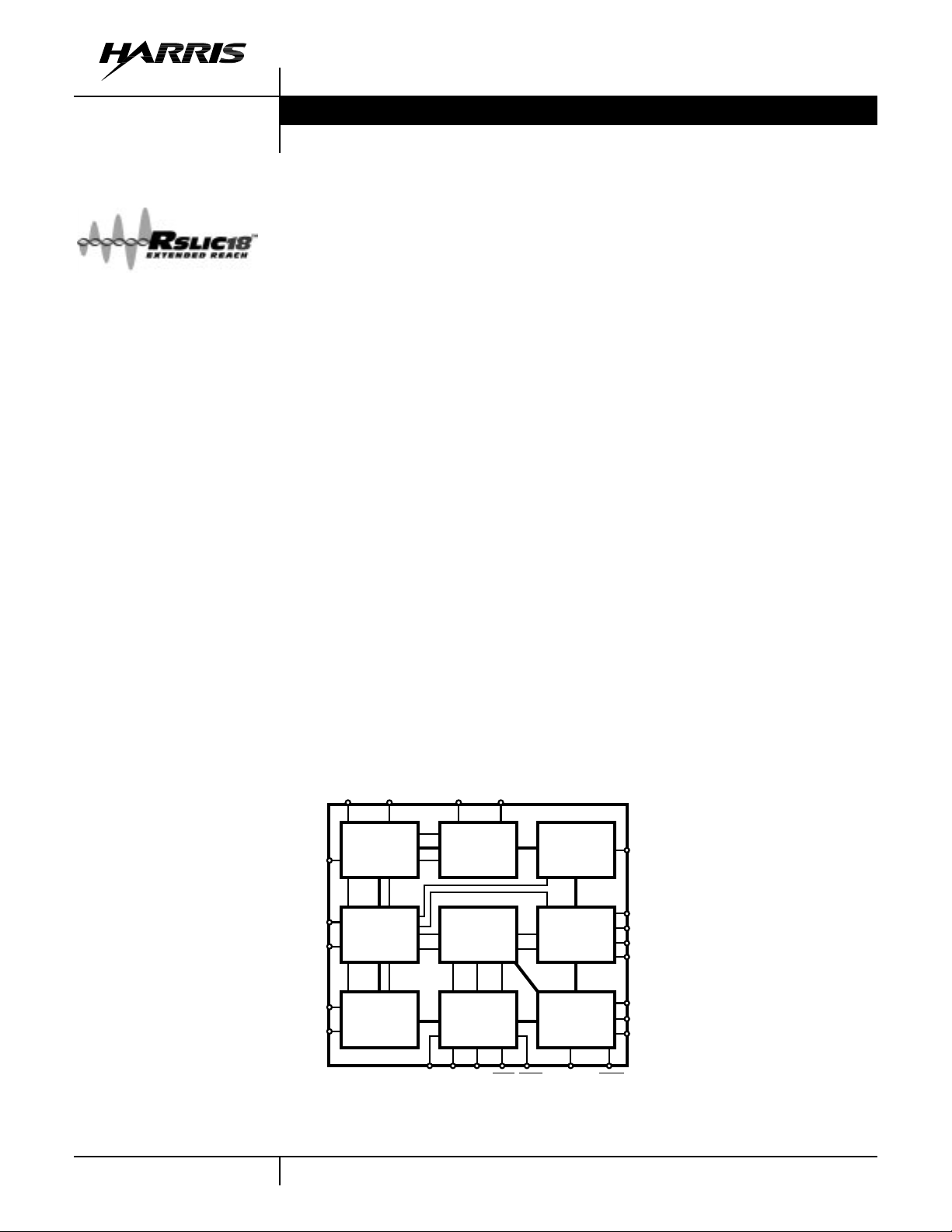
Block Diagram
4-80
POL CDC VBHVBL
DC
ILIM
TIP
RING
SW+
SW-
CONTROL
2-WIRE
PORT
TEST
ACCESS
BATTERY
SWITCH
TRANSMIT
SENSING
DETECTOR
LOGIC
RTD RD
CAUTION: These devices are sensitive to electrostatic discharge; follow proper IC Handling Procedures.
E0
DET ALM
RINGING
PORT
4-WIRE
PORT
CONTROL
LOGIC
BSEL
1-800-4-HARRIS or 407-727-9207
VRS
VRX
VTX
-IN
VFB
F2
F1
F0
SWC
RSLIC18™ is a trademark of Harris Corporation.
| Copyright © Harris Corporation 1999
Page 2
HC5549
Ordering Information (PLCC Package Only)
BATSWPOL
PART NUMBER 48V
HC5549CM ••
HC5549IM
•
•
REV
•
•
RING
DELAY
DRIVER
•
•
2W
LOOP
BACK LB = 53dB
••
••
TEMP.
RANGEoC PACKAGE
PACKAGE
NO.
0 to 70 28 Ld PLCC N28.45
-40 to 85 28 Ld PLCC N28.45
Device Operating Modes
OPERATING MODE F2 F1 F0 E0 = 1 E0 = 0 DESCRIPTION
Low Power Standby 0 0 0 SHD GKD MTU compliant standby mode with active loop
detector.
Forward Active 0 0 1 SHD GKD Forward battery loop feed.
Unused 0 1 0 n/a n/a Reserved internal test mode.
Reverse Active 0 1 1 SHD GKD Reverse battery loop feed.
Ringing 1 0 0 RTD RTD Enabler internal ring trip detector.
Unused 1 0 1 n/a n/a Reserved internal test mode.
Unused 1 1 0 n/a n/a Reserved internal test mode.
Power Denial 1 1 1 n/a n/a Device shutdown.
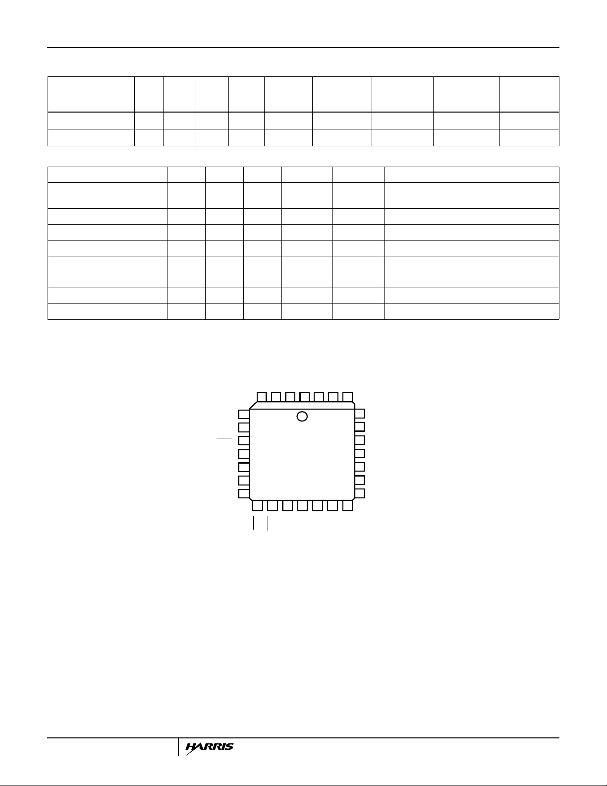
Pinouts
HC5549 (PLCC)
TOP VIEW
SW+
SW-
SWC
F2
F1
F0
E0
RD
RING
NC
ILIM
27
26
RTD
25
CDC
24
V
23
CC
22
-IN
VFB
21
VTX
20
VRX
19
17
18
VRB
POL
TIP
VBL
VBH
13
3
ALM
14
BGND
15
AGND
12
28
16
NC
4
5
6
7
8
9
10
11
12
DET
4-81
Page 3
HC5549
Absolute Maximum Ratings T
Maximum Supply Voltages
VCC . . . . . . . . . . . . . . . . . . . . . . . . . . . . . . . . . . . . . -0.5V to +7V
VCC - V
Uncommitted Switch Voltage. . . . . . . . . . . . . . . . . . . . . . . . . . -80V
ESD (Human Body Model). . . . . . . . . . . . . . . . . . . . . . . . . . . . 500V
. . . . . . . . . . . . . . . . . . . . . . . . . . . . . . . . . . . . . . . 80V
BAT
Operating Conditions
Temperature Range
Industrial (I suffix). . . . . . . . . . . . . . . . . . . . . . . . . . -40oC to 85oC
Commercial (C suffix). . . . . . . . . . . . . . . . . . . . . . . . 0oC to 75oC
Positive Power Supply (VCC). . . . . . . . . . . . . . . . . . . . . . . +5V ±5%
Negative Power Supply (VBH, VBL) (180, 181, 182) . . -16V to -80V
Uncommitted Switch (loop back or relay driver). . . . . . . +5V to -80V
CAUTION: Stresses above those listed in “Absolute Maximum Ratings” may cause permanent damage to the device. This is a stress only rating and operationofthe
device at these or any other conditions above those indicated in the operational sections of this specification is not implied.
NOTE:
1. θJA is measured with the component mounted on an evaluation PC board in free air.
Electrical Specifications Unless Otherwise Specified, T
PARAMETER TEST CONDITIONS MIN TYP MAX UNITS
RINGING PARAMETERS
VRB Input Impedance 480 - - kΩ
AC TRANSMISSION PARAMETERS (Forward Active and Reverse Active, BSEL = 0, unless otherwise specified.)
Receive Input Impedance 160 - - kΩ
Transmit Output Impedance --1Ω
4-Wire Port Overload Level THD = 1% 3.1 3.5 - V
2-Wire Port Overload Level THD = 1% 3.1 3.5 - V
2-Wire Return Loss 300Hz ≤ f < 1kHz 30 45 - dB
Longitudinal Current Capability (Per Wire) Test for False Detect - 20 - mA
2-Wire Longitudinal Balance Tested per IEEE455-1985, with 368Ω per wire. 53 - - dB
4-Wire Longitudinal Balance Tested per IEEE455-1985, with 368Ω per wire. 59 - - dB
4-Wire to 4-Wire Insertion Loss -6.22 -6.02 -5.82 dB
2-Wire to 4-Wire Level Linearity
4-Wire to 2-Wire Level Linearity
Referenced to -10dBm
Idle Channel Noise 2-Wire C-Message - 16 19 dBrnC
DC PARAMETERS
Loop Current Limit Programming Range Max Low Battery = -52V, BSEL = 0 15 - 45 mA
Loop Current Accuracy I
Loop Current During Low Power Standby Forward polarity only. 17 - 26 mA
Open Circuit Voltage
(|Tip - Ring|)
Low Power Standby Open Circuit Voltage (Tip - Ring) BSEL = 1 43 45 47 V
Ring Trip Programming Current Accuracy - - 10 %
=25oC Thermal Information
A
Thermal Resistance (Typical, Note 1) θJA(oC/W)
PLCC Package. . . . . . . . . . . . . . . . . . . . . . . . . . . . . 53
Maximum Junction Temperature Plastic . . . . . . . . . . . . . . . . 150oC
Maximum Storage Temperature Range. . . . . . . . . . -65oC to 150oC
Maximum Lead Temperature (Soldering 10s) . . . . . . . . . . . . 300oC
(PLCC - Lead Tips Only)
Die Characteristics
Substrate Potential. . . . . . . . . . . . . . . . . . . . . . . . . . . . . . . . . . V
Process . . . . . . . . . . . . . . . . . . . . . . . . . . . . . . . . . . . . . . Bipolar-DI
= -40oC to 85oC, VBL = -24V, VBH= -48V, VCC = +5V, AGND = BGND = 0V , loop
current limit = 25mA. All AC Parameters are specified at 600Ω 2-wire terminating impedance over the frequency
band of 300Hz to 3.4kHz. Protection resistors = 0Ω.
A
PK
PK
1kHz ≤ f ≤ 3.4kHz 35 45 - dB
RMS
Test forFalseDetect,Low PowerStandby, BSEL=0 - 10 - mA
+3 to -40dBm, 1kHz - 0.025 - dB
-40 to -50dBm, 1kHz - 0.050 - dB
-50 to -55dBm, 1kHz - 0.100 - dB
Psophometric - -74 -71 dBmp
= 25mA, BSEL = 0 - - 10 %
L
BSEL = 0 14 15.5 17 V
BSEL = 1 37.5 40 42.5 V
RMS
BAT
4-82
Page 4

HC5549
Electrical Specifications Unless Otherwise Specified, T
= -40oC to 85oC, VBL = -24V, VBH= -48V, VCC = +5V, AGND = BGND = 0V , loop
A
current limit = 25mA. All AC Parameters are specified at 600Ω 2-wire terminating impedance over the frequency
band of 300Hz to 3.4kHz. Protection resistors = 0Ω. (Continued)
PARAMETER TEST CONDITIONS MIN TYP MAX UNITS
Ground Key Threshold 10 12 13.5 mA
o
Thermal Alarm Output IC junction temperature - 175 -
C
RELAY DRIVER
On Voltage I
= 45 mA - - 0.60 V
L
LOGIC INPUTS (F0, F1, F2, E0, SWC)
Input Low Voltage - - 0.8 V
Input High Voltage 2.0 - - V
Input Low Current V
Input High Current V
LOGIC OUTPUTS (
DET, ALM)
Output Low Voltage I
Output High Voltage I
= 0.4V -20 - - µA
IL
= 2.4V - - 5 µA
IH
= 5mA - - 0.4 V
OL
= 100 µA 2.4 - - V
OH
SUPPLY CURRENTS (Supply currents not listed are considered negligible and do not contribute significantly to total power dissipation. All
measurements made under open circuit load conditions.)
Low Power Standby I
Forward or Reverse (Note 5) I
Forward I
Power Denial I
CC
, BSEL = 1 - 0.375 0.600 mA
I
BH
CC
I
, BSEL = 0 - 1.0 2.0 mA
BL
CC
, BSEL = 1 - 0.7 1.5 mA
I
BL
I
, BSEL = 1 - 1.0 2.0 mA
BH
CC
, BSEL = 1 or 0 - 0.2 0.5 mA
I
BL
2.0 3.7 5.0 mA
2.5 4.0 5.0 mA
3.5 4.5 6.5 mA
0.5 3.0 5.0 mA
ON HOOK POWER DISSIPATION
Forward or Reverse BSEL = 0 - 44 60 mW
Forward or Reverse BSEL = 1 - 90 150 mW
Low Power Standby BSEL = 1 - 37 60 mW
OFF HOOK POWER DISSIPATION
Forward or Reverse BSEL = 0 - 290 310 mW
POWER SUPPLY REJECTION RATIO
V
to 2-Wire f = 300Hz - 40 - dB
CC
f = 1kHz - 35 - dB
f = 3.4kHz - 28 - dB
to 4-Wire f = 300Hz - 45 - dB
V
CC
f = 1kHz - 43 - dB
f = 3.4kHz - 33 - dB
to 2-Wire 300Hz ≤ f ≤ 3.4kHz - 30 - dB
V
BL
V
to 4-Wire 300Hz ≤ f ≤ 3.4kHz - 35 - dB
BL
to 2-Wire 300Hz ≤ f ≤ 3.4kHz - 33 - dB
V
BH
to 4-Wire 300Hz ≤ f ≤ 1kHz - 40 - dB
V
BH
1kHz < f ≤ 3.4kHz - 45 - dB
4-83
Page 5

HC5549
Design Equations
Loop Supervision Thresholds
SWITCH HOOK DETECT
The switch hook detect threshold is set by a single e xternal
resistor, RSH. Equation 1 is used to calculate the value of RSH.
R
600 ISH⁄=
SH
The term I
is the desired DC loop current threshold. The
SH
loop current threshold programming range is from 5mA to
15mA.
GROUND KEY DETECT
The ground key detector senses a DC current imbalance
between the Tip and Ring terminals when the ring terminal is
connected to ground. The ground key detect threshold is not
externally programmable and is internally fixed to 12mA
regardless of the switch hook threshold.
RING TRIP DETECT
The ring trip detect threshold is set by a single external
resistor, R
. IRT should be set between the peak ringing
RT
current and the peak off hook current while still ringing.
R
1800 IRT⁄=
RT
The capacitor C
, in parallel with RRT, will set the ring trip
RT
response time.
Loop Current Limit
The loop current limit of the device is programmed by the
external resistor R
using Equation 3.
1760
R
------------ -=
IL
I
LIM
. The value of RIL can be calculated
IL
(EQ. 1)
(EQ. 2)
(EQ. 3)
4-WIRE TO 2-WIRE GAIN
The 4-wire to 2-wire gain is defined as the receive gain. It is
a function of the terminating impedance, synthesized
impedance and protection resistors. Equation 6 calculates
the receive gain, G
G
42
----------------------------------------- -
2
–=
ZO+2RP+Z
.
42
Z
L
L
(EQ. 6)
When the device source impedance and protection resistors
equals the terminating impedance, the receive gain equals
unity.
2-WIRE TO 4-WIRE GAIN
The 2-wire to 4-wire gain (G
) is the gain from tip and ring to
24
the VTX output. The transmit gain is calculated in Equation 7.
Z
G
–=
24
O
----------------------------------------- -
ZO+2RP+Z
(EQ. 7)
L
When the protection resistors are set to zero, the transmit
gain is -6dB.
TRANSHYBRID GAIN
The transhybrid gain is defined as the 4-wire to 4-wire gain
(G
).
44
Z
G
44
ZO2RPZ
++
L
O
---------------------------------------
–=
(EQ. 8)
When the protection resistors are set to zero, the transhybrid
gain is -6dB.
COMPLEX IMPEDANCE SYNTHESIS
Substituting the impedance programmingresistor,R
, with a
S
complex programming network provides complex
impedance synthesis.
The term I
is the desired loop current limit. The loop
LIM
current limit programming range is from 15mA to 45mA.
Impedance Matching
The impedance of the device is programmed with the
external component R
the feedback amplifier that provides impedance matching. If
complex impedance matching is required, then a complex
network can be substituted for R
RESISTIVE IMPEDANCE SYNTHESIS
The source impedance of the device, Z
in Equation 4.
RS400 ZO()=
The required impedance is defined by the terminating
impedance and protection resistors as shown in Equation 5.
Z
–=
OZL2RP
. RS is the gain setting resistor for
S
.
S
, can be calculated
O
4-84
(EQ. 4)
(EQ. 5)
2-WIRE
NETWORK
C
2
R
1
R
2
FIGURE 1. COMPLEX PROGRAMMING NETWORK
PROGRAMMING
NETWORK
C
P
R
S
R
P
The reference designators in the programming network
match the evaluation board. The component R
different design equation than the R
used for resistive
S
has a
S
impedance synthesis. The design equations for each
component are provided below.
RS400 R12RP()–()×=
RP400 R2×=
C
PC2
400⁄=
(EQ. 10)
(EQ. 11)
(EQ. 9)
Page 6

HC5549
Low Power Standby
Overview
The low power standby mode (LPS, 000) should be used
during idle line conditions. The device is designed to operate
from the high battery during this mode. Most of the internal
circuitry is powered down, resulting in low power dissipation.
If the 2-wire (tip/ring) DC voltage requirements are not
critical during idle line conditions, the device may be
operated from the low battery. Operation from the low
battery will decrease the standby power dissipation.
TABLE 1. DEVICE INTERFACES DURING LPS
INTERFACE
Receive x AC transmission, impedance
Ringing x
Transmit x
2-Wire x Amplifiers disabled.
Loop Detect x Switch hook or ground key.
2-WIRE INTERFACE
During LPS, the 2-wire interface is maintained with internal
switches and voltage references. The Tip and Ring
amplifiers are turned off to conserve power. The device will
provide MTU compliance, loop current and loop supervision.
Figure 2 represents the internal circuitry providing the 2-wire
interface during low power standby.
FIGURE 2. LPS 2-WIRE INTERFACE CIRCUIT DIAGRAM
MTU Compliance
Maintenance Termination Unit or MTU compliance places
DC voltage requirements on the 2-wire terminals during idle
line conditions. The minimum idle voltage is 42.75V. The
high side of the MTU range is 56V. The voltage is expressed
as the difference between Tip and Ring.
The Tip voltage is held near ground through a 600Ω resistor
and switch. The Ring voltage is limited to a maximum of
-49V (by MTU REF) when operating from either the high or
low battery. A switch and 600Ω resistor connect the MTU
reference to the Ring terminal. When the high battery
voltage exceeds the MTU reference of -49V (typically), the
ON OFF NOTES
matching and ringing are disabled during this mode.
GND
600Ω
TIP AMP
TIP
RING
RING AMP
600Ω
MTU REF
Ring terminal will be clamped by the internal reference. The
same Ring relationships apply when operating from the low
battery voltage. For high battery voltages (VBH) less than or
equal to the internal MTU reference threshold:
V
RINGVBH
4+=
(EQ. 12)
Loop Current
During LPS, the device will provide current to a load. The
current path is through resistors and switches, and will be
function of the off hook loop resistance (R
LOOP
). This
includes the off hook phone resistance and copper loop
resistance. The current available during LPS is determined
by Equation 13.
I
LOOP
1– 49–()–()600 600 R
++()⁄=
LOOP
(EQ. 13)
Internal current limiting of the standby switches will limit the
maximum current to 20mA.
Another loop current related parameter is longitudinal
current capability. The longitudinal current capability is
reduced to 10mA
per pin. The reduction in longitudinal
RMS
current capability is a result of turning off the Tip and Ring
amplifiers.
On Hook Power Dissipation
The on hook power dissipation of the device during LPS is
determined by the operating voltages and quiescent currents
and is calculated using Equation 14.
P
LPSVBHIBHQ
× VBLI
× VCCI
BLQ
×++=
CCQ
(EQ. 14)
The quiescent current terms are specified in the electrical
tables for each operating mode. Load power dissipation is
not a factor since this is an on hook mode. Some
applications may specify a standby current. The standby
current may be a charging current required for modern
telephone electronics.
Standby Current Power dissipation
Any standby line current, I
power dissipation term P
power contribution is zero when the standby line current is
zero.
P
SLCISLCVBH
49– 1I
If the battery voltage is less than -49V (the MTU clamp is
off), the standby line current power contribution reduces to
Equation 16.
P
SLCISLCVBH
1I
Most applications do not specify charging current
requirements during standby. When specified, the typical
charging current may be as high as 5mA.
, introduces an additional
SLC
. Equation 15 illustrates the
SLC
x1200++()×=
SLC
x1200++()×=
SLC
(EQ. 15)
(EQ. 16)
4-85
Page 7

HC5549
Forward Active
Overview
The forward active mode (FA, 001) is the primary AC
transmission mode of the device. On hook transmission, DC
loop feed and voice transmission are supported during forward
active. Loop supervision is provided by either the switch hook
detector (E0 = 1) or the ground key detector (E0= 0). The
device may be operated from either high or lo w battery for onhook transmission and low battery for loop feed.
On-Hook Transmission
The primary purpose of on hook transmission will be to
support caller ID and other advanced signalling features.
The transmission over load levelwhile on hook is 3.5V
When operating from the high battery, the DC voltages at Tip
and Ring are MTU compliant. The typical Tip voltage is -4V
and the Ring voltage is a function of the battery voltage for
battery voltages less than -60V as shown in Equation 17.
V
RINGVBH
4+=
Loop supervision is provided by the switch hook detector at
the
DET output. When DET goes low, the low battery should
be selected for DC loop feed and voice transmission.
Feed Architecture
The design implements a voltage feed current sense
architecture. The device controls the voltage across Tip and
Ring based on the sensing of load current. Resistors are
placed in series with Tip and Ring outputs to provide the
current sensing. The diagram below illustrates the concept.
R
B
R
V
OUT
R
L
FIGURE 3. VOLTAGE FEED CURRENT SENSE DIAGRAM
CS
-
+
-
+
K
S
R
A
By monitoring the current at the amplifier output, a negative
feedback mechanism sets the output voltage for a defined
load. The amplifier gains are set by resistor ratios (R
R
) providing all the performance benefits of matched
C
resistors. The internal sense resistor, R
, is much smaller
CS
than the gain resistors and is typically 20Ω for this device.
The feedback mechanism, K
, represents the amplifier
S
configuration providing the negative feedback.
DC Loop Feed
The feedback mechanism for monitoring the DC portion of
the loop current is the loop detector. A low pass filter is used
in the feedback to block voice band signals from interfering
with the loop current limit function. The pole of the low pass
PEAK
(EQ. 17)
V
IN
R
C
, RB,
A
filter is set by the external capacitor C
. The value of the
DC
external capacitor should be 4.7µF.
Most applications will operate the device from low battery
while off hook. The DC feed characteristic of the device will
drive Tip and Ring towards half battery to regulate the DC
loop current. For light loads, Tip will be near -4V and Ring
will be near V
+ 4V. The following diagram shows the DC
VBL
feed characteristic.
V
TR(OC)
, DC (V)
TR
.
V
(mA)
I
FIGURE 4. DC FEED CHARACTERISTIC
LOOP
The point on the y-axis labeled V
m = (∆VTR/∆IL) = 10kΩ
I
LIM
is the open circuit
TR(OC)
Tip to Ring voltage and is defined by the feed battery
voltage.
V
TR OC()VBL
8–=
(EQ. 18)
The curve of Figure 5 determines the actual loop current for
a given set of loop conditions. The loop conditions are
determined by the low battery voltage and the DC loop
impedance. The DC loop impedance is the sum of the
protection resistance, copper resistance (ohms/foot)and the
telephone off hook DC resistance.
I
A
I
B
R
(Ω)
KNEE
LOAD CHARACTERISTIC
FIGURE 5. I
I
(mA)
LOOP
I
LOOP
SC
I
LIM
2R
P
VERSUS R
R
LOOP
LOOP
The slope of the feed characteristic and the battery voltage
define the maximum loop current on the shortest possible
loop as the short circuit current I
I
SCILIM
The term I
V
------------------------------------------------------+=
is the programmed current limit, 1760/RIL.
LIM
The line segment I
–
TR OC()2RPILIM
10e3
represents the constant current region
A
SC
.
(EQ. 19)
of the loop current limit function.
IAI
LIM
V
--------------------------------------------------------------+=
–
TR OC()RLOOPILIM
10e3
(EQ. 20)
The maximum loop impedance for a programmed loop
current is defined as R
V
TR OC()
R
KNEE
------------------------=
I
LIM
KNEE
.
(EQ. 21)
4-86
Page 8

HC5549
When R
is exceeded, the device will transition from
KNEE
constant current feedto constant voltage,resistive feed. The
line segment I
represents the resistive feed portion of the
B
load characteristic.
V
I
B
TR OC()
------------------------=
R
LOOP
(EQ. 22)
Voice Transmission
The feedback mechanism for monitoring the AC portion of
the loop current consists of two amplifiers, the sense
amplifier (SA) and the transmit amplifier (TA). The AC
feedback signal is used for impedance synthesis. A detailed
model of the AC feed back loop is provided below.
T
SA
R
VRX
R
VTX
A
+
-
8K
R
S
-IN
C
FB
VFB
TIP
RING
R
20
20
-
+
+
-
R
3R
3R
3R
3R
1:1
0.75R
-
+
R/2
V
The AC feed back loop produces an echo at the V
of the signal injected at V
. The echo must be cancelled to
RX
TX
output
maintain voice quality. Most applications will use a summing
amplifier in the CODEC front end as shown below to cancel
the echo signal.
R
VRX
R
1:1
VTX
T
A
+
-
HC5518x
FIGURE 7. TRANSHYBRID BALANCE INTERFACE
The resistor ratio, R
the transmit gain, G
R
S
-IN
, provides the final adjustment for
F/RB
. The transmit gain is calculated using
TX
R
A
R
F
R
B
-
+
+2.4V
RX OUT
TX IN
CODEC
Equation 25.
R
F
G
=
TX
Most applications set R
G–
------- -
24
R
B
= RB, hence the device 2-wire to
F
4-wire equals the transmit gain. Typically R
is greater than
B
(EQ. 25)
20kΩ to prevent loading of the device transmit output.
FIGURE 6. AC SIGNAL TRANSMISSION MODEL
The gain of the transmit amplifier, set by R
programmed impedance of the device. The capacitor C
, determines the
S
FB
blocks the DC component of the loop current. The ground
symbols in the model represent AC grounds, not actual DC
potentials.
The sense amp output voltage, V
, as a function of Tip and
SA
Ring voltage and load is calculated using Equation 23.
10
=
V
SA
VTVR–()–
------
Z
L
(EQ. 23)
The transmit amplifier provides the programmable gain
required for impedance synthesis. In addition, the output of
this amplifier interfaces to the CODEC transmit input. The
output voltage is calculated using Equation 24.
V
VTX
–=
V
----------
SA
8e3
(EQ. 24)
R
S
Once the impedance matching components have been
selected using the design equations, the above equations
provide additional insight as to the expected AC node
voltages for a specific Tip and Ring load.
Transhybrid Balance
The final step in completing the impedance synthesis design
is calculating the necessary gains for transhybrid balance.
The resistor ratio, R
gain of the device, G
transmit gain requirement and R
, is determined by the transhybrid
F/RA
. RF is previously defined by the
44
is calculated using
A
Equation 26.
R
B
----------=
R
A
G
44
(EQ. 26)
Power Dissipation
The power dissipated by the device during on hook
transmission is strictly a function of the quiescent currents
for each supply voltage during Forward Active operation.
P
FAQVBH
BHQ
× VCCI
BLQ
×++=
CCQ
I×
VBLI
Off hook power dissipation is increased above the quiescent
power dissipation by the DC load. If the loop length is less
than or equal to R
current, I
, and the power dissipation is calculated using
A
, the device is providing constant
KNEE
Equation 28.
P
FA IA()PFA Q()VBLxIA
()R
If the loop length is greaterthan R
()–+=
KNEE
2
xI
LOOP
A
, the device is operating
in the constant voltage, resistive feed region. The power
dissipated in this region is calculated using Equation 29.
P
FA IB()PFA Q()VBLxIB
()R
()–+=
LOOP
2
xI
B
(EQ. 27)
(EQ. 28)
(EQ. 29)
4-87
Page 9

HC5549
Since the current relationships are different for constant
current versus constant voltage, the region of device
operation is critical to valid power dissipation calculations.
Reverse Active
Overview
The reverse active mode (RA, 011) provides the same
functionality as the forward active mode. On hook
transmission, DC loop feed and voice transmission are
supported. Loop supervision is provided by either the switch
hook detector (E0 = 1) or the ground key detector (E0 = 0).
The device may be operated from either high or low battery.
During reverse active the Tip and Ring DC voltage
characteristics exchange roles. That is, Ring is typically 4V
below ground and Tip is typically 4V more positive than
battery. Otherwise, all feed and voice transmission
characteristics are identical to forward active.
Silent Polarity Reversal
Changing from forward active to reverse active or vice versa
is referred to as polarity reversal. Many applications require
slew rate control of the polarity reversalevent. Requirements
range from minimizing cross talk to protocol signalling.
The device uses an external low voltage capacitor, C
set the reversal time. Once programmed, the reversal time
will remain nearly constant over various load conditions. In
addition, the reversal timing capacitor is isolated from the AC
loop, therefore loop stability is not impacted.
The internal circuitry used to set the polarity reversal time is
shown below.
I
1
POL
75kΩ
I
2
C
POL
POL
,to
POL pin and minimal voltage excursion ±0.75V, are well
suited to polarized capacitors.
Power Dissipation
The power dissipation equations for forwardactive operation
also apply to the reverse active mode.
Ringing
Overview
The ringing mode (RNG, 100) provides the low side return
path for externally supplied battery backed ringing. The
ringing signal must be injected through a relay at the ring
terminal. The device should be operated from the low battery
voltage during this mode to minimize the overall power
dissipation during ringing. Current flowing through the Tip
terminal will provide the necessary ring trip information.
Ringing Bias Input
The ringing bias input, VRB, is a high impedance input. The
VRB input is only selected during the ringing mode. The gain
from the VRB input to the Tip output is typically 40V/V. The
following equation shows the relationship of the Tip output
voltage to the VRB input voltage.
VBL
----------- - 40 VRB×+=
V
TIP
2
A positive DC voltage at VRB is required to shift the Tip
output voltage towards ground to provide the low side ringing
return path. Tying the logic input F2 to VRB provides the
positive voltage to offset Tip during ringing. A voltage divider
is suggested to provide control the actual voltage applied to VRB.
Logic Control
Ringing patterns consist of silent intervals. The ringing to
silent pattern is called the ringing cadence. During the silent
portion of ringing, the device can be programmed to any
other operating mode. The most likely candidates are low
power standby or forward active. Depending on system
requirements, the low or high battery may be selected.
(EQ. 31)
FIGURE 8. REVERSAL TIMING CONTROL
During forward active,the current from source I1 charges the
external timing capacitor C
and the switch is open. The
POL
internal resistor provides a clamping function for voltages on
the POL node. During reverse active, the switch closes and
I2 (roughly twice I1) pulls current from I1 and the timing
capacitor. The current at the POL node provides the drive to
a differential pair which controls the reversal time of the Tip
and Ring DC voltages.
C
POL
∆time
----------------=
75000
(EQ. 30)
Where ∆time is the required reversal time. Polarized
capacitors may be used for C
. The low voltage at the
POL
4-88
Loop supervision is provided with the ring trip detector. The
ring trip detector senses the change in loop current when the
phone is taken off hook. The loop detector full wave rectifies
the ringing current, which is then filtered with external
components RRT and CRT. The resistor RRT sets the trip
threshold and the capacitor CRT sets the trip response time.
Most applications will require a trip response time less than
150 milliseconds.
Three very distinct actions occur when the devices detects a
ring trip. First, the
DET output is latched low. The latching
mechanism eliminates the need for software filtering of the
detector output. The latch is cleared when the operating
mode is changed externally. Second, the VRS input is
disabled,removing the Tip biasing signal from the line. Third,
the device is internally forced to the forward active mode.
Page 10

HC5549
Power Dissipation
The power dissipation during ringing is dictated by the load
driving requirements and the ringing waveform. The key to
valid power calculations is the correct definition of average
and rms currents. The average current defines the high
battery supply current. The rms current defines the load
current.
The cadence provides a time averaging reduction in the
peak power. The total power dissipation consists of ringing
power, P
P
RNGPr
, and the silent interval power, Ps.
r
t
r
--------------
⋅ P
trts+
t
s
--------------
⋅+=
s
trts+
(EQ. 32)
The terms, tr and ts, represent the cadence. The ringing
interval is tr and the silent interval is ts. The typical cadence
ratio tr:ts is 1:2.
The quiescent power of the device in the ringing mode is
defined in Equation 34.
P
rQ()
VBH IBH
⋅ VBL IBLQ⋅ VCC ICC
Q
⋅++=
Q
(EQ. 33)
During ringing, the device is operated from the low battery,
therefore the VBH power contribution is negligible. The total
power during the ringing interval is the sum of the quiescent
power and loading power:
2
V
P
rPrQ()
VBL I
⋅
AVG
rms
------------------------------------------–+=
Z
+
RENRLOOP
For sinusoidal waveforms, the average current, I
AVG
(EQ. 34)
, is
defined in equation 36.
I
AVG
2
-- -
------------------------------------------
=
π
Z
V
RENRLOOP
rms
2⋅
+
(EQ. 35)
The only amplifier providing load current during ringing is the
Tip amplifier. Therefore the total power contribution from the
device is half the average power required by the load.
I
AVG
1
-- -
------------------------------------------
=
π
Z
V
RENRLOOP
rms
2⋅
+
(EQ. 36)
The silent interval power dissipation will be determined by
the quiescent power of the selected operating mode.
Power Denial
Overview
The power denial mode (111) will shutdown the entire device
except for the logic interface. Loop supervision is not
provided. This mode may be used as a sleep mode or to
shutdown in the presence of a persistent thermal alarm.
Switching between high and low battery will have no effect
during power denial.
Functionality
During power denial, both the Tip and Ring amplifiers are
disabled, representing high impedances. The voltages at
both outputs are near ground.
Thermal Shutdown
In the event the safe die temperature is exceeded, the ALM
output will go low and
automatically shut down. When thedevicecools,
high and
persists,
DET will reflect the loop status. If the thermal fault
ALM will go low again and the part will shutdown.
DET will go high and the part will
ALM will go
Programming power denial will permanently shutdown the
device and stop the self cooling cycling.
Battery Switching
Overview
The integrated battery switch selects between the high
battery (VBH) and low battery (VBL). The battery switch is
controlled with the logic input BSEL. When BSEL is a logic
high, the high battery is selected and when a logic low, the
low battery is selected. All operating modes of the device will
operate from high or low battery except forward loop back.
Functionality
The logic control is independent of the operating mode
decode. Independent logic control provides the most
flexibility and will support all application configurations.
When changing device operating states, battery switching
should occur simultaneously with or prior to changing the
operating mode. In most cases, this will minimize overall
power dissipation and prevent glitches on the
The only external component required to support the battery
switch is a diode in series with the VBH supply lead. In the
event that high battery is removed, the diode allows the
device to transition to low battery operation.
Low Battery Operation
All off hook operating conditions and ringing should use the
low battery. The prime benefit will be reduced power
dissipation. The typical low battery for the device is -24V.
However this may be increased to support longer loop
lengths or high loop current requirements. Standby
conditions may also operate from the low battery if MTU
compliance is not required, further reducing standby power
dissipation.
High Battery Operation
The high battery should be used for standby conditions
which must provide MTU compliance. During standby
operation the power consumption is typically 40 mW with 48V battery. If standby requirements do not require high
battery operation, then a lower battery will result in lower
standby power.
DET output.
4-89
Page 11

HC5549
Uncommitted Switch
Overview
The uncommitted switch is a three terminal device designed
for flexibility. The independent logic control input,
allows switch operation regardless of device operating
mode. The switch is activated by a logic low. The positive
and negative terminals of the device are labeled SW+ and
SW- respectively.
Relay Driver
The uncommitted switch may be used as a relay driver by
connecting SW+ to the relay coil and SW- to ground. The
switch is designed to have a maximum on voltage of 0.6V
with a load current of 45mA.
+5V
RELAY
SW+
SW-
FIGURE 9. EXTERNAL RELAY SWITCHING
Since the device provides the ringing waveform, the relay
functions which may be supported include subscriber
disconnect, test access or line interface bypass. An external
SWC,
SWC
snubber diode is not required when using the uncommitted
switch as a relay driver.
Test Load
The switch may be used to connect test loads across Tip
and Ring. The test loads can provide external test
termination for the device. Proper connection of the
uncommitted switch to Tip and Ring is shown below.
TIP
RING
TEST
LOAD
SW+
SW-
FIGURE 10. TEST LOAD SWITCHING
The diode in series with the test load blocks current from
flowing through the uncommitted switch when the polarity of
the Tip and Ring terminals are reversed. In addition to the
reverseactive state, the polarity of Tip and Ring are reversed
for half of the ringing cycle. With independent logic control
and the blocking diode, the uncommitted switch may be
continuously connected to the Tip and Ring terminals.
SWC
4-90
Page 12

Basic Application Circuit
HC5549
CPS1
CPS2
RP1
RP2
PROTECTION
NETWORK
-48V
VCC
CPS3
CRT
RRT
RSH
RIL
CDC
CPOL
CIL
VCC
TIP
HC5549
RING
SW+
SW-
RTD
RD
ILIM
CDC
POL
VBL
U1
VBH
SWC
BSEL
BGNDAGND
VRX
VRB
VTX
-IN
VFB
E0
F0
F1
F2
DET
ALM
D1
RS
CRX
CTX
CFB
RB1
RB2
FIGURE 11. HC5549 BASIC APPLICATION CIRCUIT
Basic Application Circuit Component List
COMPONENT VALUE TOLERANCE RATING COMPONENT VALUE TOLERANCE RATING
U1 HC5549 N/A N/A n/a n/a n/a n/a
RRT 20kΩ 1% 0.1W CDC 4.7µF 20% 10V
RSH 49.9kΩ 1% 0.1W CPS1 0.1µF 20% >100V
RIL 71.5kΩ 1% 0.1W CPS2, CPS3 0.1µF 20% 100V
RS 210kΩ 1% 0.1W D1 1N400X type with breakdown > 100V.
CRX, CRS, CTX, CRT,
CPOL, CFB
Design Parameters: Ring Trip Threshold = 90 mA peak., Switch Hook Threshold = 12 mA, Loop Current Limit = 24.6 mA, Synthesize Device
Impedance = 210kΩ/400= 525Ω, with 39Ω protection resistors, impedance across Tip and Ring terminals = 603Ω.
0.47µF 20% 10V RP1, RP2 Protection resistor values are application
dependent and will be determined byprotection
requirements. Standard applications will use ≥
35Ω per side.
4-91
Page 13

HC5549
Pin Description
PLCC SYMBOL DESCRIPTION
1 TIP TIP power amplifier output.
2 BGND Battery Ground - To be connected to zero potential. All loop current and longitudinal current flow from this ground.
Internally separate from AGND but it is recommended that it is connected to the same potential as AGND.
3 VBL Low battery supply connection.
4 VBH High battery supply connection.
5 SW+ Uncommitted switch positive terminal.
6 SW- Uncommitted switch negative terminal.
7 SWC Switch control input. This TTL compatible input controls the uncommitted switch, with a logic “0” enabling the switch and
logic “1” disabling the switch.
8 F2 Mode control input - MSB. F2-F0 for the TTL compatible parallel control interface for controlling the various modes of
operation of the device.
9 F1 Mode control input.
10 F0 Mode control input.
11 E0 DetectorOutput Selection Input. This TTL inputcontrolsthe multiplexing of the SHD (E0=1) andGKD (E0 =0) comparator
outputs to the DET output based upon the state at the F2-F0 pins.
12 DET Detector Output - This TTL output provides hook status of the loop based upon the selected operating mode. The
detected output will either be switch hook, ground key or ring trip.
13 ALM Thermal Shutdown Alarm. This pin signals the internal die temperature has exceeded safe operating temperature and
the device has been powered down automatically.
14 AGND Analog ground reference. This pin should be externally connected to BGND.
15 BSEL Selects between high and low battery, with a logic “1” selecting the high battery and logic “0” the low battery.
16 NC This pin is a “no connect” and should remain floating proper device operation.
17 POL Capacitor connected to this pin sets the polarity reversal slew rate.
18 VRB Ringing Bias Input - Analog input to offset Tip output towards ground while in Ringing Mode.
19 VRX Analog Receive Voltage - 4-wire analog audio input voltage. AC couples to codec.
20 VTX Transmit output voltage - Output of impedance matching amplifier, AC couples to codec.
21 VFB Feedback voltage for impedance matching. This voltage is scaled to accomplish impedance matching.
22 -IN Impedance matching amplifier summing node.
23 VCC Positive voltage power supply.
24 CDC DC Biasing Filter Capacitor - Connects between this pin and VCC.
25 RTD Ring trip filter network.
26 ILIM Loop Current Limit programming resistor.
27 RD Switch hook detection threshold programming resistor.
28 RING RING power amplifier output.
4-92
 Loading...