

Page 1
T
www.BDTIC.com/Intersil
C
®
B
O
M
Data Sheet August 2003
O
EC
R
S
M
T
E
L
O
E
D
N
E
H
E
C
D
O
PR
R
D
5
5
C
A
PL
E
5
1
U
T
EN
M
E
HC5526
FN4151.8
ITU CO/PABX SLIC with Low Power
Standby
The HC5526 is a subscriber line interface circuit that is
compliant with CCITT standards. Enhancements include
immunity to circuit latch-up during hot plug and absence of
false signaling in the presence of longitudinal currents.
The HC5526 is fabricated in a High Voltage Dielectrically
Isolated (DI) Bipolar Process that eliminates leakage
currents and device latch-up problems normally associated
with Junction Isolated (JI) ICs. The elimination of the leakage
currents results in improved circuit performance for wide
temperature extremes. The latch free benefit of the DI
process guarantees operation under adverse transient
conditions. This process feature makes the HC5526 ideally
suited for use in harsh outdoor environments.
Part Number Information
PART NUMBER
HC5526CM 0 to 70 28 Ld PLCC N28.45
TEMP.
RANGE (oC) PACKAGE
PKG.
DWG. #
Features
• DI Monolithic High Voltage Process
• Programmable Current Feed . . . . . . . . . . . 20mA to 60mA
• Programmable Loop Current Detector Threshold and
Battery Feed Characteristics
• Ground Key and Ring Trip Detection
• Compatible with Ericsson’s PBL3764
• Thermal Shutdown
• On-Hook Transmission
• Wide Battery Voltage Range . . . . . . . . . . . . .-24V to -58V
• Low Standby Power
• Meets CCITT Transmission Requirements
o
• Ambient Temperature Range . . . . . . . . . . . -40
C to 85oC
Applications
• On-Premises (ONS)
•Key Systems
• PBX
• Related Literature
- AN9537, Operation of the HC5513/26 Evaluation Board
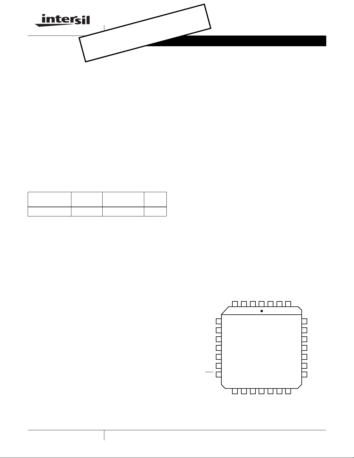
Pinout
HC5526 (PLCC)
TOP VIEW
RINGRLY
V
BAT
R
SG
E1
E0
N/C
DET
VCCN/C
5
6
7
8
9
10
11
12 13 14 15 16 17 18
C2
C1
BGND
1234
DC
R
SENSE
RING
AGND
RINGX
RSN
TIPX
N/C
SENSE
TIP
262728
25
DR
24
N/C
23
DT
22
RD
21
HPT
20
HPR
19
V
EE
V
TX
1
CAUTION: These devices are sensitive to electrostatic discharge; follow proper IC Handling Procedures.
1-888-INTERSIL or 321-724-7143
| Intersil (and design) is a registered trademark of Intersil Americas Inc.
All other trademarks mentioned are the property of their respective owners.
Copyright © Intersil Americas Inc. 2003. All Rights Reserved.
Page 2
HC5526
www.BDTIC.com/Intersil
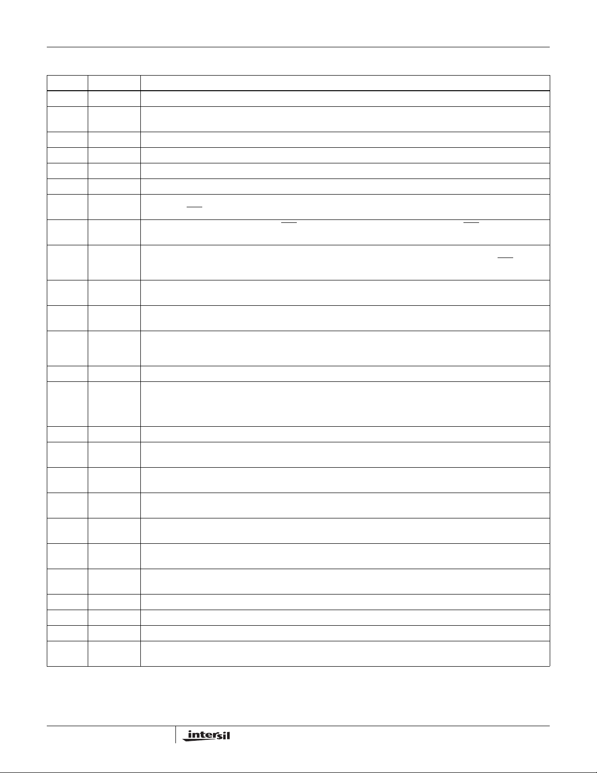
Pin Descriptions
PLCC SYMBOL DESCRIPTION
1RING
2 BGND Battery Ground - To be connected to zero potential. All loop current and longitudinal current flow from this ground.
4V
5 RINGRLY Ring relay driver output.
6V
7R
8 E1 TTL compatible logic input. The logic state of E1 in conjunction with the logic state of C1 determines which detector is
9 E0 TTL compatible logic input. Enables the DET
11 DET Detector output. TTL compatible logic output. A zero logic level indicates that the selected detector was triggered (see
12 C2 TTL compatible logic input. The logic states of C1 and C2 determine the operating states (Open Circuit, Active, Ringing
13 C1 TTL compatible logic input. The logic states of C1 and C2 determine the operating states (Open Circuit, Active, Ringing
14 R
15 AGND Analog ground.
16 RSN Receive Summing Node. The AC and DC current flowing into this pin establishes the metallic loop current that flows
18 V
19 V
20 HPR RING side of AC/DC separation capacitor C
21 HPT TIP side of AC/DC separation capacitor C
22 RD Loop current programming resistor. Resistor RD sets the trigger level for the loop current detect circuit. A filter capacitor
23 DT Input to ring trip comparator. Ring trip detection is accomplished by connecting an external network to a comparator in
25 DR Input to ring trip comparator. Ring trip detection is accomplished by connecting an external network to a comparator in
26 TIP
27 TIPX Output of tip power amplifier.
28 RINGX Output of ring power amplifier.
3, 10, 17,
24
SENSE
CC
BAT
SG
DC
EE
TX
SENSE
N/C No internal connection.
Internally connected to output of RING power amplifier.
Internally separate from AGND but it is recommended that it is connected to the same potential as AGND.
5V power supply.
Battery supply voltage, -24V to -56V.
Saturation guard programming resistor pin.
gated to the DET
a logic level one.
Truth Table for selection of Ground Key detector, Loop Current detector or the Ring Trip detector). The DET
an open collector with an internal pull-up of approximately 15kΩ to V
or Standby) of the SLIC.
or Standby) of the SLIC.
DC feed current programming resistor pin. Constant current feed is programmed by resistors R
connected in series from this pin to the receive summing node (RSN). The resistor junction point is decoupled to AGND
to isolate the AC signal components.
between tip and ring. The magnitude of the metallic loop current is 1000 times greater than the current into the RSN
pin. The constant current programming resistors and the networks for program receive gain and 2-wire impedance all
connect to this pin.
-5V power supply.
Transmit audio output. This output is equivalent to the TIP to RING metallic voltage. The network for programming the
2-wire input impedance connects between this pin and RSN.
loop current. The other end of C
current. The other end of C
is also connected between this pin and VEE.
C
D
the SLIC with inputs DT and DR.
the SLIC with inputs DT and DR.
Internally connected to output of tip power amplifier.
output.
is connected to HPT.
HP
is connected to HPR.
HP
HP
output when set to logic level zero and disables DET output when set to
CC.
and R
DC1
. C
HP
. C
is required to properly separate the ring AC current from the DC
HP
is required to properly separate the tip AC current from the DC loop
HP
DC2
output is
2
Page 3
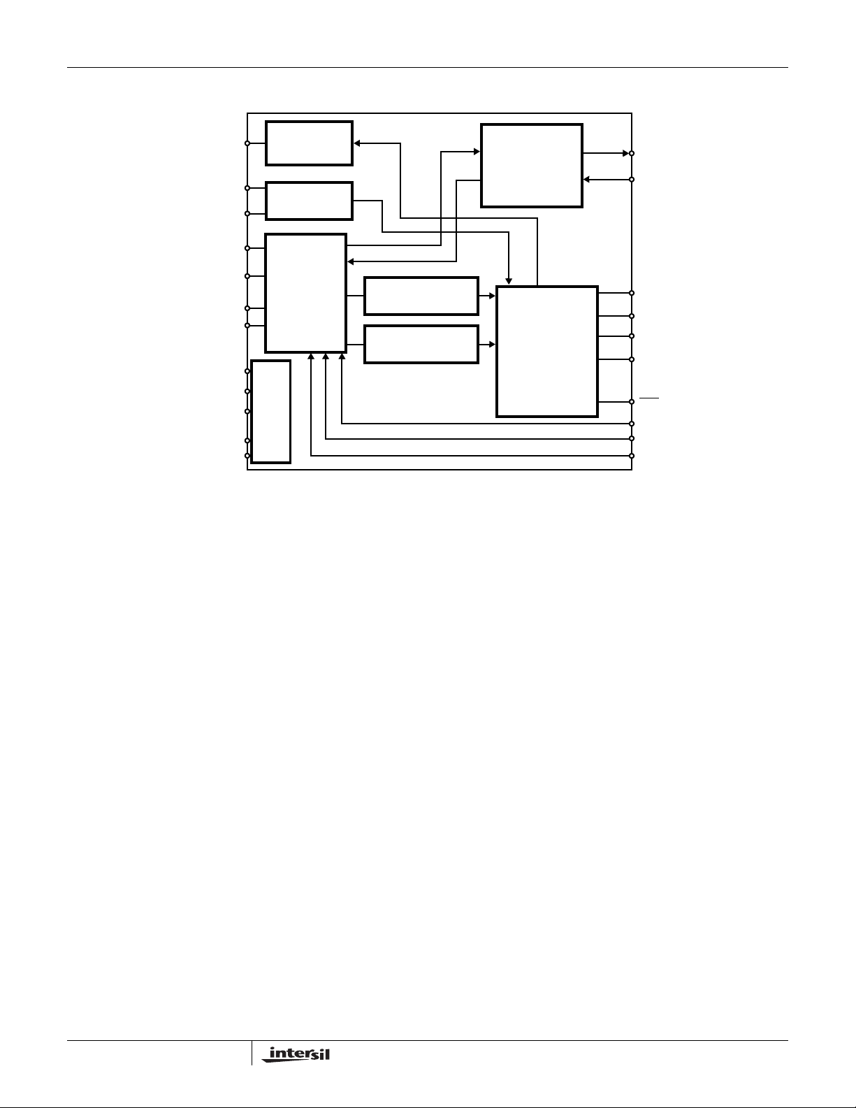
Block Diagram
www.BDTIC.com/Intersil
HC5526
RINGRLY
DT
DR
TIP
RING
HPT
HPR
V
BAT
V
V
AGND
BGND
CC
EE
RING RELAY
RING TRIP
DETECTOR
INTERFACE
BIAS
DRIVER
2-WIRE
LOOP CURRENT
DETECTOR
GROUND KEY
DETECTOR
4-WIRE
INTERFACE
VF SIGNAL
PATH
DIGITAL
MULTIPLEXER
V
TX
RSN
E0
E1
C1
C2
DET
R
D
R
DC
RSG
3
Page 4
HC5526
www.BDTIC.com/Intersil
Absolute Maximum Ratings Thermal Information
Operating Temperature Range . . . . . . . . . . . . . . . . -40oC to 110oC
Power Supply (-40
Supply Voltage V
Supply Voltage V
Supply Voltage V
Ground
o
C ≤ TA ≤ 85oC)
to GND . . . . . . . . . . . . . . . . . . . . 0.5V to 7V
CC
to GND. . . . . . . . . . . . . . . . . . . . . -7V to 0.5V
EE
to GND. . . . . . . . . . . . . . . . . . .-70V to 0.5V
BAT
Voltage between AGND and BGND . . . . . . . . . . . . . -0.3V to 0.3V
Relay Driver
Ring Relay Supply Voltage . . . . . . . . . . . . . . . . . . . . . 0V to 20V
Ring Relay Current. . . . . . . . . . . . . . . . . . . . . . . . . . . . . . . . 50mA
Ring Trip Comparator
Input Voltage . . . . . . . . . . . . . . . . . . . . . . . . . . . . . . . . V
BAT
to 0V
Input Current . . . . . . . . . . . . . . . . . . . . . . . . . . . . . . -5mA to 5mA
Digital Inputs, Outputs (C1, C2, E0, E1, DET
Input Voltage . . . . . . . . . . . . . . . . . . . . . . . . . . . . . . . . .0V to V
Output Voltage (DET Not Active) . . . . . . . . . . . . . . . . . 0V to V
Output Current (DET). . . . . . . . . . . . . . . . . . . . . . . . . . . . . . . 5mA
Tipx and Ringx Terminals (-40
o
C ≤ TA ≤ 85oC)
Tipx or Ringx V oltag e, Contin uous (Referenced to GND) V
Tipx or Ringx, Pulse < 10ms, T
Tipx or Ringx, Pulse < 10µs, T
Tipx or Ringx, Pulse < 250ns, T
Tipx or Ringx Current. . . . . . . . . . . . . . . . . . . . . . . . . . . . . . 70mA
REP
REP
REP
)
> 10s . . . . . .V
> 10s . . . . V
> 10s. . . . V
-20V to 5V
BAT
-40V to 10V
BAT
-70V to 15V
BAT
BAT
CC
CC
to 2V
ESD Rating . . . . . . . . . . . . . . . . . . . . . . . . . . . . . . . . . . . . . . . 500V
Thermal Resistance (Typical, Note 1)
28 Lead PLCC Package. . . . . . . . . . . . . . . . . . . . . . 53
Continuous Dissipation at 70
28 Lead PLCC Package. . . . . . . . . . . . . . . . . . . . . . . . . . . . .1.5W
Package Power Dissipation at 70
28 Lead PLCC Package . . . . . . . . . . . . . . . . . . . . . . . . . . . . . 4W
Derate above . . . . . . . . . . . . . . . . . . . . . . . . . . . . . . . . . . . . . . 70
PLCC Package. . . . . . . . . . . . . . . . . . . . . . . . . . . . . . 18.8mW/
Maximum Junction Temperature Range . . . . . . . . . -40
Maximum Storage Temperature Range. . . . . . . . . . -65
Maximum Lead Temperature (Soldering 10s). . . . . . . . . . . . . 300
(PLCC - Lead Tips Only)
Die Characteristics
Gate Count . . . . . . . . . . . . . . . . . . . . . . 543 Transistors, 51 Diodes
o
C
o
C, t < 100ms, t
REP
θ
JA
> 1s
o
C to 150oC
o
C to 150oC
(oC/W)
o
o
o
C
C
C
CAUTION: Stresses above those listed in “Absolute Maximum Ratings” may cause permanent damage to the device. This is a stress only rating and operation of the
device at these or any other conditions above those indicated in the operational sections of this specification is not implied.
NOTE:
1. θ
is measured with the component mounted on an evaluation PC board in free air.
JA
Typical Ope rating Conditions
These represent the conditions under which the part was developed and are suggested as guidelines.
PARAMETER CONDITIONS MIN TYP MAX UNITS
o
DC2
R
600kΩ
R
300kΩ
C
= 41.2kΩ,
PEAK
T
RX
R
Case Temperature -40 - 100
with Respect to AGND 0oC to 70oC 4.75 - 5.25 V
V
CC
V
with Respect to AGND 0oC to 70oC -5.25 - -4.75 V
EE
with Respect to BGND 0oC to 70oC -58 - -24 V
V
BAT
Electrical Specifications T
= 0oC to 70oC, VCC = 5V ±5%, V
A
= 39kΩ, RSG = ∞, RF1 = RF2 = 0Ω, CHP = 10nF, CDC = 1.5µF, ZL = 600Ω.
R
D
= -5V ±5%, V
EE
= -28V, AGND = BGND = 0V, R
BAT
DC1
= R
PARAMETER CONDITIONS MIN TYP MAX UNITS
Overload Level 1% THD, Z
= 600Ω, (Note 2, Figure 1) 3.1 - - V
L
Longitudinal Impedance (Tip/Ring) 0 < f < 100Hz (Note 3, Figure 2) - 20 35 Ω/Wire
R
600Ω
I
DCMET
23mA
A
300Ω
300Ω
T
A
R
LZT = VT/A
1V
RMS
V
TIP
27
L
V
TRO
RING28RSN
TX
19
R
T
600kΩ
E
R
RX
16
300kΩ
RX
0 < f < 100Hz
E
L
2.16µF
C
V
T
V
R
TIP
27
RING28RSN
T
V
TX
19
16
LZR = VR/A
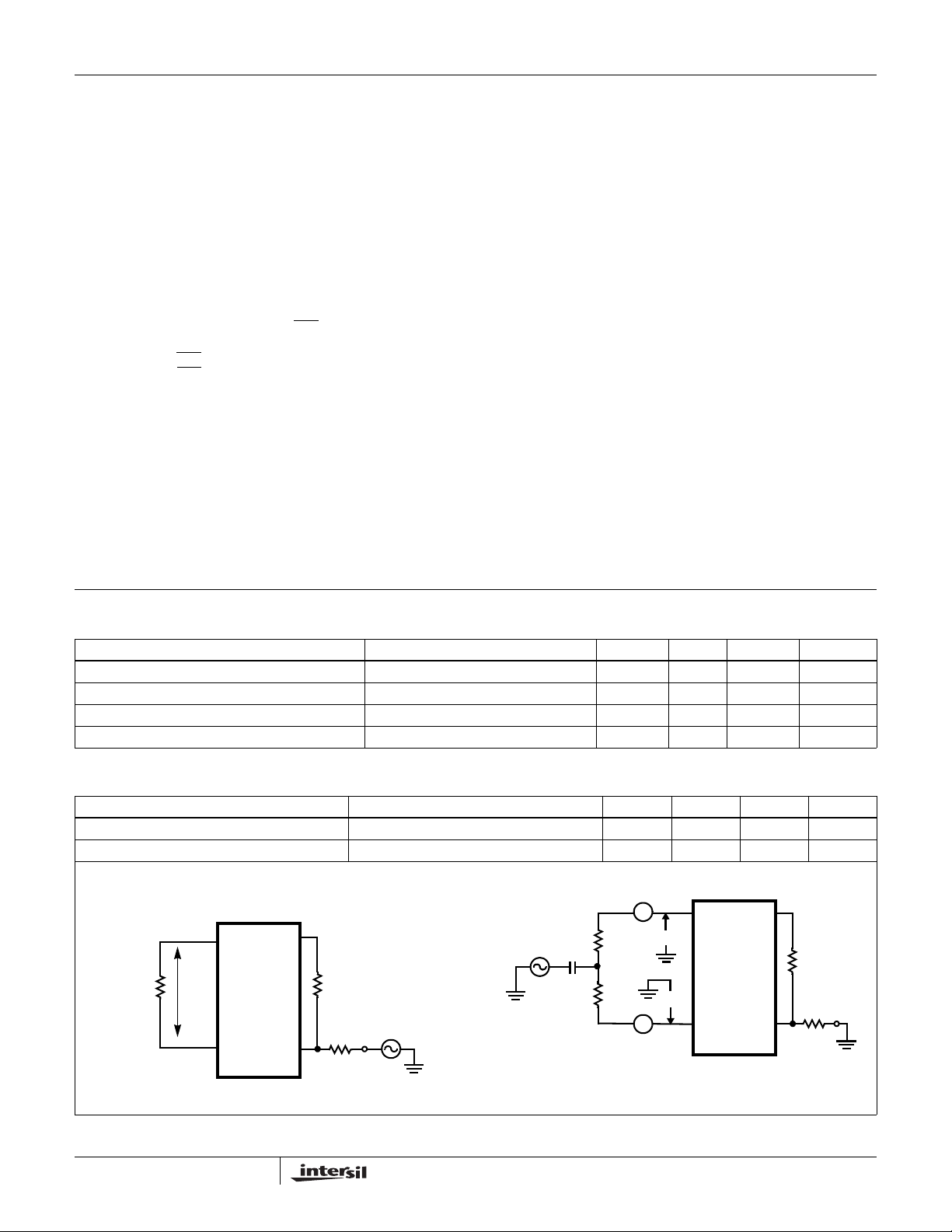
FIGURE 1. OVERLOAD LEVEL (TWO-WIRE PORT)
FIGURE 2. LONGITUDINAL IMPEDANCE
4
Page 5
HC5526
www.BDTIC.com/Intersil
Electrical Specifications T
= 0oC to 70oC, VCC = 5V ±5%, V
A
= 39kΩ, RSG = ∞, RF1 = RF2 = 0Ω, CHP = 10nF, CDC = 1.5µF, ZL = 600Ω. (Continued)
R
D
= -5V ±5%, V
EE
= -28V, AGND = BGND = 0V, R
BAT
DC1
= R
DC2
= 41.2kΩ,
PARAMETER CONDITIONS MIN TYP MAX UNITS
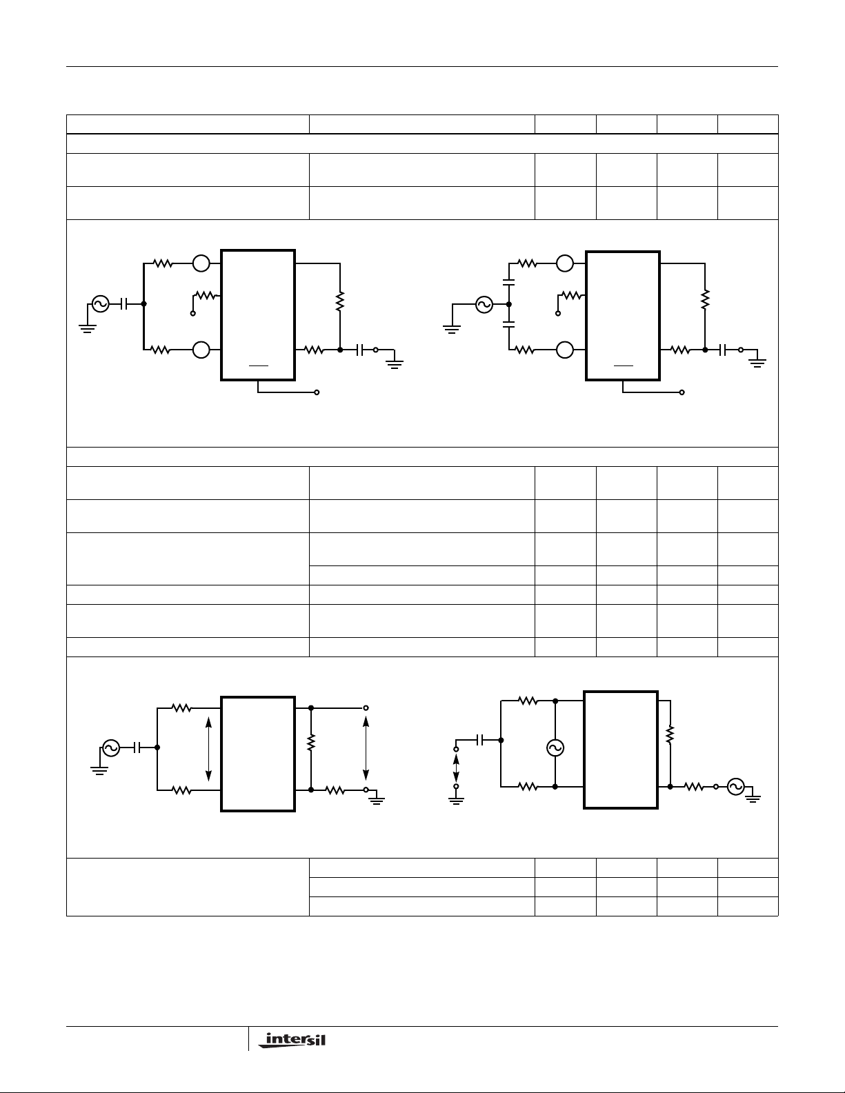
LONGITUDINAL CURRENT LIMIT (TIP/RING)
Off-Hook (Active) No False Detections (Loop Current),
--20mA
LB > 45dB (Note 4, Figure 3A)
On-Hook (Standby), R
368Ω
E
C
L
2.16µF
368Ω
= ∞ No False Detections (Loop Current)
L
A
39kΩ
-5V
A
TIP
27
R
RING28R
RSN
D
DET
(Note 5, Figure 3B)
16
R
DC2
DC
14
41.2kΩ
R
DC1
41.2kΩ
C
DC
1.5µF
E
L
368Ω
C2.16µF
C2.16µF
368Ω
--5mA
A
39kΩ
-5V
A
TIP
27
R
RING
28
RSN
16
R
D
R
DC2
R
DC
41.2kΩ
14
DET
DC1
41.2kΩ
C
DC
1.5µF
FIGURE 3A. OFF-HOOK FIGURE 3B. ON-HOOK
FIGURE 3. LONGITUDINAL CURRENT LIMIT
OFF-HOOK LONGITUDINAL BALANCE
Longitudinal to Metallic IEEE 455 - 1985, R
, RLT = 368Ω,
LR
53 60 - dB
0.2kHz < f < 4.0kHz (Note 6, Figure 4)
Longitudinal to Metallic R
, RLT = 300Ω, 0.2kHz < f < 4.0kHz
LR
53 60 - dB
(Note 6, Figure 4)
Metallic to Longitudinal FCC Part 68, Para 68.310
50 55 - dB
0.2kHz < f < 1.0kHz
1.0kHz < f < 4.0kHz (Note 7) 50 55 - dB
Longitudinal to 4-Wire 0.2kHz < f < 4.0kHz (Note 8, Figure 4) 53 60 - dB
Metallic to Longitudinal R
, RLT = 300Ω, 0.2kHz < f < 4.0kHz
LR
(Note 9, Figure 5)
50 55 - dB
4-Wire to Longitudinal 0.2kHz < f < 4.0kHz (Note 10, Figure 5) 50 55 - dB
PEAK
Wire
PEAK
Wire
/
/
R
E
L
C
2.16µF
LT
R
LR
TIP
27
V
TR
RING
28
V
RSN
TX
19
16
FIGURE 4. LONGITUDINAL TO METALLIC AND
LONGITUDINAL TO 4-WIRE BALANCE
2-Wire Return Loss
= 20nF
C
HP
R
T
600kΩ
R
RX
300kΩ
V
TX
2.16µF
V
L
C
FIGURE 5. METALLIC TO LONGITUDINAL AND 4-WIRE TO
0.2kHz to 0.5kHz (Note 11, Figure 6) 25 - - dB
0.5kHz to 1.0kHz (Note 11, Figure 6) 27 - - dB
R
300Ω
R
300Ω
LONGITUDINAL BALANCE
1.0kHz to 3.4kHz (Note 11, Figure 6) 23 - - dB
5
LT
LR
E
TR
TIP
27
RING28RSN
V
TX
19
16
R
T
600kΩ
R
RX
300kΩ
E
RX
Page 6

HC5526
www.BDTIC.com/Intersil
Electrical Specifications T
= 0oC to 70oC, VCC = 5V ±5%, V
A
= 39kΩ, RSG = ∞, RF1 = RF2 = 0Ω, CHP = 10nF, CDC = 1.5µF, ZL = 600Ω. (Continued)
R
D
= -5V ±5%, V
EE
= -28V, AGND = BGND = 0V, R
BAT
DC1
= R
DC2
= 41.2kΩ,
PARAMETER CONDITIONS MIN TYP MAX UNITS
TIP IDLE VOLTAGE
Active, I
Standby, I
= 0 --4-V
L
= 0 -<0 - V
L
RING IDLE VOLTAGE
Active, I
Standby, I
4-WIRE TRANSMIT PORT (V
Overload Level Z
= 0 --24- V
L
= 0 ->-28- V
L
)
TX
> 20kΩ, 1% THD (Note 12, Figure 7) 3.1 - - V
L
Output Offset Voltage EG = 0, ZL = ∞ (Note 13, Figure 7) -60 - 60 mV
Output Impedance (Guaranteed by Design) 0.2kHz < f < 03.4kHz - 5 20 W
2- to 4-Wire (Metallic to V
R
V
S
R
R
LR
) Voltage Gain 0.3kHz < f < 03.4kHz (Note 14, Figure 7) 0.98 1.0 1.02 V/V
TX
R
600Ω
E
2.16µF
L
C
I
DCMET
23mA
G
V
TR
TIP27V
19
RING28RSN
16
TX
R
T
600kΩ
R
RX
300kΩ
Z
D
TIP
27
V
M
Z
IN
RING28RSN
V
TX
19
R
T
600kΩ
R
RX
16
300kΩ
V
V
TXO
TX
PEAK
Z
L
FIGURE 6. TWO-WIRE RETURN LOSS FIGURE 7. OVERLO AD LEVEL (4-WIRE TRANSMIT PORT),
OUTPUT OFFSET VOLTAGE, 2-WIRE TO 4-WIRE
VOLTAGE GAIN AND HARMONIC DISTORTION
4-WIRE RECEIVE PORT (RSN)
DC Voltage I
R
Sum Node Impedance (Guaranteed by
X
Design)
= 0mA - 0 - V
RSN
0.3kHz < f < 3.4kHz - - 20 W
Current Gain-RSN to Metallic 0.3kHz < f < 3.4kHz (Note 15, Figure 8) 980 1000 1020 Ratio
FREQUENCY RESPONSE (OFF-HOOK)
2-Wire to 4-Wire 0dBm at 1.0kHz, E
0.3kHz < f < 3.4kHz (Note 16, Figure 9)
4-Wire to 2-Wire 0dBm at 1.0kHz, E
0.3kHz < f < 3.4kHz (Note 17, Figure 9)
4-Wire to 4-Wire 0dBm at 1.0kHz, E
0.3kHz < f < 3.4kHz (Note 18, Figure 9)
RX
G
G
= 0V,
= 0V,
= 0V,
-0.2 - 0.2 dB
-0.2 - 0.2 dB
-0.2 - 0.2 dB
INSERTION LOSS
2-Wire to 4-Wire 0dBm, 1kHz (Note 19, Figure 9) -0.2 - 0.2 dB
4-Wire to 2-Wire 0dBm, 1kHz (Note 20, Figure 9) -0.2 - 0.2 dB
GAIN TRACKING (Ref = -10dBm, at 1.0kHz)
2-Wire to 4-Wire -40dBm to +3dBm (Note 21, Figure 9) -0.1 - 0.1 dB
2-Wire to 4-Wire -55dBm to -40dBm (Note 21, Figure 9) - ±0.03 - dB
4-Wire to 2-Wire -40dBm to +3dBm (Note 22, Figure 9) -0.1 - 0.1 dB
6
Page 7

HC5526
www.BDTIC.com/Intersil
Electrical Specifications T
= 0oC to 70oC, VCC = 5V ±5%, V
A
= 39kΩ, RSG = ∞, RF1 = RF2 = 0Ω, CHP = 10nF, CDC = 1.5µF, ZL = 600Ω. (Continued)
R
D
= -5V ±5%, V
EE
= -28V, AGND = BGND = 0V, R
BAT
DC1
= R
DC2
= 41.2kΩ,
PARAMETER CONDITIONS MIN TYP MAX UNITS
4-Wire to 2-Wire -55dBm to -40dBm (Note 22, Figure 9) - ±0.03 - dB
GRX = ((V
Where: V
and V
- V
)(300k))/(-3)(600)
TR2
is the Tip to Ring Voltage with V
is the Tip to Ring Voltage with V
TIP
27
V
TR
RING28R
R
600Ω
TR1
TR1
TR2
L
RSN
16
DC
14
R
RX
300kΩ
R
DC2
41.2kΩ
RSN
RSN
= 0V
= -3V
R
DC1
41.2kΩ
V
V
C
DC
1.5µF
RSN
RSN
= 0V
= -3V
R
600Ω
E
G
1/ωC << RL
C
TIP27V
L
I
DCMET
V
TR
RING28RSN
TX
19
R
T
600kΩ
R
RX
16
300kΩ
V
TX
E
RX
FIGURE 8. CURRENT GAIN-RSN TO METALLIC FIGURE 9. FREQUENCY RESPONSE, INSERTION LOSS, GAIN
TRACKING AND HARMONIC DISTORTION
NOISE
Idle Channel Noise at 2-Wire C-Message Weighting (Note 23, Figure 10) - 10 - dBrnC
Idle Channel Noise at 4-Wire C-Message Weighting (Note 24, Figure 10) - 10 - dBrnC
HARMONIC DISTORTION
2-Wire to 4-Wire 0dBm, 1kHz (Note 25, Figure 7) - -65 -54 dB
4-Wire to 2-Wire 0dBm, 0.3kHz to 3.4kHz (Note 26,
--65-54dB
Figure 9)
BATTERY FEED CHARACTERISTICS
Constant Loop Current Tolerance
R
DCX
= 41.2kΩ
Loop Current Tolerance (Standby) I
Open Circuit Voltage (V
TIP
- V
)0
RING
I
= 2500/(R
L
o
C to 70oC (Note 27)
0
= (V
L
BAT
o
C to 70oC (Note 28)
0
o
C to 70oC, (Active) 14 - 20 V
+ R
DC1
DC2
-3)/(RL +1800),
),
0.9I
0.8I
L
L
I
L
I
L
1.1I
1.2I
L
L
mA
mA
LOOP CURRENT DETECTOR
On-Hook to Off-Hook R
Off-Hook to On-Hook R
Loop Current Hysteresis R
= 39kΩ, 0oC to 70oC 372/R
D
= 39kΩ, 0oC to 70oC 325/R
D
= 39kΩ, 0oC to 70oC 25/R
D
465/R
D
405/R
D
60/R
D
558/R
D
485/R
D
95/R
D
D
mA
D
mA
D
mA
GROUND KEY DETECTOR
Tip/Ring Current Difference - Trigger (Note 29, Figure 11) 8 12 17 mA
Tip/Ring Current Difference - Reset (Note 29, Figure 11) 3 7 12 mA
7
Page 8

HC5526
www.BDTIC.com/Intersil
Electrical Specifications T
= 0oC to 70oC, VCC = 5V ±5%, V
A
= 39kΩ, RSG = ∞, RF1 = RF2 = 0Ω, CHP = 10nF, CDC = 1.5µF, ZL = 600Ω. (Continued)
R
D
= -5V ±5%, V
EE
= -28V, AGND = BGND = 0V, R
BAT
DC1
= R
DC2
= 41.2kΩ,
PARAMETER CONDITIONS MIN TYP MAX UNITS
Hysteresis (Note 29, Figure 11) 0 5 9 mA
R
600Ω
TIP27V
L
V
TR V
RING28RSN
TX
19
16
R
T
600kΩ
R
RX
300kΩ
TIP
27
TX
RING28R
DET
RSN
16
DC
14
R
DC2
41.2kΩ
E1 = C1 = 0, C2 = 1
R
DC1
41.2kΩ
C
DC
1.5µF
FIGURE 10. IDLE CHANNEL NOISE FIGURE 11. GROUND KEY DETECT
RING TRIP DETECTOR (DT, DR)
Offset Voltage Source Res = 0 -20 - 20 mV
Input Bias Current Source Res = 0 -500 - 500 nA
Input Common-Mode Range Source Res = 0 V
+1 - 0 V
BAT
Input Resistance Source Res = 0, Balanced 3 - - MΩ
RING RELAY DRIVER
V
at 25mA IOL = 25mA - 1.0 1.5 V
SAT
Off-State Leakage Current V
= 12V - - 10 µA
OH
DIGITAL INPUTS (E0, E1, C1, C2)
Input Low Voltage, V
Input High Voltage, V
Input Low Current, I
Input Low Current, I
IL
IH
: C1, C2 VIL = 0.4V -200 - - µA
IL
: E0, E1 VIL = 0.4V -100 - - µA
IL
Input High Current V
DETECTOR OUTPUT (DET
Output Low Voltage, V
Output High Voltage, V
)
OL
OH
= 2.4V - - 40 µA
IH
IOL = 2mA - - 0.45 V
IOH = 100µA2.7--V
0-0.8V
2-VCCV
Internal Pull-Up Resistor 10 15 20 k
POWER DISSIPATION
Open Circuit State C1 = C2 = 0 - - 23 mW
On-Hook, Standby C1 = C2 = 1 - - 30 mW
On-Hook, Active C1 = 0, C2 = 1, R
Off-Hook, Active R
= 0Ω --1.1W
L
= 300Ω - - 0.75 W
R
L
= 600Ω --0.5W
R
L
= High Impedance - - 150 mW
L
TEMPERATURE GUARD
Thermal Shutdown 150 - 180
Ω
o
C
8
Page 9

HC5526
www.BDTIC.com/Intersil
Electrical Specifications T
PARAMETER CONDITIONS MIN TYP MAX UNITS
SUPPLY CURRENTS (V
, On-Hook Open Circuit State (C1, 2 = 0, 0) - - 1.5 mA
I
CC
I
, On-Hook Open Circuit State (C1, 2 = 0, 0) - - 0.8 mA
EE
I
, On-Hook Open Circuit State (C1, 2 = 0, 0) - - 0.4 mA
BAT
PSRR
V
to 2 or 4-Wire Port (Note 30, Figure 12) - 40 - dB
CC
to 2 or 4-Wire Port (Note 30, Figure 12) - 40 - dB
V
EE
to 2 or 4-Wire Port (Note 30, Figure 12) - 40 - dB
V
BAT
BAT
= 0oC to 70oC, VCC = 5V ±5%, V
A
= 39kΩ, RSG = ∞, RF1 = RF2 = 0Ω, CHP = 10nF, CDC = 1.5µF, ZL = 600Ω. (Continued)
R
D
= -28V)
Standby State (C1, 2 = 1, 1) - - 1.7 mA
Active State (C1, 2 = 0,1) - - 5.5 mA
Standby State (C1, 2 = 1, 1) - - 0.8 mA
Active State (C1, 2 = 0, 1) - - 2.2 mA
Standby State (C1, 2 = 1, 1) - - 0.6 mA
Active State (C1, 2 = 0, 1) - - 3.9 mA
-48V SUPPLY
5V SUPPLY
-5V SUPPLY
100mV
= -5V ±5%, V
EE
, 50Hz TO 4kHz
RMS
= -28V, AGND = BGND = 0V, R
BAT
DC1
= R
DC2
= 41.2kΩ,
R
L
600Ω
TIP27V
RING28RSN
FIGURE 12. POWER SUPPLY REJECTION RATIO
TX
19
16
Circuit Operation and Design Information
The HC5526 is a current feed voltage sense Subscriber Line
Interface Circuit (SLIC). This means that for short loop
applications the SLIC provides a programmed constant
current to the tip and ring terminals while sensing the tip to
ring voltage.
The following discussion separates the SLIC’s operation into
its DC and AC paths, then follows up with additional circuit
and design information.
Constant Loop Current (DC) Path
SLIC in the Active Mode
The DC path establishes a constant loop current that flows
out of tip and into the ring terminal. The loop current is
programmed by resistors R
the R
the voltage across R
pin (Figure 13). The RDC voltage is determined by
DC
in the saturation guard circuit. Under
1
constant current feed conditions, the voltage drop across R
DC1
, R
and the voltage on
DC2
R
T
600kΩ
R
300kΩ
RX
sets the R
PSRR = 20 log (V
V
TX
DC
flows through R
establishes a current (I
+R
). This current is then multiplied by 1000, in the loop
DC2
voltage to -2.5V. This occurs when current
into the current source I2. The RDC voltage
1
)
TX/VIN
) that is equal to V
RSN
RDC
/(R
DC1
current circuit, to become the tip and ring loop currents.
For the purpose of the following discussion, the saturation
guard voltage is defined as the maximum tip to ring voltage
at which the SLIC can provide a constant current for a given
battery and overhead voltage.
1
9
Page 10

I
www.BDTIC.com/Intersil
RING
I
TIP
TIP
RING
HC5526
I
TIP
HC5526
+
-
I
RING
-
+
FIGURE 13. DC LOOP CURRENT
LOOP CURRENT
CIRCUIT
SATURATION GUARD
CIRCUIT
A
1
I
1
-5V
V
TX
I
RSN
-
A
2
I
2
-5V
+
R
1
-
+
RSN
R
DC
-2.5V
R
SG
-5V
R
RX
R
DC1
C
R
DC2
R
SG
DC
For loop resistances that result in a tip to ring voltage less than
the saturation guard voltage the loop current is defined as:
I
L
+
R
DC1RDC2
1000×= (EQ. 1)
2.5V
------------------------------------- -
where: IL = Constant loop current.
R
and R
DC1
Capacitor CDC between R
= Loop current programming resistors.
DC2
DC1
and R
removes the VF
DC2
signals from the battery feed control loop. The value of CDC
is determined by Equation 2:
1
T
---------------
C
DC
×=
R
DC1
---------------+
R
1
DC2
(EQ. 2)
where T = 30ms.
The minimum C
value is obtained if R
DC
DC1
= R
DC2
.
Figure 14 illustrates the relationship between the tip to ring
voltage and the loop resistance. For a 0Ω loop resistance both
tip and ring are at V
/2. As the loop resistance increases, so
BAT
does the voltage differential between tip and ring. When this
differential voltage becomes equal to the saturation guard
voltage, the operation of the SLIC’ s loop f eed changes from a
constant current feed to a resistive feed. The loop current in the
resistive feed region is no longer constant but v aries as a
function of the loop resistance.
V
= -48V, IL = 23mA, RSG = 21.4kΩ
BAT
RESISTIVE FEED
LOOP RESISTANCE (Ω)
FIGURE 14. VTR vs R
REGION
L
V
TIP
V
RING
∞
TIP TO RING VOLTAGE (V)
0
-10
-20
-30
-40
-50
SATURATION
GUARD V OLTAGE
CONSTANT CURRENT
FEED REGION
SATURATION
GUARD V OLTAGE
01.2K
Figure 15 shows the relationship between the saturation guard
voltage, the loop current and the loop resistance. Notice from
Figure 15 that for a loop resistance <1.2kΩ (R
= 21.4kΩ) the
SG
SLIC is operating in the constant current feed region and for
resistances >1.2kΩ the SLIC is operating in the resistive feed
region. Operation in the resistive feed region allows long loop
and off-hook transmission by keeping the tip and ring voltages
off the rails. Operation in this region is transparent to the
customer.
50
40
30
20
10
TIP TO RING VOLTAGE (V)
0
0
R
L
R
100kΩ
L
V
= -48V, RSG = 21.4kΩ
BAT
V
= -24V, RSG = ∞
BAT
RESISTIVE FEED
REGION
10 20
LOOP CURRENT (mA)
4kΩ
1.5kΩ
FIGURE 15. VTR vs IL and R
2kΩ
700Ω <400Ω
CONST ANT CURRENT
FEED REGION
SATURATION GUARD
VOLTAGE, V
SATURATION GUARD
VOLTAGE, V
30
<1.2kΩ
R
RSG
R
RSG
L
= 38V
TR
= 13V
TR
= 21.4kΩ100kΩ
= ∞Ω
The Saturation Guard circuit (Figure 13) monitors the tip to
ring voltage via the transconductance amplifier A
. A1
1
generates a current that is proportional to the tip to ring
voltage difference. I
is internally set to sink all of A1’s
1
current until the tip to ring voltage exceeds 12.5V. When the
tip to ring voltage exceeds 12.5V (with no R
supplies more current than I
A
amplifies its input current by a factor of 12 and the current
2
through R
output current from A
voltage across R
becomes the difference between I2 and the
1
2
decreases and the output voltage on RDC
1
can sink. When this happens
1
. As the current from A2 increases, the
resistor) A1
SG
decreases. This results in a corresponding decrease in the
loop current. The R
pin provides the ability to increase the
SG
saturation guard reference voltage beyond 12.5V. Equation 3
10
Page 11

HC5526
www.BDTIC.com/Intersil
gives the relationship between the R
resistor value and
SG
the programmable saturation guard reference voltage:
V
SGREF
12.5
510•
------------------+=
5
R
SG
(EQ. 3)
where:
V
R
= Saturation Guard reference voltage, and,
SGREF
= Saturation Guard programming resistor.
SG
When the Saturation guard reference voltage is exceeded,
the tip to ring voltage is calculated using Equation 4:
V
TRRL
16.66 5 105• RSG⁄+
----------------------------------------------------------------------
×=
R
LRDC1RDC2
+()600⁄+
(EQ. 4)
where:
V
= Voltage differential between tip and ring, and ,
TR
= Loop resistance.
R
L
For on-hook transmission R
5
•
510
16.66
V
TR
------------------+=
R
SG
= ∞, Equation 4 reduces to:
L
(EQ. 5)
The value of RSG should be calculated to allow maximum
loop length operation. This requires that the saturation guard
reference voltage be set as high as possible without clipping
the incoming or outgoing VF signal. A voltage margin of -4V
on tip and -4V on ring, for a total of -8V margin, is
recommended as a general guideline. The value of R
SG
is
calculated using Equation 6:
5
510
--------------------------------------------------------------------------------------------------------------------------------------------------=
R
SG
–()1
V
BATVMARGIN
•
+()
R
DC1RDC2
------------------------------------------+
600R
L
16.66V–×
(EQ. 6)
where:
= Battery voltage, and
V
BAT
V
MARGIN
overload level of 3.1V
For on-hook transmission R
R
SG
= Recommended value of -8V to allow a maximum
.
PEAK
= ∞, Equation 6 reduces to:
L
510
----------------------------------------------------------------------------=
V
BATVMARGIN
•
5
16.66V––
(EQ. 7)
SLIC in the Standby Mode
Overall system pow er is sav ed by configuring the SLIC in the
standby state when not in use. In the standby state the tip
and ring amplifiers are disabled and internal resistors are
connected between tip to ground and ring to V
connection enables a loop current to flow when the phone
goes off-hook. The loop current detector then detects this
current and the SLIC is configured in the active mode for
voice transmission. The loop current in standby state is
calculated as follows:
V
3V–
BAT
--------------------------------
≈
I
L
1800Ω+
R
L
BAT
. This
(EQ. 8)
where:
= Loop current in the standby state,
I
L
= Loop resistance, and
R
L
V
= Battery voltage.
BAT
(AC) Transmission Path
SLIC in the Active Mode
Figure 16 shows a simplified AC transmission model. Circuit
analysis yields the following design equations:
V
TRVTXIM2RF
V
V
TX
RX
---------- -
-----------+
Z
Z
T
RX
V
TREGIMZL
•+=
I
M
------------ -=
1000
•–=
(EQ. 9)
(EQ. 10)
(EQ. 11)
where:
= Is the AC metallic voltage between tip and ring,
V
TR
including the voltage drop across the fuse resistors R
V
= Is the AC metallic voltage. Either at the ground
TX
,
F
referenced 4-wire side or the SLIC tip and ring terminals,
IM = Is the AC metallic current,
R
= Is a fuse resistor,
F
Z
= Is used to set the SLIC’s 2-wire impedance,
T
VRX = Is the analog ground referenced receive signal,
Z
= Is used to set the 4-wire to 2-wire gain,
RX
E
= Is the AC open circuit voltage, and
G
ZL = Is the line impedance.
(AC) 2-Wire Impedance
The AC 2-wire impedance (ZTR) is the impedance looking
into the SLIC, including the fuse resistors, and is calculated
as follows:
Let V
Z
Substituting in Equation 9 for V
Substituting in Equation 12 for V
= 0. Then from Equation 10:
RX
I
M
------------ -
V
TXZT
TR
Z
TR
Z
TR
Z
TR
•=
1000
is defined as:
V
TR
-----------=
I
M
V
2R
TX
---------- -
-----------------------+=
I
M
Z
T
+=
------------ - 2R
1000
•
FIM
I
M
F
TR
TX
(EQ. 12)
(EQ. 13)
:
(EQ. 14)
:
(EQ. 15)
11
Page 12

7
HC5526
www.BDTIC.com/Intersil
I
TIP
Z
L
Z
+
V
TR
-
TR
+
E
G
-
RING
M
R
F
+
+
V
TX
-
I
M
R
F
-
HC5526
A = 250
V
TX
1
Z
T
A = 4
A = 250
RSN
1000
I
M
+
V
TX
-
Z
RX
+
V
RX
-
FIGURE 16. SIMPLIFIED AC TRANSMISSION CIRCUIT
Therefore:
1000 ZTR2RF–()•=
Z
T
(EQ. 16)
Equation 16 can now be used to match the SLIC’s
impedance to any known line impedance (ZTR).
Example:
Calculate ZT to make ZTR = 600Ω in series with 2.16µF.
RF = 20Ω.
Z
T
= 560kΩ in series with 2.16nF.
Z
T
1000 600
•=
1
----------------------------------------- 220•–+
jω 2.16• 10
•
6–
(AC) 2-Wire to 4-Wire Gain
The 2-wire to 4-wire gain is equal to VTX/ VTR.
From Equations 9 and 10 with V
24–
V
TX
-----------
V
TR
------------------------------------------==
Z
T
Z
T
1000⁄ 2RF+
1000⁄
RX
= 0:
(EQ. 1
For applications where the 2-wire impedance (Z
V
A
42–
TR
-----------
V
RX
Z
T
-----------–
•==
Z
RX
Z
Z
T
++
L
FZL
--------------------------------------------
------------ - 2R
1000
Equation 15) is chosen to equal the line impedance (Z
expression for A
A
42–
Z
-----------–
Z
RX
1
T
-- -
•=
2
simplifies to:
4-2
TR
,
(EQ. 18)
L
(EQ. 19)
), the
(AC) 4-Wire to 4-Wire Gain
The 4-wire to 4-wire gain is equal to VTX/VRX.
2RF+
G
FZL
= 0:
(EQ. 20)
From Equations 9, 10 and 11 with E
V
TX
44–
-----------
V
RX
A
Z
-----------–
Z
RX
Z
T
L
--------------------------------------------
•==
Z
T
------------ - 2R
1000
++
Transhybrid Circuit
The purpose of the transhybrid circuit is to remove the receive
signal (V
an echo on the transmit side. This is accomplished by using an
external op amp (usually part of the CODEC) and by the
inversion of the signal from the 4-wire receive port (RSN) to the
4-wire transmit port (V
circuit. The input signal will be subtracted from the output signal
if I
equals I2. Node analysis yields the following equation:
1
V
TX
-----------
R
TX
) from the transmit signal (VTX), thereby preventing
RX
). Figure 17 shows the transhybrid
TX
V
RX
-----------+ 0=
Z
B
(EQ. 21)
(AC) 4-Wire to 2-Wire Gain
The 4-wire to 2-wire gain is equal to VTR/VRX.
From Equations 9, 10 and 11 with E
G
= 0:
The value of Z
•=
R–
Z
B
TX
Where V
RX/VTX
V
-----------
V
12
is then:
B
RX
TX
equals 1/ A
4-4
(EQ. 22)
.
Page 13

HC5526
www.BDTIC.com/Intersil
Therefore:
Z
T
------------ - 2R
++
1000
--------------------------------------------
•=
2RF+
Z
L
FZL
(EQ. 23)
ZBR
TX
Z
RX
-----------
•
Z
T
Example:
Given: RTX = 20kΩ, ZRX = 280kΩ, ZT = 562kΩ (standard
value), R
The value of Z
HC5526
= 20Ω and ZL = 600Ω.
F
= 18.7kΩ.
B
V
TX
RSN
R
TX
Z
T
Z
RX
R
I
2
I
1
Z
B
FB
-
+
+
V
TX
-
+
V
RX
-
CODEC/
FILTER
FIGURE 17. TRANSHYBRID CIRCUIT
Supervisory Functions
The loop current, ground key and the ring trip detector
outputs are multiplexed to a single logic output pin called
DET. See T ab le 1 to determine the active detector for a given
logic input. For further discussion of the logic circuitry see
section titled “Digital Logic Inputs”.
Before proceeding with an explanation of the loop current
detector, ground ke y detector and later the longitudinal
impedance, it is important to understand the difference between
a “metallic” and “longitudinal” loop currents. Figure 18 illustrates
3 different types of loop current encountered.
Case 1 illustrates the metallic loop current. The definition of
a metallic loop current is when equal currents flow out of tip
and into ring. Loop current is a metallic current.
Cases 2 and 3 illustrate the longitudinal loop current. The
definition of a longitudinal loop current is a common mode
current, that flows either out of or into tip and ring
simultaneously. Longitudinal currents in the on-hook state
result in equal currents flowing through the sense resistors
and R2 (Figure 18). And longitudinal currents in the off-
R
1
hook state result in unequal currents flowing through the
sense resistors R
longitudinal currents flowing away from the SLIC , the current
through R1 is the metallic loop current plus the longitudinal
current; whereas the current through R
current minus the longitudinal current. Longitudinal currents
are generated when the phone line is influenced by magnetic
fields (e.g., power lines).
and R2. Notice that for case 2,
1
is the metallic loop
2
Loop Current Detector
Figure 18 shows a simplified schematic of the loop current
and ground key de tectors . The l oop current detector works b y
sensing the metallic current flowing through resistors R1 and
. This results in a current (IRD) out of the transconductance
R
2
amplifier (gm1) that is equal to the product of gm1 and the
metallic loop current. IRD then flows out the RD pin and
through resistor R
I
TIPIRING
I
----------------------------------- -
RD
The I
600
current results in a voltage drop across RD that is
RD
to VEE. The value of IRD is equal to:
D
–
I
L
--------- -==
300
(EQ. 24)
compared to an internal 1.25V reference voltage. When the
voltage drop across RD exceeds 1.25V, and the logic is
configured for loop current detection, the DET
The hysteresis resistor R
adds an additional voltage
H
pin goes low.
effectively across RD, causing the on-hook to off-hook
threshold to be slightly higher than the off-hook to on-hook
threshold.
Taking into account the hysteresis voltage, the typical value
for the on-hook to off-hook condition is:
of R
D
--------------------------------------------------------------------------=
R
D
I
ON HOO K to OFF– HOOK–
465
(EQ. 25)
Taking into account the hysteresis voltage, the typical value
of R
for the off-hook to on-hook condition is:
D
--------------------------------------------------------------------------=
R
D
I
OFF HOOK to ON– HOOK–
A filter capacitor (C
375
) in parallel with RD will improve the
D
(EQ. 26)
accuracy of the trip point in a noisy environment. The value
of this capacitor is calculated using the following Equation:
T
------- -=
C
D
R
D
(EQ. 27)
where: T = 0.5ms.
Ground Ke y Detector
A simplified schematic of the ground key detector is sho wn in
Figure 18. Ground key, is the process in which the ring
terminal is shorted to ground for the purpose of signaling an
Operator or seizing a phone line (between the Central Office
and a Private Branch Exchange). The Ground K ey detector is
activated when unequal current flow through resistors R
. This results in a current (IGK) out of the transconductance
R
2
and
1
amplifier (gm2) that is equal to the product of gm2 and the
differential (I
internal current source (I
TIP
-I
) loop current. If IGK is less than the
RING
), then diode D1 is on and the output
1
of the ground key comparator is low. If IGK is greater than the
internal current source (I
), then diode D2 is on and the output
1
of the ground key comparator is high. With the outpu t of the
ground key compara tor high, and the logic configured for
ground key detect, the DET
pin goes low . The g round k ey
detector has a built in hysteresis of typical ly 5mA betw een its
trigger and reset values.
Ring Trip Detector
Ring trip detection is accomplished with the internal ring trip
comparator and the exte rnal circuitry shown in Figure 19. The
13
Page 14

HC5526
www.BDTIC.com/Intersil
process of ring trip is initiated when the logic input p ins are in the
following states: E0 = 0, E1 = 1/0, C1 = 1 and C2 = 0. This logic
condition connects the ring trip comparator to the DET output,
and causes the Ringrly pin to energize the ring relay. The ring
relay connects the tip and ring of the phone to the external
circuitry in Figure 19. When the phone is on-hook the DT pin is
CASE 1 CASE 2 CASE 3
I
METALLIC
←
I
LONGITUDINAL
←
I
LONGITUDINAL
→
TIP
RING
R
1
R
2
HC5526
more positive than the DR pin and the DET output is high. For
off-hook conditions DR is more positive than DT and DET goes
low. When DET goes lo w, indicating that the phone has gone
off-hook, the SLIC is commanded by the logic inputs to go into
the active state. In th e activ e st ate, ti p and ring are once a gain
connected to the phone and normal operation e nsues .
gm1(I
METALLIC
+
-
gm
1
gm
2
R
H
-
+
GROUND
KEY
COMPARATOR
CURRENT
COMPARATOR
gm2(I
I
GK
+
-
D
DIGITAL MULTIPLEXER
1
LOOP
- I
TIP
)
RING
D
I
1
R
D
R
H
+
-
+
V
)
2
1.25V
REF
I
RD
C
R
D
D
-
V
EE
-5V
DET
FIGURE 18. LOOP CURRENT AND GROUND KEY DETECTORS
Figure 19 illustrates battery backed unbalanced ring injected
ringing. For tip injected ringing just reverse the leads to the
phone. The ringing source could also be balanced.
NOTE: The DET output will toggle at 20Hz because the DT input is
not completely filtered by C
and determine if the DET
. Software can examine the duty cycle
RT
pin is low for more that half the time, if so
the off-hook condition is indicated.
C
RT
RG
R
4
R
1
R
2
V
BAT
RINGRLY
DT
DR
COMPARATOR
-
+
RING TRIP
HC5526
DET
R
RT
RING
RELAY
TIP
RING
R
3
E
FIGURE 19. RING TRIP CIRCUIT FOR BA TTER Y B ACKED RINGING
Longitudinal Impedance
The feedback loop described in Figure 20(A, B) realizes the
desired longitudinal impedances from tip to ground and from
ring to ground. Nominal longitudinal impedance is resistive
and in the order of 22Ω.
In the presence of longitudinal currents this circuit attenuates
the voltages that would otherwise appear at the tip and ring
terminals, to levels well within the common mode range of
the SLIC. In fact, longitudinal currents may exceed the
programmed DC loop current without disturbing the SLIC’s
VF transmission capabilities.
The function of this circuit is to maintain the tip and ring
voltages symmetrically around V
/2, in the presence of
BAT
longitudinal currents. The differential transconductance
amplifiers G
the required current to maintain VC at V
and GR accomplish this by sourcing or sinking
T
BAT
/2.
When a longitudinal current is injected onto the tip and ring
inputs, the voltage at VC moves from it’s equilibrium value
/2. When VC changes by the amount ∆VC, this change
V
BAT
appears between the input terminals of the differential
transconductance amplifiers G
and G
are the differential currents ∆I1 and ∆I2, which in
R
and GR. The output of GT
T
turn feed the differential inputs of current sources IT and IR
respectively. I
ended and 500 differentially, thus leading to a change in I
that is equal to 500(∆I) and 500(∆I2).
and I
R
and IR have current gains of 250 single
T
T
The circuit shown in Figure 20(B) illustrates the tip side of
the longitudinal network. The advantages of a differential
input current source are: improved noise since the noise due
to current source 2I
is now correlated, power savings due
O
to differential current gain and minimized offset error at the
Operational Amplifier inputs via the two 5kΩ resistors.
Digital Logic Inputs
Table 1 is the logic truth table for the TTL compatible logic
input pins. The HC5526 has two enable inputs pins (E0, E1)
and two control inputs pins (C1, C2).
14
Page 15

8
HC5526
www.BDTIC.com/Intersil
The enable pin E0 is used to enable or disable the DET
output pin. The DET pin is enabled if E0 is at a logic level 0
and disabled if E0 is at a logic level 1.
The enable pin E1 gates the ground key detector to the DET
output with a logic level 0, and gates the loop or ring trip
detector to the DET
output with a logic level 1.
A combination of the control pins C1 and C2 is used to select
1 of the 4 possible operating states. A description of each
operating state and the control logic follow:
I
LONG
I
LONG
I
LONG
I
LONG
∆V
∆V
T
+
R
+
-
-
TIP
R
LARGE
V
C
R
LARGE
RING
HC5526
+
-
I
T
∆I
1
∆I
2
I
R
Open Circuit State (C1 = 0, C2 = 0)
In this state the SLIC is effectively off. All detectors and both
∆I
G
G
∆I
the tip and ring line drive amplifiers are powered down,
presenting a high impedance to the line. Power dissipation is
at a minimum.
TIP CURRENT SOURCE
WITH DIFFERENTIAL INPUTS
1
T
V
/2
BAT
R
2
TIP
V
RING
R
LARGE
C
R
LARGE
20Ω
5kΩ
5kΩ
∆I
1
2I
0
TIP DIFFERENTIAL
TRANSCONDUCTANCE
AMPLIFIER
-
+
∆I
1
V
/2
BAT
G
T
FIGURE 20A. FIGURE 20B.
FIGURE 20. LONGITUDINAL IMPEDANCE NETWORK
Active State (C1 = 0, C2 = 1)
The tip output is capable of sourcing loop current and for
open circuit conditions is about -4V from ground. The ring
output is capable of sinking loop current and for open circuit
conditions is about V
+4V. VF signal transmission is
BAT
normal. The loop current and ground key detectors are both
active, E0 and E1 determine which detector is gated to the
output.
DET
Ringing State (C1 = 1, C2 = 0)
The ring relay driver and the ring trip detector are activated.
Both the tip and ring line drive amplifiers are powered down.
Both tip and ring are disconnected from the line via the
external ring relay.
Standby State (C1 = 1, C2 = 1)
Both the tip and ring line drive amplifiers are powered down.
Internal resistors are connected between tip to ground and ring
to allow loop current detect in an off-hook condition.
to V
BAT
The loop current and ground key detectors are both active , E0
and E1 determine which detector is gated to the DET
output.
AC Transmission Circuit Stability
To ensure stability of the AC transmission feedback loop two
compensation capacitors C
Figure 21 (Application Circuit) illustrates their use.
Recommended value is 2200pF.
AC-DC Separation Capacitor, C
and CRC are required.
TC
HP
15
The high pass filter capacitor connected between pins HPT
and HPR provides the separation between circuits sensing
tip to ring DC conditions and circuits processing AC signals.
A 10nf C
will position the low end frequency response
HP
3dB break point at 48Hz. Where:
dB
where R
-----------------------------------------------------=
1
• CHP•()
2 π• R
HP
= 330kΩ.
HP
(EQ. 2
Thermal Shutdown Protection
The HC5526’s thermal shutdown protection is invoked if a
fault condition on the tip or ring causes the temperature of
the die to exceed 160
a high impedance state and will remain there until the
temperature of the die cools down by about 20
o
C. If this happens, the SLIC goes into
o
C. The SLIC
will return back to its normal operating mode, providing the
fault condition has be e n re moved.
Surge Voltage Protection
The HC5526 must be protected against surge voltages and
power crosses. Refer to “Maximum Ratings” TIPX and
RINGX terminals for maximum allowable transient tip and
Page 16

ring voltages. The protection circuit shown in Figure 21
www.BDTIC.com/Intersil
utilizes diodes together with a clamping device to protect tip
and ring against high voltage transients.
Positive transients on tip or ring are clamped to within a
couple of volts above ground via diodes D
normal operating conditions D1 and D2 are reverse biased
and out of the circuit.
Negative transients on tip and ring are clamped to within a
couple of volts below ground via diodes D
help of a Surgector. The Surgector is required to block
conduction through diodes D3 and D4 under normal
operating conditions and allows negative surges to be
returned to system ground.
The fuse resistors (R
nondestructive power dissipaters during surge and fuses
when the line in exposed to a power cross.
) serve a dual purpose of being
F
and D2. Under
1
and D4 with the
3
HC5526
16
Page 17

HC5526
www.BDTIC.com/Intersil
SLIC Operating States
TABLE 1. LOGIC TRUTH TABLE
E0 E1 C1 C2 SLIC OPERATING STATE ACTIVE DETECTOR DET
0 0 0 0 Open Circuit No Active Detector Logic Level High
0 0 0 1 Active Ground Key Detector Ground Key Status
0 0 1 0 Ringing No Active Detector Logic Level High
0 0 1 1 Standby Ground Key Detector Ground Key Status
0 1 0 0 Open Circuit No Active Detector Logic Level High
0 1 0 1 Active Loop Current Detector Loop Current Status
0 1 1 0 Ringing Ring Trip Detector Ring Trip Status
0 1 1 1 Standby Loop Current Detector Loop Current Status
1 0 0 0 Open Circuit No Active Detector
1 0 0 1 Active Ground Key Detector
1 0 1 0 Ringing No Active Detector
1 0 1 1 Standby Ground Key Detector
Logic Level High
1 1 0 0 Open Circuit No Active Detector
1 1 0 1 Active Loop Current Detector
1 1 1 0 Ringing Ring Trip Detector
1 1 1 1 Standby Loop Current Detector
OUTPUT
Po wer-Up Sequence
The HC5526 has no required power-up sequence. This is a
result of the Dielectrically Isolated (DI) process used in the
fabrication of the part. By using the DI process, care is no
longer required to insure that the substrate be kept at the
most negative potential as with junction isolated ICs.
Printed Circuit Board Layout
Care in the printed circuit board layout i s essential for proper
operation. All connections to the RSN pin should be made as
close to the device pin as possible, to limit the interference
that might be injected into the RSN terminal. It is good
practice to surround the RSN pin with a ground plane.
The analog and digital grounds should be tied together at the
device.
Notes
2. Overload Level (Two-Wi re port). The overload lev el is specified
at the 2-wire port (V
receive port (E
until 1% THD is measured at V
E
RX
3. Longitudinal Impedance. The longitudinal impedance is
computed using the following equations, where TIP and RING
voltages are referenced to ground. L
are defined in Figure 2.
A
T
(TIP) L
(RING) L
where: E
= VT/AT,
ZT
ZR
= 1V
L
RX
= VR/AR,
RMS
) with the signal source at the 4-wire
TR0
). I
= 30mA, increase the amplitude of
DCMET
(0Hz to 100Hz).
. Reference Figure 1.
TRO
, LZR, VT, VR, AR and
ZT
4. Longitudinal Current Limit (Off-Hook Active). Off-Hook
(Active, C
by increasing the amplitude of E
longitudinal balance drops below 45dB. DET
(no false detection).
5. Longitudinal Current Limit (On-Hook Standby). On -Hook
(Active, C
by increasing the amplitude of E
longitudinal balance drops below 45dB. DET
(no false detection).
6. Longitudinal to Metallic Balance. The longitudinal to metallic
balance is computed using the following equation:
BLME = 20 • log (E
Figure 4.
7. Metallic to Longitudinal FCC P a rt 68, P ara 68.3 10. The
metallic to longitudinal balance is defined in this spec.
8. Longitudinal to Four-Wire Balance. The longitudinal to 4-wire
balance is computed using the following equation:
BLFE = 20 • log (E
9. Metallic to Longitudinal Balance. The metallic to longitudinal
balance is computed using the following equation:
BMLE = 20 • log (E
where: E
10. Four-Wire to Longitudinal Balance. The 4-wire to longitudinal
balance is computed using the following equation:
BFLE = 20 • log (E
where: E
= 1, C2 = 0) longitudinal current limit is determined
1
= 1, C2 = 1) longitudinal current limit is determined
1
L/VTR
),: EL and VTX are defined in Figure 4.
L/VTX
TR/VL
and ERX are defined in Figure 5.
TR, VL
), ETR = source is removed,
RX/VL
and ETR are defined in Figure 5.
RX, VL
(Figure 3A) until the 2-wire
L
(Figure 3B) until the 2-wire
L
), where: EL and VTR are defined in
), ERX = 0,
pin remains low
pin remains high
17
Page 18

HC5526
www.BDTIC.com/Intersil
11. Two-Wire Return Loss. The 2-wire return loss is computed
using the following equation:
r = -20 • log (2V
where: Z
impedance of the line, nominally 600Ω. (Reference Figure 6).
= The desired impedance; e.g., the characteristic
D
M/VS
),
12. Overload Level (4-Wire port). The overload level is specified at
the 4-wire transmit port (V
the 2-wire port, I
7). Increase the amplitude of E
. Note that the gain from the 2-wire port to the 4-wire port
V
TXO
is equal to 1.
DCMET
) with the signal source (EG) at
TXO
=23mA, ZL = 20kΩ (Reference Figure
until 1% THD is measured at
G
13. Output Offset Voltage. The output offset voltage is specified
with the following conditions: E
and is measured at VTX. EG, I
in Figure 7. Note: I
is established with a series 600Ω
DCMET
= 0, I
G
DCMET
= 23mA, ZL = ∞
DCMET
, VTX and ZL are defined
resistor between tip and ring.
14. Two-Wire to Four-Wire (Metallic to VTX) V olt age Gain. The 2wire to 4-wire (metallic to V
) voltage gain is computed using
TX
the following equation.
= (VTX/VTR), EG = 0dBm0, VTX, VTR, and EG are defined
G
2-4
in Figure 7.
15. Current Gain RSN to Metallic. The current gain RSN to Metallic is
computed using the following equation:
[(R
K = I
V
RDC
M
and V
DC1
+ R
RSN
)/(V
RDC
- V
RSN
DC2
are defined in Figure 8.
)] K, IM, R
DC1
, R
DC2
16. T wo- Wire to Four -Wire Frequenc y Response. The 2- wire to 4wire frequency response is measured with respect to E
1.0kHz, E
RX
= 0V, I
= 23mA. The frequency response is
DCMET
= 0dBm at
G
computed using the following equation:
= 20 • log (VTX/VTR), vary frequency from 300Hz to 3.4kHz
F
2-4
and compare to 1kHz reading.
, VTR, and EG are defined in Figure 9.
V
TX
17. Four-Wire to Two-Wire Frequency Response. The 4-wire to
2-wire frequency response is measured with respect to
= 0dBm at 1.0kHz, EG = 0V, I
E
RX
frequency response is computed using the following equation:
= 20 • log (VTR/ERX), vary frequency from 300Hz to 3.4kHz
F
4-2
DCMET
= 23mA. The
and compare to 1kHz reading.
and ERX are defined in Figure 9.
V
TR
18. Four-Wire to Four-Wire Frequency Response. The 4-wire to
4-wire frequency response is measured with respect to
= 0dBm at 1.0kHz, EG = 0V, I
E
RX
frequency response is computed using the following equation:
= 20 • log (VTX/ERX), vary frequency from 300Hz to 3.4kHz
F
4-4
and compare to 1kHz reading.
and ERX are defined in Figure 9.
V
TX
DCMET
= 23mA. The
19. Two-Wire to Four-Wire Insertion Loss. The 2-wire to 4-wire
insertion loss is measured with respect to E
input signal, E
RX
= 0, I
= 23mA and is computed using
DCMET
= 0dBm at 1.0kHz
G
the following equation:
= 20 • log (VTX/VTR).
L
2-4
where: V
fuse resistors, R
insertion loss is for R
, VTR, and EG are defined in Figure 9. (Note: The
TX
, impact the insertion loss. The specified
F
= 0).
F
20. Four-Wire to Two-Wire Insertion Loss. The 4-wire to 2-wire
insertion loss is measured based upon E
input signal, E
= 0, I
G
= 23mA and is computed using
DCMET
= 0dBm, 1.0kHz
RX
the following equation:
= 20 • log (VTR/ERX).
L
4-2
where: V
and ERX are defined in Figure 9.
TR
21. Two-Wire to Four-Wire Gain Trac king. The 2-wire to 4-wire
gain tracking is referenced to measurements taken for
= -10dBm, 1.0kHz signal, ERX = 0, I
E
G
DCMET
= 23mA and is
computed using the following equation.
= 20 • log (VTX/VTR) vary amplitude -40dBm to +3dBm,
G
2-4
or -55dBm to -40dBm and compare to -1 0d Bm readin g.
and VTR are defined in Figure 9.
V
TX
22. Four-Wire to Two-Wire Gain T rac king. The 4-wire to 2-wire gain
tracking is referenced to measurements taken for
= -10dBm, 1.0kH z signa l, EG = 0, I
E
RX
computed using the following equation:
= 20 • log (VTR/ERX) vary amplitude -40dBm to +3dBm,
G
4-2
DCMET
= 23mA and is
or -55dBm to -40dBm and compare to -1 0d Bm readin g.
and ERX are defined in Figure 9. The level is specified at the
V
TR
4-wire receive port and referenced to a 600Ω impedance le v el.
23. Two-Wire Idle Channel Noise. The 2-wire idle channel noise at
is specified with the 2-wire port ter minated in 600Ω (RL)
V
,
TR
and with the 4-wire receive port grounded (Reference
Figure 10).
24. Four-Wire Idle Channel Noise. The 4-wire idle channel noise at
is specified with the 2-wire port terminated in 600Ω (RL).
V
TX
The noise specification is with respect to a 600Ω impedance
level at V
Figure 10).
. The 4-wire receive port is grounded (Reference
TX
25. Harmonic Distortion (2-Wire to 4-Wire). The harmonic
distortion is measured with the following conditions. E
at 1kHz, I
(Reference Figure 7).
= 23mA. Measurement taken at VTX.
DCMET
= 0dBm
G
26. Harmonic Distortion (4-Wire to 2-Wire). The harmonic
distortion is measured with the following conditions. E
0dBm0. Vary frequency between 300Hz and 3.4kHz, I
23mA. Measurement taken at V
. (Reference Figure 9).
TR
RX
DCMET
=
=
27. Constant Loop Current. The constant loop current is calculated
using the following equation:
= 2500 / (R
I
L
DC1
+ R
DC2
).
28. Standby State Loop Current. The standby state loop current is
calculated using the following equation:
I
L
= [|V
| - 3] / [RL +1800], TA = 25oC.
BAT
29. Ground Key Detector . (TRIGGER) Increase the input current to
8mA and verify that DET
goes low.
(RESET) Decrease the input current from 17mA to 3mA and
verify that DET
goes high.
(Hysteresis) Compare difference between trigger and reset.
30. Power Supply Rejection Ratio. Inject a 100mV
(50Hz to 4kHz) on V
computed using the following equation:
PSRR = 20 • log (V
Figure 12.
, VCC and VEE supplies. PSRR is
BAT
). VTX and VIN are defined in
TX/VIN
RMS
signal
18
Page 19

Application Circuit
www.BDTIC.com/Intersil
HC5526
(V
BAT
R
RT
R
PTC
TIP
PTC
RING
RINGING
+ 90V
RMS
)
U1 SLIC (Subscriber Line Interface Circuit)
U2 Combination CODEC/Filter e.g.
C
DC
C
HP
C
, CRC2200pF, 20%, 100V
C
TC
Relay Relay, 2C Contacts, 5V or 12V Coil
D
- D5MOR120 Diode
1
Surgector SGT27S10
PTC Polyswitch TR600-150
, RF2Line Resistor, 20Ω, 1% Match, 2 W
R
F1
C
3
R
R
F1
D
D
R
F2
+5V RELAY
OR
12V
RT
4
3
4
R
1
R
2
V
BAT
NOTE 31
Surgector
G
D
5
R
D
-5V
D
1
C
TC
C
D
2
AK
D
6
RC
V
BAT
-5V
HC5526
CD22354A or Programmable CODEC/
Filter, e.g. SLAC
1.5µF, 20%, 10V
10nF, 20%, 100V (Note 2)
0.39µF, 20%, 100V
RT
D
Diode, 1N4454
6
Carbon column resistor or thick film on
ceramic
R
SG
21 HPT
22 RD
23 DT
25 DR
27 TIPX
2 BGND
4 V
CC
28 RINGX
6 V
BAT
5 RINGRLY
7 R
SG
R
DC1
CHP (NOTE 32)
U
1
HPR 20
19
V
TX
V
18
EE
RSN 16
AGND 15
14
R
DC
C1 13
C2 12
11
DET
E
O
E
1
9
8
R1, R3200kΩ, 5%, 1/4W
910kΩ, 5%, 1/4W
R
2
R
1.2MΩ, 5%, 1/4W
4
18.7kΩ,1%, 1/4W
R
B
39kΩ, 5%, 1/4W
R
D
, R
41.2kΩ, 5%, 1/4W
DC2
20.0kΩ, 1%, 1/4W
R
FB
280kΩ, 1%, 1/4W
R
RX
R
562kΩ, 1%, 1/4W
T
20kΩ, 1%, 1/4W
R
TX
150Ω, 5%, 2W
R
RT
R
SGVBAT
V
BAT
= -28V, R
= -48V, R
R
TX
-5V
R
T
R
R
DC1
R
DC2
= ∞
SG
= 21.4kΩ, 1/4W 5%
SG
C
RX
R
DC
R
FB
U
2
-
+
B
CODEC/FILTER
NOTES:
31. It is recommended that the anodes of D
32. To meet the specified 25dB 2-wire return loss at 200Hz, C
and D4 be shorted to ground through a battery referenced surgector (SGT27S10).
3
needs to be 20nF, 20%, 100V.
HP
FIGURE 21. APPLICATION CIRCUIT
19
Page 20

HC5526
www.BDTIC.com/Intersil
Plastic Leaded Chip Carrier Packages (PLCC)
0.042 (1.07)
0.048 (1.22)
PIN (1) IDENTIFIER
0.020 (0.51) MAX
3 PLCS
C
L
D1
D
0.026 (0.66)
0.032 (0.81)
0.045 (1.14)
MIN
0.050 (1.27) TP
0.042 (1.07)
0.056 (1.42)
EE1
VIEW “A” TYP.
C
L
A1
A
0.013 (0.33)
0.021 (0.53)
0.025 (0.64)
MIN
0.004 (0.10) C
0.025 (0.64)
0.045 (1.14)
D2/E2
D2/E2
VIEW “A”
0.020 (0.51)
MIN
SEATING
-C-
PLANE
NOTES:
1. Controlling dimension: INCH. Converted millimeter dimensions are
not necessarily exact.
2. Dimensions and tolerancing per ANSI Y14.5M-1982.
3. Dimensions D1 and E1 do not include mold protrusions. Allowable
mold protrusion is 0.010 inch (0.25mm) per side. Dimensions D1
and E1 include mold mismatch and are measured at the extreme
material condition at the body parting line.
4. To be measured at seating plane contact point.
-C-
5. Centerline to be determined where center leads exit plastic body.
6. “N” is the number of terminal positions.
N28.45 (JEDEC MS-018AB ISSUE A)
28 LEAD PLASTIC LEADED CHIP CARRIER PACKAGE
R
SYMBOL
A 0.165 0.180 4.20 4.57 -
A1 0.090 0.120 2.29 3.04 -
D 0.485 0.495 12.32 12.57 D1 0.450 0.456 11.43 11.58 3
D2 0.191 0.219 4.86 5.56 4, 5
E 0.485 0.495 12.32 12.57 E1 0.450 0.456 11.43 11.58 3
E2 0.191 0.219 4.86 5.56 4, 5
N28 286
INCHES MILLIMETERS
NOTESMIN MAX MIN MAX
Rev. 2 11/97
All Intersil U.S. products are manufactured, assembled and tested utilizing ISO9000 quality systems.
Intersil Corporation’s quality certifications can be viewed at www.intersil.com/design/quality
Intersil products are sold by description only. Intersil Corporation reserves the right to make changes in circuit design, software and/or specifications at any time without
notice. Accordingly, the reader is cautioned to verify that data sheets are current before placing orders. Information furnished by Intersil is believed to be accurate and
reliable. However, no responsibility is assumed by Intersil or its subsidiaries for its use; nor for any infringements of patents or other rights of third parties which may result
from its use. No license is granted b y implica tion or ot herw ise un der any patent or patent rights of Intersil or its subsidiaries.
For information regarding Intersil Corporation and its products, see www.intersil.com
20
 Loading...