

Page 1
HC55171
Data Sheet July 1998 File Number
5 REN Ringing SLIC for
ISDN Modem/TA and WLL
The HC55171 is backward compatible to the HC5517 with
the added capability of driving 5 REN loads. The HC55171 is
ideal for any modem or remote networking access
application that requires plain old telephone service POTS,
capability. The linear amplifier design allows a choice of
Sinusoidal, Square wave or Trapezoidal ringing. The voltage
feed architecture eliminates the need for a high current gain
node achieving improved system noise immunity, an
advantage in highly integrated systems.
The device is manufactured in a high voltage Dielectric
Isolation (DI) process with an operating voltage range from
-16V,foroff-hookoperation and -80V for ring signal injection.
The DI process provides substrate latch up immunity,
resulting in a robust system design.
Ordering Information
TEMP. RANGE
PART NUMBER
HC55171IM -40 to 85 28 Ld PLCC N28.45
HC55171CM 0 to 75 28 Ld PLCC N28.45
HC55171IB -40 to 85 28 Ld SOIC M28.3
HC55171CB 0 to 75 28 Ld SOIC M28.3
(oC) PACKAGE
PKG.
NO.
4323.4
Features
• 5 REN Thru SLIC Ringing Capability to 75V
• Trapezoid, Square and Sinusoid Ringing Capability
• Bellcore Compliant Ringing Voltage Levels
• Lowest Component Count Trapezoidal Solution
• Single Additional +5V Supply
• Pin For Pin Compatible With HC5517
• DI Provides Latch-Up Immunity
PEAK
Applications
• ISDN Internal/External Modems
• ISDN Terminal Adapters/Routers
• Wireless Local Loop Subscriber Terminals
• Cable Telephony Set-Top Boxes
• Digital Added Main Line
• Integrated LAN/PBX
• Related Literature
- AN9606, Operation of the HC5517/171 Evaluation
Board
- AN9607, Impedance Matching Design Equations
- AN9628, AC Voltage Gain
- AN9608, Implementing Pulse Metering
- AN9636, Implementing an Analog Port for ISDN Using
the HC5517
- AN549, The HC-5502X/4X Telephone Subscriber Line
Interface Circuits (SLIC)
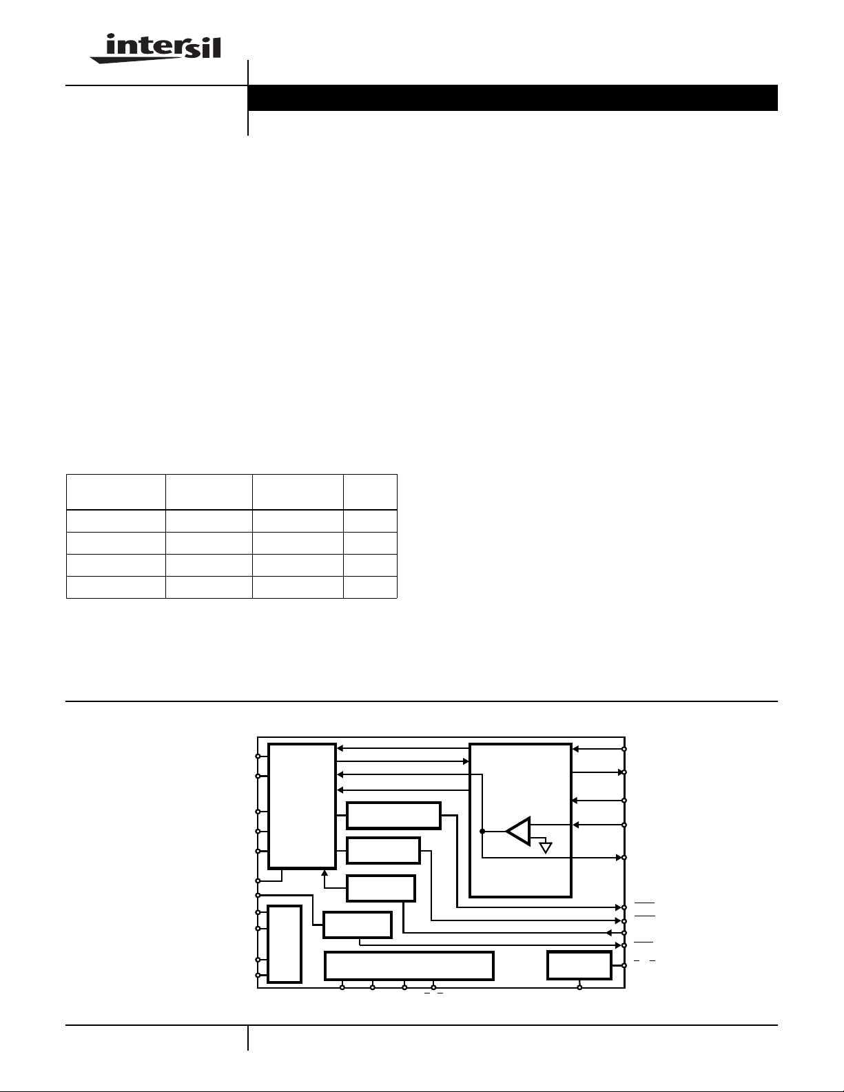
Block Diagram
TIP FEED
TIP SENSE
RING FEED
RING SENSE 1
RING SENSE 2
V
REF
RTI
V
BAT
V
CC
AGND
BGND
62
2-WIRE
INTERFACE
BIAS
V
4-WIRE
INTERFACE
LOOP CURRENT
DETECTOR
FAULT
DETECTOR
CURRENT
LIMIT
RING TRIP
DETECTOR
IIL LOGIC INTERFACE
F1 F0 RS
CAUTION: These devices are sensitive to electrostatic discharge; follow proper IC Handling Procedures.
TST RDI
http://www.intersil.com or 407-727-9207 | Copyright © Intersil Corporation 1999
-
+
RELAY
DRIVER
RX
V
TX
V
RING
- IN 1
OUT 1
SHD
ALM
I
LMT
RTD
RDO
Page 2

HC55171
Absolute Maximum Ratings T
Maximum Supply Voltages
VCC . . . . . . . . . . . . . . . . . . . . . . . . . . . . . . . . . . . . . .-0.5V to +7V
VCC- V
Relay Drivers . . . . . . . . . . . . . . . . . . . . . . . . . . . . . . . .-0.5V to +15V
. . . . . . . . . . . . . . . . . . . . . . . . . . . . . . . . . . . . . . . .90V
BAT
Operating Conditions
Temperature Range
HC55171IM, HC55171IB . . . . . . . . . . . . . . . . . . . . -40oC to 85oC
HC55171CM, HC55171CB . . . . . . . . . . . . . . . . . . . .0oC to 75oC
Relay Drivers . . . . . . . . . . . . . . . . . . . . . . . . . . . . . . . . .+5V to +12V
Positive Power Supply, VCC. . . . . . . . . . . . . . . . . . . . . . . . +5V ±5%
Negative Power Supply, V
CAUTION: Stresses above those listed in “Absolute Maximum Ratings” may cause permanent damage to the device. This is a stress only rating and operationofthe
device at these or any other conditions above those indicated in the operational sections of this specification is not implied
NOTE:
1. θJA is measured with the component mounted on an evaluation PC board in free air.
. . . . . . . . . . . . . . . . . . . .-16V to -80V
BAT
Electrical Specifications Unless Otherwise Specified, Typical Parameters are at T
PARAMETER TEST CONDITIONS MIN TYP MAX UNITS
RINGING TRANSMISSION PARAMETERS
=25oC Thermal Information
A
Thermal Resistance (Typical, Note 1) θJA(oC/W)
PLCC . . . . . . . . . . . . . . . . . . . . . . . . . . . . . . . . . . . . 55
SOIC . . . . . . . . . . . . . . . . . . . . . . . . . . . . . . . . . . . . 70
Maximum Junction Temperature Plastic . . . . . . . . . . . . . . . . .150oC
Maximum Storage Temperature Range. . . . . . . . . . -65oC to 150oC
Maximum Lead Temperature (Soldering 10s) . . . . . . . . . . . . .300oC
(SOIC, PLCC - Lead Tips Only)
Die Characteristics
Transistor Count. . . . . . . . . . . . . . . . . . . . . . . . . . . . . . . . . . . . . .224
Diode Count. . . . . . . . . . . . . . . . . . . . . . . . . . . . . . . . . . . . . . . . . .28
Die Dimensions . . . . . . . . . . . . . . . . . . . . . . . . . . . . . . . . . 175 x 144
Substrate Potential. . . . . . . . . . . . . . . . . . . . . . . . . . . . . . . . . . .V
Process . . . . . . . . . . . . . . . . . . . . . . . . . . . . . . . . . . . . . . .Bipolar-DI
Operating TemperatureRange, V
at 600Ω 2-Wire terminating impedance.
= -24V,VCC= +5V,AGND = BGND = 0V.All AC Parametersare specified
BAT
= 25oC, Min-Max Parameters are over
A
BAT
V
Input Impedance (Note 2) - 5.4 - kΩ
RING
4-Wire to 2-Wire Gain V
AC TRANSMISSION PARAMETERS
RX Input Impedance 300Hz to 3.4kHz (Note 2) - 108 - kΩ
OUT1 Positive Output Voltage Swing RL = 10kΩ (Note 2) +2.5 - - V
OUT1 Negative Output Voltage Swing RL = 10kΩ (Note 2) -4.5 - - V
4-Wire Input Overload Level 300Hz to 3.4kHz RL = 1200Ω, 600Ω Reference
2-Wire Return Loss Matched for 600Ω, f = 300Hz (Note 2) 37 - - dB
2-Wire Longitudinal to Metallic Balance
Off Hook
4-Wire Longitudinal Balance Off Hook 300Hz to 3400Hz (Note 2) - 55 - dB
Longitudinal Current Capability I
Insertion Loss, 2W-4W 0dBmO, 1kHz, Includes Tranhybrid Amp Gain = 3 - ±0.05 ±0.2 dB
Insertion Loss, 4W-2W 0dBmO,1kHz - ±0.05 ±0.2 dB
Insertion Loss, 4W-4W 0dBmO, 1kHz, Includes Tranhybrid Amp Gain = 3 - - ±0.25 dB
to V
RING
(Note 2)
Matched for 600Ω, f = 1000Hz (Note 2) 40 - - dB
Matched for 600Ω, f = 3400Hz (Note 2) 30 - - dB
Per ANSI/IEEE STD 455-1976 300Hz to 3400Hz
(Note 2)
= 40mA, TA = 25oC (Note 2) - 40 - mA
LINE
(Note 2) - 40 - V/V
T-R
- +3.1 - V
58 63 - dB
PEAK
RMS
Frequency Response 300Hz to 3400Hz Referenced to Absolute Level
at 1kHz, 0dBm Referenced 600Ω
63
- ±0.02 ±0.06 dB
Page 3

HC55171
Electrical Specifications Unless Otherwise Specified, Typical Parameters are at T
Operating TemperatureRange, V
at 600Ω 2-Wire terminating impedance. (Continued)
PARAMETER TEST CONDITIONS MIN TYP MAX UNITS
Level Linearity +3 to 0dBm, Referenced to -10dBm (Note 2) - - ±0.10 dB
0 to -40dBm, Referenced to -10dBm (Note 2) - - ±0.12 dB
-40 to -55dBm, Referenced to -10dBm (Note 2) - - ±0.30 dB
Absolute Delay, 2W-4W 300Hz to 3400Hz (Note 2) - - 1.0 µs
Absolute Delay, 4W-2W 300Hz to 3400Hz (Note 2) - - 1.0 µs
Absolute Delay, 4W-4W 300Hz to 3400Hz (Note 2) - 0.95 - µs
Transhybrid Loss VIN = 1V
Total Harmonic Distortion
2-Wire/4-Wire, 4-Wire/2-Wire, 4-Wire/4-Wire
Idle Channel Noise
2-Wire and 4-Wire
PSRR, VCC to 2W 30Hz to 200Hz, RL = 600Ω (Note 2) 30 35 - dB
PSRR, VCC to 4W 45 47 - dB
PSRR, VBAT to 2W 23 28 - dB
Reference Level 0dBm at 600Ω
300Hz to 3400Hz (Note 2)
C-Message (Note 2) - 3 - dBrnC
Psophometric (Note 2) - -87 - dBmp
at 1kH (Note 2) 36 40 - dB
P-P
= -24V,VCC= +5V,AGND = BGND = 0V.All AC Parametersare specified
BAT
= 25oC, Min-Max Parameters are over
A
- - -50 dB
PSRR, VBAT to 4W 33 38 - dB
PSRR, VCC to 2W 200Hz to 3.4kHz, RL = 600Ω (Note 2) 33 35 - dB
PSRR, VCC to 4W 44 46 - dB
PSRR, VBAT to 2W 40 50 - dB
PSRR, VBAT to 4W 50 60 - dB
PSRR, VCC to 2W 3.4kHz to 16kHz, RL = 600Ω (Note 2) 30 34 - dB
PSRR, VCC to 4W 35 40 - dB
PSRR, VBAT to 2W 30 40 - dB
PSRR, VBAT to 4W 40 50 - dB
DC PARAMETERS
Loop Current Programming Range (Note 3) 20 - 60 mA
Loop Current Programming Accuracy -10 - +10 %
Loop Current During Power Denial RL = 200Ω, V
Fault Current, Tip to Ground (Note 2) - 90 - mA
Fault Current, Ring to Ground - 100 - mA
Fault Current, Tip and Ring to Ground (Note 2) - 130 - mA
Switch Hook Detection Threshold 9 12 15 mA
= -48V - ±4-mA
BAT
Ring Trip Comparator Voltage Threshold -0.28 -0.24 -0.22 V
Thermal ALARM Output Safe Operating Die Temperature Exceeded
(Note 2)
Dial Pulse Distortion (Note 2) - 0.1 0.5 ms
- 160 -
o
64
C
Page 4

HC55171
Electrical Specifications Unless Otherwise Specified, Typical Parameters are at T
Operating TemperatureRange, V
= -24V,VCC= +5V,AGND = BGND = 0V.All AC Parametersare specified
BAT
= 25oC, Min-Max Parameters are over
A
at 600Ω 2-Wire terminating impedance. (Continued)
PARAMETER TEST CONDITIONS MIN TYP MAX UNITS
UNCOMMITTED RELAY DRIVER
On Voltage, V
OL
IOL (RDO) = 30mA - 0.2 0.5 V
Off Leakage Current - ±10 ±100 µA
TTL/CMOS LOGIC INPUTS (F0, F1, RS, TST, RDI)
Logic Low Input Voltage 0 - 0.8 V
Logic High Input Voltage 2.0 - 5.5 V
Input Current IIH, 0V ≤ VIN≤ 5V - - -1 µA
Input Current IIL, 0V ≤ VIN≤ 5V - - -100 µA
LOGIC OUTPUTS (SHD, RTD, ALM)
Logic Low Output Voltage I
Logic High Output Voltage I
= 800µA - 0.1 0.5 V
LOAD
= 40µA 2.7 - 5.5 V
LOAD
POWER DISSIPATION --Power Dissipation On Hook VCC = +5V, V
VCC = +5V, V
Power Dissipation Off Hook VCC = +5V, V
= -80V, R
BAT
= -48V, R
BAT
= -24V, R
BAT
= ∞ - 300 - mW
LOOP
= ∞ - 150 - mW
LOOP
LOOP
= 600Ω,
- 280 - mW
IL = 25mA
I
CC
I
BAT
VCC = +5V, V
VCC = +5V, V
VCC = +5V, V
= -80V, R
BAT
= -48V, R
BAT
= -24V, R
BAT
VCC = +5V, VB- = -80V, R
VCC = +5V, VB- = -48V, R
VCC = +5V, VB- = -24V, R
= ∞ -36mA
LOOP
= ∞ -25mA
LOOP
= ∞ - 1.9 5 mA
LOOP
= ∞ - 3.6 7 mA
LOOP
= ∞ - 2.6 6 mA
LOOP
= ∞ - 2.3 4.5 mA
LOOP
NOTES:
2. These parameters arecontrolledby design or processparameters and are notdirectlytested. These parameters arecharacterized upon
initial design release, upon design changes which would affect these characteristics, and at intervals to assure product quality and
specification compliance.
3. This parameter directly affects device junction temperature. Refer to Power Dissipation discussion of data sheet for design information.
65
Page 5
Functional Diagram
HC55171
TF
TIP
SENSE
RING
SENSE 1
RING
SENSE 2
RF
R
2R
-
+
2R
25K
-
+
25K
R
R
R/2
R/20
TA
RA
90K
TF
25
14
15
16
26
-
+
4.5K
100K
100K
100K
100K
4.5K
R
R
R
R
90K
90K
RF
-
+
V
RX
17 12
+2V
OUT 1
VB/2
REF
SHD
RTD
-
+
-IN 1
OP AMP
V
RING
13 24 19 2
FAULT
DET
GM
V
-
+
TX
THERM
LTD
RF2
V
CC
BIAS
NETWORK
SH
TSD
GK
RFC
AGND
IIL LOGIC INTERFACE
1
22
BGND
27
V
BAT
4
F1
5
F0
6
RS
9
TST
7
SHD
8
RTD
10
ALM
21
RDO
R = 108kΩ
3
V
REF
18
HC55171 DEVICE TRUTH TABLE
F1 F0 STATE
0 0 Loop power Denial Active
0 1 Power Down Latch RESET, Power on
RESET
10
RD Active
1 1 Normal Loop feed
The truth table for the internal logic of the HC55171 is provided in the above table. This family of ringing SLICS can be
configured to support traditional unbalanced ringing and thru
SLIC balanced ringing. Refer to the HC5509A1R3060 for
unbalanced ringing application information. The device operating states used by thru SLIC ringing applications are loop
power denial and normal feed. During loop power denial, the
tip and ring amplifiers are disabled (high impedance) and the
DC voltage of each amplifier approaches ground. The SLIC
will not provide current to the subscriber loop during this mode
and will not detect loop closure. Voice transmission occurs
during the normal loop feed mode. During normal loop feed
the SLIC is completely operational and performs all transmission and supervisory functions.
28
RTINU I
11
LMT
20
RDI
Power Dissipation
Careful thermal design is required to guarantee that the
maximum junction temperature of 150
o
C of the device is not
exceeded. The junction temperature of the SLIC can be calculated using:
TJTAθJAICCVCCI
BATVBATILOOP
()2R
•()–+()+=
LOOP
Where TAis maximum ambient temperature and θJAis junction to air thermal resistance (and is package dependent).
The entire term in parentheses yields the SLIC power dissipation. The power dissipation of the subscriber loop does
not contribute to device junction temperature and is subtracted from the power dissipation term. Operating at 85
the maximum PLCC SLIC power dissipation is 1.18W. Likewise, the maximum SOIC SLIC power dissipation is 0.92W.
(EQ. 1)
o
C,
66
Page 6
HC55171
Circuit Operation and Design Information
Introduction
The HC55171 is a high voltage Subscriber Line Interface Circuit (SLIC) specifically designed for through SLIC ringing
applications. Through SLIC ringing applications are broadly
defined as any application that requires ringing capability but
does not have the standard wired central office interface. The
most common implementation of the ringing SLIC is in the
analog pots port. The analog pots port provides the ringing
function as well as interface compatibility with answering and
fax machines.
Subscriber Line Interface Basics
The basic SLIC provides DC loop current to power the handset,
supports full duplex analog transmission between the handset
and CODEC, matches the impedance of the SLIC to the
impedance of the handset and performs loop supervision functions to detect when the handset is off hook.
adds through the SLIC ringing capability to this suite of features.
The analog interfaces of the SLIC are categorized as the
2-wire interface(high voltageDC,differential AC) and the 4-wire
interface (low voltage DC, single ended AC).
DC Loop Current
The Tip and Ring terminals of the subscriber line circuit are
biased at negative potentials with respect to ground. The Tip
terminal DC potential is slightly negative with respect to
ground, and the ring terminal DC potential is slightly positive
with respect to the battery voltage (resulting in a large negative voltage). The HC55171 typical Tip DC voltage is -4V and
the typical ring DC voltage is defined as V
ple, when the battery voltage is -24V the ring voltage is -20V.
To clearly comprehend the Tip and Ring interface it is helpful
to understand that the handset and the SLIC constitute a DC
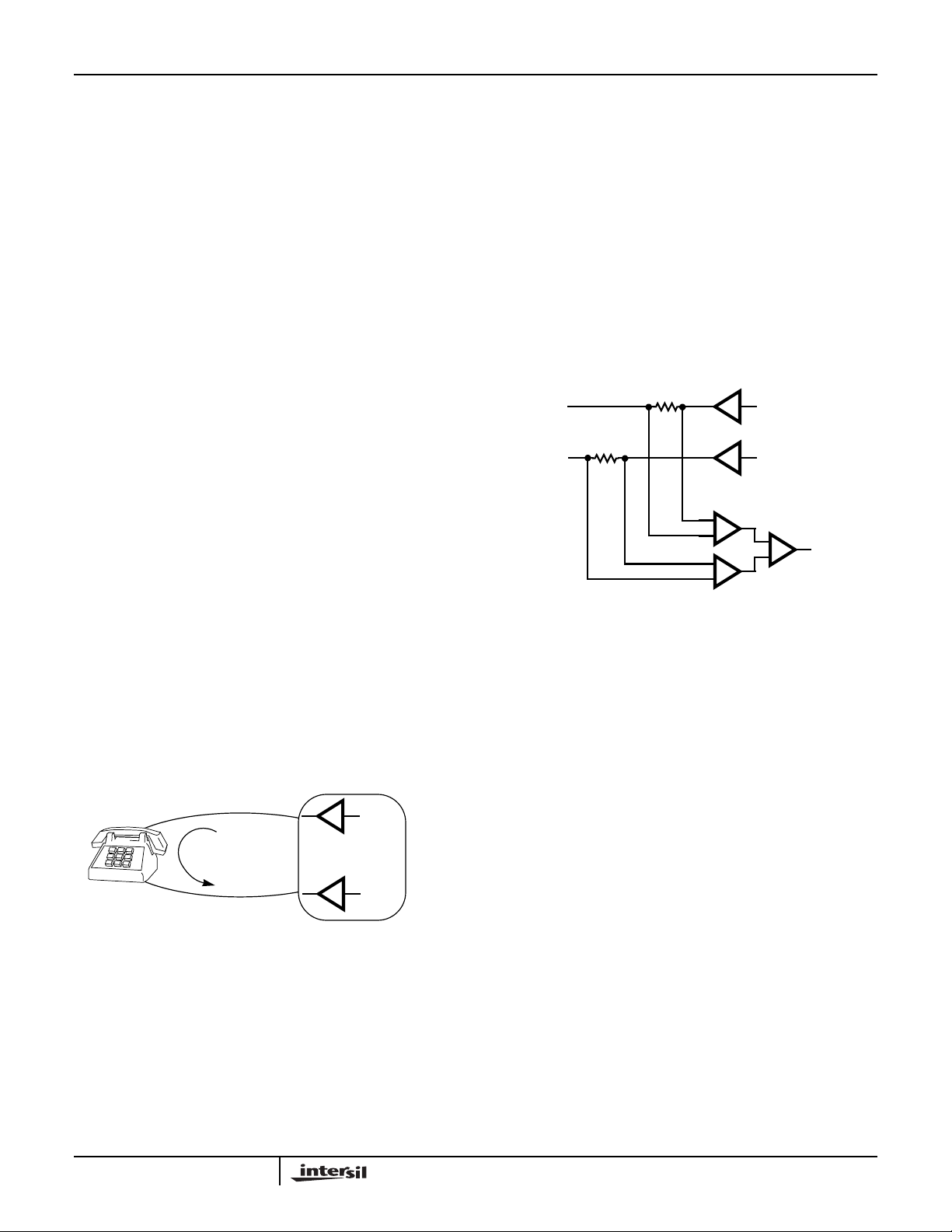
and AC current loop as shown in Figure 1. The loop is often
referred to as the subscriber loop.
LOOP
CURRENT
FIGURE 1. SUBSCRIBER LOOP
When the handset is on hook (idle) the phone is an open circuit load and the DC loop current is zero. The SLIC can still
provide AC transmission in this condition, which supports
caller id services. The DC resistance of the off hook handset
is typically 400Ω. Since the Tip DC voltage is more positive
than the ring DC voltage, DC loop current flows from Tip to
Ring when the handset is off hook. The SLIC is designed
with feedback to limit the maximum loop current when the
handset is off hook.
The ringing SLIC
+ 4V. For exam-
BAT
TIP
RING
SLIC
Full Duplex Analog Transmission
Familiarity with the signal paths of the SLIC is critical in
understanding the full duplex transmission capability of the
device. The analog interfaces of the SLIC are categorized as
2-wire interfaces and 4-wire interfaces.
The 2-wire interface of the SLIC consists of the bidirectional
Tip and Ring terminals of the device. A differential transmitter drives AC signals out of the Tip and Ring terminals to the
handset. A differential receiver across Tip and Ring receives
AC signals from the handset. The differential receiver is connected across sense resistors that are in the Tip and Ring
signal paths. The differential transmitter and receiver concept is depicted in Figure 2.
DIFFERENTIAL
TRANSMITTER
-1
-
+
-
+
FIGURE 2. DIFFERENTIAL TRANSMIT/RECEIVE CONCEPT
-
+
DIFFERENTIAL
RECEIVER
Since the receiver is connected across the transmit signal
path, one may deduce that in addition to receiving signals
from the handset, the receiver will detect part of the transmit
signal. Indeed this does occur and is the reason that all SLIC
circuits require a hybrid balance or echo cancellation function.
The 4-wire interface of the SLIC consists of the receive
(VRX) and transmit (OUT1) terminals. The 4-wire interfaces
are single ended signal paths. The receiver is a dedicated
input port and the transmitter is a dedicated output port. The
4-wire receive input of the SLIC drives the 2-wire differential
transmitter and the 2-wire differential receiver drives the 4wire transmit output.
The complete signal path for voice signals includes two digital data busses, a CODEC and a SLIC. There is a receive
data bus and transmit data bus, each with an independent 3wire serial interface. The CODEC contains a coder and
decoder. The coder converts the SLIC analog transmit output to digital data for the transmit data bus. The receive digital data bus is converted to analog data and drives the SLIC
receive input.
The CODECs use logarithmic compression schemes to
extend the resolution of the 8-bit data to 14 bits. The
accepted compression schemesareA-law(Intersil CODEC CD22357A) and µ-law (Intersil CODEC - CD22354A). The
complete signal path from the handset to the CODEC is
shown in Figure 3.
67
Page 7

HC55171
SLIC
TIP
V
RX
OUT1
RING
FIGURE 3. COMPLETE VOICE SIGNAL PATH FIGURE 4. SLIC IMPEDANCE DIAGRAM
CODEC
RX
OUT
TX
ANALOG DIGITAL
PCM
IN
IN
PCM
OUT
Impedance Matching
Impedance matching is used to match the AC source impedance of the SLIC to the AC source impedance of the load.
When the impedance is matched, the voltage level at the
receive input of the SLIC will be the same voltage levelthatis at
the 2-wire differential output (i.e., Tip and Ring). Impedance
matching applies only to the 2-wire interface, not the 4-wire
interface.
Slic AC signal power levels are most commonly assigned the
units dBmO. The term dBmO refers to milliwatts in a 600Ω
load. The typical AC power level is 0dBmO which is 1mW
referenced to a 600Ω load. The relationship between dBmO
and V
dBmO 10 1000
is provided in Equation 2.
RMS
V
()
------------------------
log⋅=
⋅
RMS
600
2
(EQ. 2)
Substituting 0dBmO into the equation should result in
0.7746 V
. For sinusoidal signals, multiply the RMS
RMS
voltage by 1.414 to obtain the peak sinusoidal voltage.
The SLIC impedance matching is achieved by applying a feed
back loop from the transmit output of the SLIC to the receive
input of the SLIC. The transmit output voltage of the HC55171
is proportional to the loop current (DC + AC) flowing in the subscriber loop. The impedance matching feedback only uses the
AC portion of the transmit output voltage. Applying a voltage
gain to the feedback term and injecting it into the receive signal
path, will cause the SLIC to “synthesize” a source impedance
that is nonzero. Recall that the impedance matching sets the
SLIC source impedance equal to the load impedance.
The SLIC application circuit requires external sense resistors
in the Tip and Ring signal paths to achieve the differential
receive function. The sense resistors contribute to the source
impedance of the SLIC and are accounted for in the design
equations. Specifically, if the load impedance is 600Ω and
each sense resistor is 50Ω, the SLIC must synthesize an
additional source impedance of 500Ω (i.e., 600Ω - 2(50Ω)).
In addition to the sense resistors, some applications may use a
protection resistor in each of the Tip and Ring leads as part of a
surge protection network. These resistors also contribute to the
SLIC source impedance and can be easily accounted for in the
design equations. If 50Ω protection resistors are added to the
prior example, the SLIC would then have to synthesize 400Ω to
match the load (i.e., 600Ω - 2(50Ω) - 2(50Ω)). A diagram
LOAD IMPEDANCE
RSYNTH
RSRP
RSRP
RSYNTH
SLIC SOURCE IMPEDANCE
TIP
RING
-1
showing the impedance terms is shown in Figure 4.
Loop Supervision
The SLIC must detect when the subscriber picks up the
handset when the SLIC is not ringing the phone and when
the SLIC is ringing the phone. The HC55171 uses a switch
hook detector output to indicate loop closure when the SLIC
is not ringing the phone. When the SLIC is ringing the
phone, loop closure is indicated by the ring trip detector.
(Recall from earlier discussions that the subscriber loop is
open when the handset is on hook and closed when off
hook. The DC impedance of the handset when off hook is
typically 400Ω.)
When the handset is off hook, DC loop current flows from
Tip to Ring and the transmit output voltage increases to a
negative value. In addition to interfacing to the CODEC and
providing the feedback for impedance matching, the transmit
output also drives the input to a voltage comparator. When
the comparator threshold is exceeded, the
SHD output goes
to a logic low, indicating the handset is off hook. When the
call is terminated and the handset is returned on hook, the
transmit voltage decreases to zero, crossing the comparator
threshold and setting
SHD to a logic high.
Loop closure must also be detected when the SLIC is ringing
the handset. The balanced ringing output of the SLIC coincides with a zero DC potential between Tip and Ring. Therefore the ring trip must be designed around an AC only
waveform at the transmit output. When the SLIC is ringing
and the handset is on hook, the echo of the ringing signal is
at the transmit output. When the handset goes off hook, the
amplitude of the ringing echo increases. The increase in
amplitude is detected by an envelope detector. When the
echo increases, the envelope detector output increases and
exceeds the ring trip comparator threshold. Then
RTD goes
to a logic low, indicating the handset is off hook. When the
system controller detects a logic low on
RTD, the ringing is
turned off and the Tip and Ring terminals return to their
typical negative DC potentials.
Design Equations and Operational Theory
The following discussion separates the SLICS’s operation
into its DC and AC path, then follows up with additional circuit design and application information.
68
Page 8

HC55171
DC Operation of Tip and Ring Amplifiers
SLIC in the Active Mode
The tip and ring amplifiers are voltage feedback op amps
that are connected to generate a differential output (e.g., if
tip sources 20mA then ring sinks 20mA). Figure 5 shows the
connection of the tip and ring amplifiers. The tip DC voltage
is set by an internal +2V reference, resulting in -4V at the
output. The ring DC voltage is set by the tip DC output voltage and an internal V
at the output. (See Equation 3, Equation 4 and Equation 5.)
V
TIPFEEDVC
R
P1
==
R
S1
V
RINGFEEDVD
V
RINGFEEDVDVBAT
TIP
/2 reference, resulting in V
BAT
R
-----------
2V–
R2⁄
V
BAT
-------------- -
2
4V–== =
R
–
1
--- -+
V
R
TIPFEED
4+==
R
TIP FEED
-
+
-
V
C
+
TRANSVERSAL
AMP
90kΩ 90kΩ
R/20
R/2
TA
-
+
+4V
BAT
(EQ. 3)
R
--- -
R
(EQ. 4)
(EQ. 5)
V
RX
R
R
OUT1
V
RING
INTERNAL
+
-
+2V REF
V
TX
R
IL1
R
IL2
RF2
GM
-
+
Current Limit
The tip feed to ring feed voltage (Equation 3 minus
Equation 5) is equal to the battery voltage minus 8V. Thus,
with a 48 (24) volt battery and a 600Ω loop resistance,
including the feed resistors, the loop current would be
66.6mA (26.6mA). On short loops the line resistance often
approaches zero and there is a need to control the maximum
DC loop current.
Current limiting is achieved by a feedback network (Figure 5)
that modifies the ring feed voltage (V
) as a function of the
D
loop current. The output of the Transversal Amplifier (TA) has
a DC voltage that is directly proportional to the loop current.
This voltage is scaled by R
IL1
and R
. The scaled voltage
IL2
is the input to a transconductance amplifier (GM) that compares it to an internal reference level. When the scaled voltage exceeds the internal reference level, the
transconductance amplifier sources current. This current
charges C
voltage (V
effectively reduces the tip feed to ring feed voltage (V
in the positive direction causing the ring feed
IL
) to approach the tip feed voltage (VC). This
D
T-R
and holds the maximum loop current constant.
The maximum loop current is programed by resistors R
and R
as shown in Equation 7 (Note: R
IL2
is typically
IL1
IL1
100kΩ).
I
LIMIT
-10
0.6()R
------------------------------------------------- -=
0
V
-5
+()
IL1RIL2
()
200xR
IL2
TIP FEED
= -4V
(EQ. 7)
CONSTANT VOLTAGE
REGION
).
R
OUT1
, V
P2
RX
RING
V
GROUNDED FOR
DC ANALYSIS
R
S2
RING FEED
-
+
+
V
D
-
90kΩ
V
-
C
IL
BAT
+
2
FIGURE 5. OPERATION OF THE TIP AND RING AMPLIFIERS
Transmit Output Voltage
The transmit output voltage in terms of loop current is
expressed as 200x I
. The 200 term is actually formed
LOOP
by the sum of twice the sense resistors and is shown in the
following equation.
200 I
× 2RS1⋅ 2RS2⋅+()I
LOOP
×=
LOOP
(EQ. 6)
This is a relationship that is critical when modifying the
sense resistor (R
S1,RS2
). The 200 term factors into the loop
current limit and loop detector functions of the SLIC.
69
-15
V
RING FEED
-20
TIP AND RING VOLTAGE (V)
-25
CURRENT LIMIT
REGION I
0
FIGURE 6. V
= 25mA
LOOP
250
LOOP RESISTANCE (Ω)
vs RL(V
T-R
500 750
= -24V, I
BAT
LIMIT
Figure 6 illustrates the relationship between V
= 25mA)
T-R
= -20V
∞
and the
loop resistance. The conditions are shown for a battery
voltage of -24V and the loop current limit set to 25mA. For an
open circuit loop the tip feed and ring feed are at -4V and
-20V respectively. When the loop resistance decreases from
infinity to about 640Ω the loop current (obeying Ohm’s Law)
increases from 0mA to the set loop current limit. As the loop
resistance continues to decrease, the ring feed voltage
approaches the tip feed voltage as a function of the
programmed loop current limit (Equation 7).
Page 9

HC55171
AC Voltage Gain Design Equations
The HC55171 uses feedback to synthesize the impedance
at the 2-wire tip and ring terminals. This feedback network
defines the AC voltage gains for the SLIC.
The 4-wire to 2-wire voltage gain (V
feedback loop shown in Figure 7. The feedback loop senses
the loop current through resistors R
age drop and multiplies it by 2 to produce an output voltage at
the V
pin equal to +4RS∆IL. The VTXvoltage is then fed into
TX
the -IN1 input of the SLIC’s internal op amp. This signal is multiplied by the ratio R
Z0/RRF
and fed into the tip current summing
node via the OUT1 pin. (Note: the internal V
(ring feed amplifier) and the internal +2V reference (tip feed
amplifier) are grounded for the AC analysis .)
The current into the summing node of TF amp is equal to:
I
OUT1
=
4RSIL∆
--------------------
–
R
R
Z0
-----------
R
RF
Equation 9 is the node equation for the tip amplifier summing
node. The current in the tip feedback resistor (I
Equation 7.
4RSIL∆
--------------------
I
–
–
R
–
I
R
R
4RSIL∆
--------------------
R
R
Z0
-----------
R
RF
R
Z0
-----------
R
RF
V
RX
-----------+ 0=
R
V
RX
-----------+=
R
to VTR) is set by the
RX
and RS2, sums their volt-
S1
/2 reference
BAT
) is given in
R
(EQ. 8)
(EQ. 9)
(EQ. 10)
R
∆
SIL
Z0
-----------
R
RF
VRX+
(EQ. 15)
24– R
×
I
∆
L
------------------------------------------------------------------------------=
++++
R
LRP1RP2RS1RS2
Equation 15 simplifies to
2V
400 IL∆–
RX
I
∆
----------------------------------------=
L
Solving for ∆I
V
RX
∆
-----------=
I
L
600
800
results in
L
(EQ. 16)
(EQ. 17)
Equation 17 is the loop current with respect to the feedback
network. From this, the 4-wire to 2-wire and the 2-wire to
4-wire AC voltage gains are calculated. Equation 18 shows
the 4-wire to 2-wire AC voltage gain is equal to 1.00.
V
RX
-----------
A
4W 2W–
V
TR
-----------
V
RX
()
I∆
LRL
-------------------- -
V
RX
600()
600
--------------------------- 1== = =
V
RX
(EQ. 18)
Equation 19 shows the 2-wire to 4-wire AC voltage gain is
equal to -0.333.
R
A
2W 4W–
V
OUT1
-------------------
V
TR
Z0
∆
SIL
I∆
()
LRL
-----------
R
RF
4– R
----------------------------------------- -
V
RX
-----------
200–
600
----------------------------------
V
RX
-----------
600()
600
1()
1
-- -–== = =
3
(EQ. 19)
The AC voltage at V
V
()R()=
CIR
4– RSIL∆
V
C
and the AC voltage at V
VD4RSIL∆
The values for R
is then equal to:
C
R
Z0
-----------
V
+=
R
R
Z0
-----------
R
RF
RX
RF
is:
D
–=
V
RX
and RRFare selected to match the
Z0
(EQ. 11)
(EQ. 12)
(EQ. 13)
impedance requirements on tip and ring, for more
information refer to AN9607 “Impedance Matching Design
Equations for the HC5509 Series of SLICs”. The following
loop current calculations will assume the proper R
R
values for matching a 600Ω load.
RF
∆I
The loop current (
) with respect to the feedback network, is
L
calculated in Equations 14 through 17. Where R
R
= 40kΩ, RL = 600Ω, RP1 = RP2 = RS1 = RS1 = 50Ω.
RF
V
–
∆
------------------------------------------------------------------------------=
I
L
++++
R
LRP1RP2RS1RS2
Substituting the expressions for V
CVD
and V
C
D
Z0
and
Z0
= 40kΩ,
(EQ. 14)
Impedance Matching
The feedback network, described above, is capable of
synthesizing both resistive and complex loads. Matching the
SLIC’s 2-wire impedance to the load is important to maximize power transfer and maximize the 2-wire return loss.
The 2-wire return loss is a measure of the similarity of the
impedance of a transmission line (tip and ring) and the
impedance at it’s termination. It is a ratio, expressed in decibels, of the power of the outgoing signal to the power of the
signal reflected back from an impedance discontinuity.
Requirements for Impedance Matching
Impedance matching of the HC55171 application circuit to the
transmission line requires that the impedance be matched to
points “A” and “B” in Figure 7. To do this, the sense and protection resistors R
P1,RP2,RS1
for by the feedback network to make it appear as if the output
of the tip and ring amplifiers are at points “A” and “B”. The
feedback network takes a voltage that is equal to the voltage
drop across the sense resistors and feeds it into the summing
node of the tip amplifier. The effect of this is to cause the tip
feed voltage to become more negative by a value that is proportional to the voltage drop across the sense resistors R
and RS1. At the same time the ring amplifier becomes more
positive by the same amount to account for resistors R
and RS2.
The net effect cancels out the voltage drop across the feed
resistors. By nullifying the effects of the feed resistors the
and RS2must be accounted
P1
P2
70
Page 10

∆
I
HC55171
feedback circuitry becomes relatively easy to match the
impedance at points “A” and “B”.
Impedance Matching Design Equations
Matching the impedance of the SLIC to the load is
accomplished by writing a loop equation starting at V
going around the loop to V
.
C
and
D
The loop equation to match the impedance of any load is as
follows (note: V
R
4RSIL∆–
∆ 8RSIL∆–
-----------
R
RF
V
IN
VIN∆ IL∆ 8RS–
= 0 for this analysis):
RX
Z0
2R
+++
∆–∆ RLIL∆ 2RSIL∆ 4RSIL∆–
SILVIN
R
Z0
-----------
4R
∆ RLIL∆++=
Z0
SIL
++=
4R
SRL
R
RF
R
-----------
R
RF
R
Z0
-----------
R
RF
(EQ. 20)
(EQ. 21)
(EQ. 22)
Equation 22 can be separated into two terms, the feedback
(-8R
S(RZ0/RRF
V
∆
IN
------------- 8– R
∆
I
L
)) and the loop impedance (+4RS+RL).
R
Z0
-----------
S
R
RF
4R
+[]+=
SRL
(EQ. 23)
R
L
∆V
LOAD
+
IN
-
SLIC
8RS
R
Z0
------------ -
4RS+
R
RF
FIGURE 8. SCHEMATIC REPRESENTATION OF EQUATION 20
The result is shown in Equation 23. Figure 8 is a schematic
representation of Equation 18. To match the impedance of
the SLIC to the impedance of the load, set:
R
Z0
-----------
8R
S
R
RF
If R
is made to equal 8RS then:
RF
4R
=+
SRL
RZ04RSRL=+
Therefore to match the HC5517, with R
equal to 50Ω,toa
S
(EQ. 24)
(EQ. 25)
600Ω load:
R
8RS850Ω()400Ω== =
RF
(EQ. 26)
and
R
Z0RL
To prevent loading of the V
R
RF
KR
Z0
4– RS600Ω 200Ω– 400Ω== =
output, the value of RZ0and
TX
are typically scaled by a factor of 100:
40kΩ= KR
RF
40kΩ=
(EQ. 27)
(EQ. 28)
4– RSIL∆()
----------------------------- -
I
R
TIP
A
R
+
R
∆I
L
P1
R
Z0
------------ -
R
RF
∆I
+
-
R
S1
V
RX
------------ -+=
R
L
-
I
R
R
-
+
-
V
C
+
R
R
R/20
R/2
V
4– R
=
C
S
Since the impedance matching is a function of the voltage
gain, scaling of the resistors to achieve a standard value is
recommended.
For complex impedances the above analysis is the same.
KRRF40kΩ=()KRZ0100 Resistive 200–()
Reactive
--------------------------+=
100
(EQ. 29)
Refer to application note AN9607 (“Impedance Matching
Design Equations for the HC5509 Series of SLICs”) for the
values of KRRFand KRZ0for many worldwide typical line
impedances.
V
TR
R
∆V
-
∆I
L
IN
L
+
RP1 = RP2 = RS1 = RS2 = R
S
-
+
∆I
L
+
B
RING
R
∆I
R
P2
S2
∆I
L
-
L
+-
+
90kΩ 90kΩ
-
+
+
V
D
-
VD4RS=
Through SLIC Ringing
The HC55171 uses linear amplification to produce the ringing
signal. As a result the ringing SLIC can produce sinusoid,
trapezoid or square wave ringing signals. Regardless of the
wave shape, the ringing signal is balanced. The balanced
waveform is another way of saying that the tip and ring DC
potentials are the same during ringing. The following figure
shows the Tip and Ring waveforms for sinusoid and trapezoid
wave shapes as can be displayed using an oscilloscope.
Pertinent Bellcore Ringing Specifications
Bellcore has defined bounds around the existing unbalanced
FIGURE 7. AC VOLTAGE GA
ringing signal that is supplied by the central office. The
71
Page 11

HC55171
GROUND
TIP
RING
BATTERY
(A) SINUSOID
GROUND
TIP
RING
BATTERY
(B) TRAPEZOID
FIGURE 9. BALANCED RINGING WAVESHAPES
HC55171 ringing SLIC meets the REN drive requirement, the
crest factor limitations and the minimum RMS ringing voltage.
The foremost requirement is that the ringing source must be
able to drive 5 REN. A REN is a ringer equivalence number
modeled by a 6.93kΩ resistor in series with a 8µF capacitor
(see Figure 10). The impedance of 1 REN at 20Hz is approximately 7kΩ. 5 REN is equivalent to five of the networks in
parallel. Figure 10 provides the Bellcore REN models.
The crest factor of the ringing waveform is the ratio of the
peak voltage to the RMS voltage. For reference, the crest
factor of a sinusoid is 1.414 and of a square wave is 1.0.
Bellcore defines the crest factor range from 1.2 to 1.6. A signal with a crest factor between 1.2 and 1.414 resembles the
trapezoid of Figure 9. A signal with a crest factor between
1.414 and 1.6 resembles a “rounded triangular” wave shape
and is an inefficient waveform for the ringing SLIC.
40µF
8µF
FIGURE 10. BELLCORE RINGER EQUIVALENCE MODELS
1386Ω
5 REN
6930Ω
1 REN
The third pertinent Bellcore requirement is the that RMS ringing
voltage must be greater than 40V
ment. The HC5517 is able to deliver 40V
at the telephone instru-
RMS
at the end of
RMS
500Ω loops. The 500Ω loop drive capability of the HC5517 is
achieved with trapez oidal ringing.
Sinusoidal Ringing
The HC55171 uses the same sinusoidal application circuit
as the HC5517. The only difference being the values of three
components in the ring trip filter. The following table lists the
components and the different values required by each
device. All reference designators refer to the application
circuit published in the HC5517 and HC55171 data sheet.
TABLE 1. RING TRIP COMPONENT DIFFERENCES
COMPONENT HC5517 COMPONENT HC55171
R
15
R
17
C
10
47kΩ R
56.2kΩ R
1.0µFCRT0.47µF
RT3
RT1
51.1kΩ
49.9kΩ
The sinusoidal circuit published in the HC5517 can be used
as an additional reference circuit for the HC55171. To generate a sinusoid ringing signal, two conditions must be met on
the ringing (V
) input of the SLIC.
RING
The first condition is that a positive DC voltage, which is directly
related to the battery voltage, must be present at the ringing
input. The DC voltage is used to force the Tip and Ring DC outputs to half the battery voltage. Having both the Tip and Ring
amplifiers biased at the same DC voltage during ringing is one
characteristic of balanced ringing. The centering voltage (V
C
can be calculated from the following equation.
V
V
BAT
-------------- -
C
2
20⁄=
4–
(EQ. 30)
Substituting values of battery voltage, the centering voltage
is +1.8V for a -80V battery and +1.3V for a -60V battery.
The second condition that must be met for sinusoidal ringing
is a low level ringing signal must be applied to the ringing
input of the SLIC. The AC signal that is present at V
RING
will
be amplified by a gain of 20 through the Tip amplifier and a
then inverted through the ring amplifier, resulting in a differential gain of 40. The maximum low level amplitude that can
be injected for a given battery voltage can be determined
from the following equation.
V
RING Max()VBAT
8–()20⁄=
(EQ. 31)
The maximum output swing may be increased by driving the
V
negative by 200mV. Equation 31 can then by
RING
rewritten as:
V
RING Max()VBAT
5–()20⁄=
(EQ. 32)
Exceeding the maximum signal calculated from the above
equation will cause the peaks of the sinusoid to clip at
ground and battery. The compression will reduce the crest
factor of the waveform, producing a trapezoidal waveform.
This is just one method, though inefficient, for achieving trapezoidal ringing. The application circuit provided with the
HC55171 has been specifically developed for trapezoidal
ringing and may also be used with the HC5517.
Trapezoidal Ringing
The trapezoidal ringing waveform provides a larger RMS
voltage to the handset. Larger RMS voltages to the handset
provide more power for ringing and also increase the loop
length supported by the ringing SLIC.
The HC55171 trapezoidal ringing application circuit will operate for loop lengths ranging from 0Ω to 500Ω. In addition, one
)
72
Page 12

HC55171
set of component values will satisfy the entire ringing loop
range of the SLIC. A single resistor sets the open circuit RMS
ringing voltage, which will set the crest factor of the ringing
waveform. The crest factor of the HC55171 ringing waveform
is independent of the ringing load (REN) and the loop length.
Another robust feature of the HC55171 ringing SLIC is the
ring trip detector circuit. The suggested values for the ring trip
detector circuit cover quite a large range of applications.
The assumptions used to design the trapezoidal ringing
application circuit are listed below:
• Loop current limit set to 25mA.
• Impedance matching is set to 600Ω resistive.
• 2-wire surge protection is not required.
• System able to monitor
RTD and SHD.
• Logic ringing signal is used to drive RC trapezoid network.
Crest Factor Programming
As previously mentioned, a single resistor is required to set
the crest factor of the trapezoidal waveform. The only design
variable in determining the crest factor is the battery voltage.
The battery voltage limits the peak signal swing and
therefore directly determines the crest factor.
A set of tables will be provided to allow selection of the crest
factor setting resistor. The tables will include crest factors
below the Bellcore minimum of 1.2 since many ringing SLIC
applications are not constrained by Bellcore requirements.
TABLE 2. CREST FACTOR PROGRAMMING RESISTOR FOR
V
= -80V
BAT
R
TRAP
0Ω 1.10 65.0 825Ω 1.25 57.6
389Ω 1.15 62.6 964Ω 1.30 55.4
640Ω 1.20 60.0 1095Ω 1.35 53.3
CF RMS R
TRAP
CF RMS
The RMS voltage listed in the table is the open circuit RMS
voltage generated by the SLIC.
TABLE 3. CREST FACTOR PROGRAMMING RESISTOR FOR
R
TRAP
0Ω 1.10 60.9 1010Ω 1.25 53.7
500Ω 1.15 58.3 1190Ω 1.30 51.6
791Ω 1.20 55.9 1334Ω 1.35 49.7
TABLE 4. CREST FACTOR PROGRAMMING RESISTOR FOR
R
TRAP
0Ω 1.10 52.5 1330Ω 1.25 45.9
660Ω 1.15 49.8 1600Ω 1.30 44.1
1040Ω 1.20 47.8 1800Ω 1.35 42.5
= -75V
V
BAT
CF RMS R
= -65V
V
BAT
CF RMS R
TRAP
TRAP
CF RMS
CF RMS
TABLE 5. CREST FACTOR PROGRAMMING RESISTOR FOR
V
= -60V
BAT
R
TRAP
0Ω 1.10 48.2 1460Ω 1.25 42.0
740Ω 1.15 45.6 1760Ω 1.30 40.4
1129Ω 1.20 43.7 2030Ω 1.35 38.8
CF RMS R
TRAP
CF RMS
Ringing Voltage Limiting Factors
As the load impedance decreases (increasing REN), the
feedback used for impedance synthesis slightly attenuates
the ringing signal. Another factor that attenuates the ringing
signal is the voltage divider formed by the sense resistors
and the impedance of the ringing load. As the load impedance decreases, the 100Ω of sense resistors becomes a
larger percentage of the load impedance.
If surge protection resistance must be used with the
trapezoidal circuit, the loop length performance of the circuit
will decrease. The decrease in ringing loop length is caused
by the addition of protection resistors in series with the Tip
and Ring outputs. The amount of protection resistance that
is added will subtract directly from the loop length. For example if 30Ω protection resistors is used in each of the Tip and
Ring leads, the ringing loop length will decrease by a total of
60Ω. Therefore, subtracting 60Ω from the graphs will provide
the reduced loop length data.
Lab Measurements
The lab measurements of the trapezoidal ringing circuit were
made with the crest factor programming resistor set to 0Ω
and the battery voltage set to -80V. The Bellcore suggested
REN model was used to simulate the various ringing loads.
A resistor in series with the Tip terminal was used to emulate
loop length.
A logic gate is used to drive the RC shaping network. When
the crest factor programming resistor is set to 0Ω, the output
impedance of the logic gate results in a 0.8V/ms slewing
voltage on C
TRAP
.
Each graph shows the RMS ringing voltage into a fixed REN
load versus loop length. The ringing voltage was measured
across the test load. Each test also verified proper operation
of the ring trip detector. Proper ring trip detector operation is
defined as a constant logic high while ringing and on hook
and a constant logic low when off hook is detected. The
component values in the application circuit provide a ring trip
response in the 100ms to 150ms range.
73
Page 13

HC55171
60
59
58
57
RMS RINGING VOLTAGE
56
0 100 200 300 400 500
LOOP IMPEDANCE
FIGURE 11. RMS RINGING VOLTAGE vs LOOP LENGTH REN = 1
58
56
54
52
55
52
49
46
RMS RINGING VOLTAGE
43
0 100 200 300 400 500
LOOP IMPEDANCE
FIGURE 14. RMS RINGING VOL TAGE vs LOOP LENGTH REN = 4
56
52
48
44
RMS RINGING VOLTAGE
40
RMS RINGING VOLTAGE
50
0 100 200 300 400 500
LOOP IMPEDANCE
FIGURE 12. RMS RINGING VOLTAGE vs LOOP LENGTH REN = 2
58
55
52
49
RMS RINGING VOLTAGE
46
0 100 200 300 400 500
LOOP IMPEDANCE
FIGURE 13. RMS RINGING VOLTAGE vs LOOP LENGTH REN = 3
0 100 200 300 400 500
LOOP IMPEDANCE
FIGURE 15. RMS RINGING VOLTAGE vs LOOP LENGTH REN = 5
Low Level Ringing Interface
The trapezoidal application circuit only requires a cadenced
logic signal applied to the wave shaping RC network to
achieve ringing. When not ringing, the logic signal should be
held low. When the logic signal is low, Tip will be near
ground and Ring will be near battery. When the logic signal
is high, Tip will be near battery and Ring will be near ground.
74
Page 14

HC55171
Loop Detector Interface
RTD output should be monitored for off hook detection
The
during the ringing period. At all other times, the
SHD should
be monitored for off hook detection. The application circuit
can be modified to redirect the ring trip information through
the
SHD interface. The change can be made by rewiring the
application circuit, adding a pullup resistor to pin 23 and setting F0 low for the entire duration of the ringing period. The
modifications to the application circuit for the single detector
interface are shown in Figure 16.
HC55171
NU 23
RDI 20
RDO 21
V
24
RING
FIGURE 16. APPLICATION CIRCUIT WIRING FOR SINGLE
LOOP DETECTOR INTERFACE
ADDITIONAL PULL UP RESISTOR
V
CC
R
TRAP
V
D
TRAP
C
TRAP
RING
SLIC Operating State During Ringing
The SLIC control pin F1 should always be a logic high during
ringing. The control pin F0 will either be a constant logic high
(two detector interface) or a logic low (single detector interface). Figure 17 shows the control interface for the dual
detector interface and the single detector interface.
Additional Application Information
(DUAL DETECTOR INTERFACE)
MODE
F1
F0
V
RING
VALID DET
MODE
F1
F0
V
RING
VALID DET
ACTIVE
(LOGIC HI)
(LOGIC HI)
SHD
(SINGLE DETECTOR INTERFACE)
ACTIVE
(LOGIC HI)
(LOGIC HI)
SHD
RINGING
RTD
RINGING
SHD
ACTIVE
SHD
ACTIVE
SHD
Tip-to-Ring Open Circuit Voltage
The tip-to-ring open-circuit voltage, V
, of the HC55171
OC
may be programmed to meet a variety of applications. The
design of the HC5517 defaults the value of V
V
OCVBAT
8–≅
OC
to:
Using a zener diode clamping circuit, the default open circuit
voltage of the SLIC may be defeated. Some applications that
have to meet Maintenance Termination Unit (MTU) compliance have a few options with the HC55171. One option is to
reduce the ringing battery voltage until MTU compliance is
achieved. Another option is to use a zener clamping circuit
on V
to over ride the default open circuit voltage when
REF
operating from a high battery.
If a clamping network is used it is important that it is disabled
during ringing. The clamping network must be disabled to
allow the SLIC to achieve its full ringing capability. A zener
clamping circuit is provided in Figure 18.
HC55171
V
REF
FIGURE 18. ZENER CLAMP CIRCUIT WITH DISABLE
C
IL
3
+5V
47kΩ
2N2907
EN
The following equations are used to predict the DC output of
the ring feed amplifier when using the zener clamping network, V
V
BAT
-------------- -
2
V
BAT
-------------- -
2
Where V
.
RDC
V
BAT
VZ< V
VZ≥ V
Z
RDC
RDC
is the zener diode voltage and VCEand VBEare
-------------- -
2
2V–
4+=
2
ZVCEVBE
–()+()4+=
(EQ. 33)
(EQ. 34)
the saturation voltages of the pnp transistor. Using Equations 31 and 32, the tip-to-ring open-circuit voltage can be
calculated for any value of zener diode and battery voltage.
V
BAT
-------------- -
2
V
BAT
-------------- -
2
VZ< V
VZ≥ V
OCVTDC
OCVTDC
V
BAT
-------------- -
2
2
2V–
ZVCEVBE
4––=
(EQ. 35)
–()+()4––=
(EQ. 36)
When the base of the pnp transistor is pulled high (+5V), the
transistor is off and the zener clamp is disabled. When the
base of the transistor is pulled low (0V) the transistor is on
and the zener will clamp as long as half the battery voltage is
greater than the zener voltage.
FIGURE 17. DETECTOR LOGIC INTERFACES
75
Page 15

HC55171
Polarity Reversal
The HC55171 supports applications that use polarity reversal
outside the speech phase of a call connection. The most common implementation of this type of polarity reversal is used
with pay phones. By reversing the polarity of the tip and ring
terminals of a pay phone, DC current changes direction in a
solenoid and the coins are released from the phone. To
reverse the polarity of the HC55171, simply toggle the V
input high. Setting the V
input high will cause Tip and
RING
RING
Ring to reverse polarity.
Transhybrid Balance
Since the receive signal and its echo are 180 degrees out of
phase, the summing node of an operational amplifier can be
used to cancel the echo. Nearly all CODECs have an internal amplifier for echo cancellation. The following Figure 19
shows the cancellation amplifier circuit.
R
V
RX
V
OUT1
FIGURE 19. TRANHYBRID AMPLIFIER CIRCUIT
A
R
B
R
F
-
+
VO
When the SLIC is matched to a 600Ω load, the echo amplitude is 1/3 the receive input amplitude. Therefore, by configuring the transhybrid amplifier with a gain of 3 in the echo
path, cancellation can be achieved. The following equations:
R
–=
V
O
V
RX
F
------- -
+
R
A
V
OUT1
R
F
------- -
R
B
(EQ. 37)
The DC reference from the CODEC is used to bias the
analog signals between +5V and ground. The capacitors are
required so that the DC gain is unity for proper biasing from
the CODEC reference. Also, the capacitors block DC signals
that may interfere with SLIC or CODEC operation.
Layout Guidelines and Considerations
The printed circuit board trace length to all high impedance
nodes should be kept as short as possible. Minimizing length
will reduce the risk of noise or other unwanted signal pickup.
The short lead length also applies to all high gain inputs. The
set of circuit nodes that can be categorized as such are:
•V
pin 27, the 4-wire voice input.
RX
• -IN1 pin 13, the inverting input of the internal amplifier.
•V
•V
For multi layer boards, the traces connected to tip should not
cross the traces connected to ring. Since they will be carrying high voltages, and could be subject to lightning or surge
depending on the application, using a larger than minimum
trace width is advised.
The 4-wire transmit and receive signal paths should not
cross. The receive path is any trace associated with the V
input and the transmit path is any trace associated with V
output. The physical distance between the two signal paths
should be maximized to reduce crosstalk.
The mode control signals and detector outputs should be
routed away from the analog circuitry. Though the digital signals are nearly static, care should be taken to minimize coupling of the sharp digital edges to the analog signals.
pin 3, the noninverting input to ring feed amplifier.
REF
pin 24, the 20V/V input for the ringing signal.
RING
RX
TX
Substituting the fact that V
R
V
–=
O
V
RX
F
------- -
–
R
A
V
RX
OUT1
1
-- -
3
is -1/3 of V
R
F
------- -
R
B
RX
(EQ. 38)
Since cancellation implies that under these conditions, the
output V
solve for R
R
B
should be zero, set Equation 37 equal to zero and
O
.
B
R
A
------- -=
3
(EQ. 39)
Another outcome of the transhybrid gain selection is the 2wire to 4-wire gain of the SLIC as seen by the CODEC. The
1/3 voltage gain in the transmit path is relevant to the receive
input as well as any signals from the 2-wire side. Therefore
by setting the V
gain to three in the previous analysis,
OUT1
the 2-wire to 4-wire gain was set to unity.
Single Supply Codec Interface
The majority of CODECs that interface to the ringing SLIC
operate from a single +5V supply and ground. Figure 20
shows the circuitry required to properly interface the ringing
SLIC to the single supply CODEC.
The CODEC signal names may vary from different
manufacturers, but the function provided will be the same.
The part has two ground pins, one is labeled AGND and the
other BGND. Both pins should be connected together as
close as possible to the SLIC. If a ground plane is available,
then both AGND and BGND should be connected directly to
the ground plane.
A ground plane that provides a low impedance return path
for the supply currents should be used. A ground plane provides isolation between analog and digital signals. If the layout density does not accommodate a ground plane, a single
point grounding scheme should be used.
CODEC
+2.5V
RX OUT
TX IN
+
-
V
RX
VOUT1
HC55171
FIGURE 20. SINGLE SUPPLY CODEC INTERFACE
R
A
R
R
F
B
+
76
Page 16

HC55171
Pin Descriptions
PLCC SYMBOL DESCRIPTION
1 AGND Analog Ground - Serves as a reference for the transmit output and receive input terminals.
2VCCPositive Voltage Source - Most Positive Supply.
3V
4 F1 Power Denial - An active low TTL compatible logic control input. When enabled, the output of the ring amplifier will
5 F0 TTL compatible logic control input that must be tied high for proper SLIC operation.
6 RS TTL compatible logic control input that must be tied high for proper SLIC operation.
7 SHD Switch Hook Detection - An active low TTL compatible logic output. Indicates an off-hook condition.
8 RTD Ring Trip Detection - An active low TTL compatible logic output. Indicates an off-hook condition when the phone is
9 TST A TTL logic input. A low on this pin will keep the SLIC in a power down mode. The TST pin in conjunction with the
10 ALM A TTL compatible active low output which responds to the thermal detector circuit when a safe operating die
11 I
12 OUT1 The analog output of the spare operational amplifier.
13 -IN1 The inverting analog input of the spare operational amplifier. The non-inverting input is internally connected to AGND.
14 TIP SENSE An analog input connected to the TIP (more positive) side of the subscriber loop through a feed resistor. Functions
15 RING SENSE 1 An analog input connected to the RING (more negative) side of the subscriber loop through a feed resistor. Functions
REF
LMT
An external voltage connected to this pin will override the internal V
ramp close to the output voltage of the tip amplifier.
ringing.
ALM pin can provide thermal shutdown protection for the SLIC. Thermal shutdown is implemented by a system
controller that monitorstheALM pin. When the ALM pin isactive(low) the system controller issuesa command to the
TST pin (low) to power down the SLIC. The timing of the thermal recovery is controlled by the system controller.
temperature has been exceeded.
Loop Current Limit - Voltage on this pin sets the short loop current limiting conditions.
with the RING terminal to receive voice signals and for loop monitoring purpose.
with the TIP terminal to receive voice signals and for loop monitoring purposes.
/2 reference.
BAT
16 RING SENSE2 This is an internal sense mode that must be tied to RING SENSE 1 for proper SLIC operation.
17 V
18 NU Not used in this application.This pin should be left floating.
19 V
20 RDI TTL compatible input to drive the uncommitted relay driver.
21 RDO This is the output of the uncommitted relay driver.
22 BGND Battery Ground - All loop current and some quiescent current flows into this terminal.
23 NU Not used in this application. This pin should be either grounded or left floating.
24 V
25 TF This is the output of the tip amplifier.
26 RF This is the output of the ring amplifier.
27 V
28 RTI Ring Trip Input - This pin is connected to the external negative peak detector output for ring trip detection.
RX
TX
RING
BAT
Receive Input, 4-Wire Side - A high impedance analog input. AC signals appearing at this input drive the Tip Feed
and Ring Feed amplifiers deferentially.
Transmit Output, 4-Wire Side - A low impedance analog output which represents the differential voltage across TIP
andRING.Since theDC levelof this outputvaries withloopcurrent, capacitivecoupling to thenext stageis necessary.
Ring signal input.
The negative battery source.
77
Page 17

HC55171
Pinouts
HC55171 (PLCC)
TOP VIEW
BAT
RS
SHD
RTD
TST
ALM
ILMT
F0
VCCAGND
VREF
F1
4
3
RTI
12
28
5
6
7
8
9
10
11
12
13
14
15
16
-IN 1
OUT 1
TIP SENSE
RING SENSE 2
RING SENSE 1
RF
V
27
26
TF
25
VRING
24
NU
23
22
BGND
RDO
21
RDI
20
V
19
TX
17
18
RX
NU
V
Trapezoidal Ringing Application Circuit
AGND
V
CC
VREF
F1
F0
RS
SHD
RTD
TST
ALM
ILMT
OUT 1
-IN 1
TIP SENSE
HC55171 (SOIC)
TOP VIEW
1
1
2
2
3
3
4
4
5
5
6
6
7
7
8
8
9
9
10
10
11
11
12
12
13
13
14
14
28
28
RTI
27
27
V
BAT
26
26
RF
25
25
TF
24
24
VRING
23
23
NU
BGND
22
22
RDO
21
21
20
20
RDI
V
19
19
TX
NU
18
18
17
17
V
RX
16
16
RING SENSE 2
15
15
RING SENSE 1
TIP
RING
V
CC
V
BAT
TST
F1
F0
VCC
U1
HC55171
S1
14 TIP SENSE
25 TF
R
26 RF
16 RING SENSE 2
R
S2
15 RING SENSE 1
17
V
RX
ILIMT 11
V
19
TX
R
IL2
R
IL1
C
AC
R
RF
C
RX
V-REC
-IN1 13
R
2 V
CC
C
PS1
1 AGND
RTI 28
22 BGND
C
PS2
27 V
BAT
V
24
RING
V
3
REF
OUT1 12
ZO
V-XMIT
RT2
TRAP
R
RT1
D
RT
C
R
TRAP
TRAP
RT
V
RING
C
R
R
RT3
D
C
IL
4 F1
5 F0
6 RS
SHD 7
RTD 8
ALM 109 TST
SHD
RTD
ALM
20 RDI
FIGURE 21. TRAPEZOIDAL RINGING APPLICATION CIRCUIT
78
Page 18

HC55171
HC55171 Trapezoidal Ringing Application Circuit Parts List
COMPONENT VALUE TOLERANCE RATING COMPONENT VALUE TOLERANCE RATING
U1 - Ringing Slic HC55171 N/A N/A R
RS1, R
RZO, R
R
RT1
R
RT2
R
RT3
R
RF
S2
IL1
49.9Ω 1% 1/2W R
56.2kΩ 1% 1/8W C
49.9kΩ 1% 1/8W CIL, CRT, CAC, C
1.5MΩ 1% 1/8W C
51.1kΩ 1% 1/8W DRT, D
45.3kΩ 1% 1/8W
IL2
TRAP
PS1
TRAP
, C
TRAP
PS2
7.68kΩ 1% 1/8W
App Driven 1% 1/8W
0.1µF 10% 100V
0.47µF 10% 50V
RX
4.7µF 10% 10V
1N914 Generic Rectifier Diode
All Intersil semiconductor products are manufactured, assembled and tested under ISO9000 quality systems certification.
Intersil semiconductor products are sold by description only. Intersil Corporation reserves the right to make changes in circuit design and/or specifications at any time without notice. Accordingly,the reader is cautioned to verify that data sheets are current before placing orders. Information furnished by Intersil is believed to be accurate and
reliable. However, no responsibility is assumed by Intersil or its subsidiaries for its use; nor forany infringements of patents or other rights of third parties which may result
from its use. No license is granted by implication or otherwise under any patent or patent rights of Intersil or its subsidiaries.
For information regarding Intersil Corporation and its products, see web site http://www.intersil.com
Sales Office Headquarters
NORTH AMERICA
Intersil Corporation
P. O. Box 883, Mail Stop 53-204
Melbourne, FL 32902
TEL: (407) 724-7000
FAX: (407) 724-7240
79
EUROPE
Intersil SA
Mercure Center
100, Rue de la Fusee
1130 Brussels, Belgium
TEL: (32) 2.724.2111
FAX: (32) 2.724.22.05
ASIA
Intersil (Taiwan) Ltd.
7F-6, No. 101 Fu Hsing North Road
Taipei, Taiwan
Republic of China
TEL: (886) 2 2716 9310
FAX: (886) 2 2715 3029
 Loading...