

Page 1
HC5517
Data Sheet July 1998 File Number
3 REN Ringing SLIC For ISDN Modem/TA
and WLL
he HC5517 is a ringing SLIC designed to accommodate a wide
variety of local loop applications. The various applications
include, basic POTS lines with ans w ering machines and fax
capabilities, ISDN networks, wireless local loop, and h ybrid
fiber coax (HFC) terminals. The HC5517 provides a high
degreeofflexibilitywith open circuit tip to ring DC voltages,user
defined ringing waveforms(sinusoidal to square wave),ring trip
detection thresholds and loop current limits that can be tailored
for many applications. Additional f eatures of the HC5517 are
complex impedance matching, pulse metering and transhybrid
balance. The HC5517 is designed for use in systems where a
separate ring generator is not economically feasible.
The device is manufacturedin a high voltage Dielectric Isolation
(DI) process with an operating voltage range from -16V, for offhook operation and -80V for ring signal injection. The DI
process provides substrate latch up immunity, resulting in a
robust system design. Together with a secondary protection
diode bridge and “feed” resistors, the device will withstand
1000V lightning induced surges, in a plastic package.
A thermal shutdown with an alarm output and line fault
protection are also included for operation in harsh
environments.
Ordering Information
PART
NUMBER
HC5517IM -40 to 85 28 Ld PLCC N28.45
HC5517CM 0 to 75 28 Ld PLCC N28.45
HC5517IB -40 to 85 28 SOIC M28.3
HC5517CB 0 to 75 28 SOIC M28.3
TEMP.RANGE
(oC) PACKAGE PKG. NO.
4147.2
Features
• Thru-SLIC Open Circuit Ringing Voltage up to
77V
PEAK
/54V
, 3 REN Capability at 44V
RMS
RMS
• Sinusoidal Ringing Capability
• DI Process Provides Substrate Latch Up Immunity when
Driving Inductive Ringers
• Adjustable On-Hook Voltage for Fax and Answering
Machine Compatibility
• Resistive and Complex Impedance Matching
• Programmable Loop Current Limit
• Switch Hook and Adjustable Ring Trip Detection
• Pulse Metering Capability
• Single Low Voltage Positive Supply (+5V)
Applications
• Solid State Line Interface Circuit for Wireless Local Loop,
Hybrid Fiber Coax, Set Top Box, Voice/Data Modems
• Related Literature
- AN9606, Operation of the HC5517 Evaluation Board
- AN9607, Impedance Matching Design Equations
- AN9628, AC Voltage Gain
- AN9608, Implementing Pulse Metering
- AN9636, Implementing an Analog Port for ISDN Using
the HC5517
- AN549, The HC-5502S/4X Telephone Subscriber Line
Interface Circuits (SLIC)
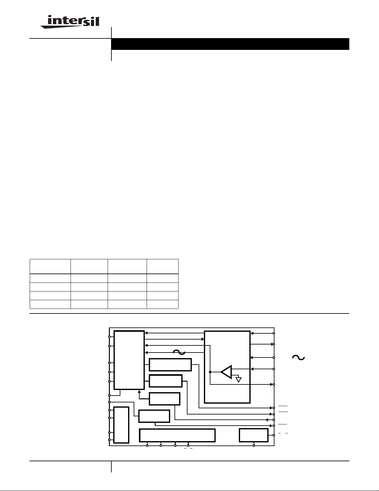
Block Diagram
RING SENSE 1
RING SENSE 2
TIP FEED
TIP SENSE
RING FEED
V
REF
RTI
V
BAT
V
CC
AGND
BGND
60
2-WIRE
INTERFACE
BIAS
V
4-WIRE
INTERFACE
LOOP CURRENT
DETECTOR
FAULT
DETECTOR
CURRENT
LIMIT
RING TRIP
DETECTOR
IIL LOGIC INTERFACE
F1 F0 RS
CAUTION: These devices are sensitive to electrostatic discharge; follow proper IC Handling Procedures.
TST RDI
http://www.intersil.com or 407-727-9207 | Copyright © Intersil Corporation 1999
-
+
RELAY
DRIVER
RX
V
TX
V
RING
- IN 1
OUT 1
SHD
ALM
I
LMT
RTD
RDO
Page 2

HC5517
Absolute Maximum Ratings T
Maximum Supply Voltages
(VCC) . . . . . . . . . . . . . . . . . . . . . . . . . . . . . . . . . . . . .-0.5V to +7V
(VCC)-(V
Relay Drivers . . . . . . . . . . . . . . . . . . . . . . . . . . . . . . . .-0.5V to +15V
) . . . . . . . . . . . . . . . . . . . . . . . . . . . . . . . . . . . . . .90V
BAT
Operating Conditions
Operating Temperature Range
HC5517IM, HC5517IB . . . . . . . . . . . . . . . . . . . . . . -40oC to 85oC
HC5517CM, HC5517CB . . . . . . . . . . . . . . . . . . . . . . 0oC to 75oC
Relay Drivers . . . . . . . . . . . . . . . . . . . . . . . . . . . . . . . . .+5V to +12V
Positive Power Supply (VCC). . . . . . . . . . . . . . . . . . . . . . . +5V ±5%
Negative Power Supply (V
CAUTION: Stresses above those listed in “Absolute Maximum Ratings” may cause permanent damage to the device. This is a stress only rating and operationofthe
device at these or any other conditions above those indicated in the operational sections of this specification is not implied.
NOTES:
1. θJA is measured with the component mounted on an evaluation PC board in free air.
2. All grounds (AGND, BGND) must be applied before VCCor V
to run separate grounds off a line card, the AG must be applied first.
) . . . . . . . . . . . . . . . . . . .-16V to -80V
BAT
Electrical Specifications Unless Otherwise Specified, Typical Parameters are at T
PARAMETER TEST CONDITIONS MIN TYP MAX UNITS
=25oC Thermal Information
A
Thermal Resistance (Typical, Note 1) θJA(oC/W)
PLCC . . . . . . . . . . . . . . . . . . . . . . . . . . . . . . . . . . . . 55
SOIC . . . . . . . . . . . . . . . . . . . . . . . . . . . . . . . . . . . . 70
Maximum Junction Temperature Plastic . . . . . . . . . . . . . . . . .150oC
Maximum Storage Temperature Range. . . . . . . . . . -65oC to 150oC
Maximum Lead Temperature (Soldering 10s) . . . . . . . . . . . . .300oC
(SOIC, PLCC - Lead Tips Only)
Die Characteristics
Transistor Count. . . . . . . . . . . . . . . . . . . . . . . . . . . . . . . . . . . . . .224
Diode Count. . . . . . . . . . . . . . . . . . . . . . . . . . . . . . . . . . . . . . . . . .28
Die Dimensions . . . . . . . . . . . . . . . . . . . . . . . . . . . . . . . . . 174 x 120
Substrate Potential. . . . . . . . . . . . . . . . . . . . . . . . . . . . . . . . . . .V
Process . . . . . . . . . . . . . . . . . . . . . . . . . . . . . . . . . . . . . . .Bipolar-DI
ESD (Human Body Model) . . . . . . . . . . . . . . . . . . . . . . . . . . . .500V
. Failure to do so may result in premature failure of the part. If a user wishes
BAT
Operating TemperatureRange, V
at 600Ω 2-Wire terminating impedance.
= -24V,VCC= +5V,AGND = BGND = 0V. All AC Parametersare specified
BAT
= 25oC, Min-Max Parameters are over
A
BAT
RINGING TRANSMISSION PARAMETERS
Input Impedance (Note 3) - 5.4 - kΩ
V
RING
4-Wire to 2-Wire Gain V
AC TRANSMISSION PARAMETERS
RX Input Impedance 300Hz to 3.4kHz (Note 3) - 108 - kΩ
TX Output Impedance 300Hz to 3.4kHz (Note 3) - - 20 Ω
4-Wire Input Overload Level 300Hz to 3.4kHz R
2-Wire Return Loss Matched for 600Ω (Note 3)
SRL LO 26 35 - dB
ERL 30 40 - dB
SRL HI 30 40 - dB
2-Wire Longitudinal to Metallic Balance
Off Hook
4-Wire Longitudinal Balance Off Hook 300Hz to 3400Hz (Note 3) 50 55 - dB
Low Frequency Longitudinal Balance I
Longitudinal Current Capability I
Insertion Loss 0dBm at 1kHz, Referenced 600Ω
2-Wire/4-Wire (Includes external transhybrid
amplifier with a gain of 3)
to Vt-r (Note 3) - 40 - V/V
RING
= 1200Ω, 600Ω Reference
(Note 3)
Per ANSI/IEEE STD 455-1976 (Note 3)
300Hz to 3400Hz
= 40mA TA = 25oC (Note 3) - 10 23 dBrnC
LINE
= 40mA TA = 25oC (Note 3) - - 40 mA
LINE
L
+1.0 - - V
58 63 - dB
- ±0.05 ±0.2 dB
PEAK
RMS
4-Wire/2-Wire - ±0.05 ±0.2 dB
4-Wire/4-Wire (Includes external transhybrid
amplifier with a gain of 3)
--±0.25 dB
61
Page 3

HC5517
Electrical Specifications Unless Otherwise Specified, Typical Parameters are at T
Operating TemperatureRange, V
= -24V,VCC= +5V,AGND = BGND = 0V. All AC Parametersare specified
BAT
= 25oC, Min-Max Parameters are over
A
at 600Ω 2-Wire terminating impedance. (Continued)
PARAMETER TEST CONDITIONS MIN TYP MAX UNITS
Frequency Response 300Hz to 3400Hz (Note 3) Referenced to
- ±0.02 ±0.06 dB
Absolute Level at 1kHz, 0dBm Referenced 600Ω
Level Linearity Referenced to -10dBm (Note 3)
2-Wire to 4-Wire and 4-Wire to 2-Wire +3 to -40dBm - - ±0.08 dB
-40 to -50dBm - - ±0.12 dB
-50 to -55dBm - - ±0.3 dB
Absolute Delay (Note 3)
2-Wire/4-Wire 300Hz to 3400Hz - - 1.0 µs
4-Wire/2-Wire 300Hz to 3400Hz - - 1.0 µs
4-Wire/4-Wire 300Hz to 3400Hz - 0.95 1.5 µs
Transhybrid Loss V
Total Harmonic Distortion
2-Wire/4-Wire, 4-Wire/2-Wire, 4-Wire/4-Wire
Idle Channel Noise
2-Wire and 4-Wire
= 1V
IN
Reference Level 0dBm at 600Ω
300Hz to 3400Hz (Note 3)
(Note 3)
C-Message
at 1kH (Notes 3, 4) 30 40 dB
P-P
- - -50 dB
- 3 - dBrnC
Psophometric (Note 3) - -87 - dBmp
Power Supply Rejection Ratio (Note 3)
to 2-Wire 20 40 - dB
V
CC
to 4-Wire 20 40 - dB
V
CC
to 2-Wire 20 40 - dB
V
BAT
to 4-Wire 20 50 - dB
V
BAT
to 2-Wire (Note 3)
V
CC
to 4-Wire 20 28 - dB
V
CC
to 2-Wire 20 50 - dB
V
BAT
to 4-Wire 20 50 - dB
V
BAT
30Hz to 200Hz, RL = 600Ω
30 40 - dB
200Hz to 16kHz, RL = 600Ω
DC PARAMETERS
Loop Current Programming
Limit Range 20
-60mA
(Note 5)
Accuracy 10 - - %
Loop Current During Power Denial R
= 200Ω - ±4 ±7mA
L
Fault Currents
TIP to Ground (Note 3) -30-mA
RING to Ground - 120 - mA
TIP and RING to Ground (Note 3) - 150 - mA
Switch Hook Detection Threshold -1215mA
Ring Trip Comparator Voltage Threshold -0.28 -0.24 -0.22 V
Thermal
ALARM Output (Note 3) Safe Operating Die Temperature Exceeded 140 - 160
o
C
62
Page 4

HC5517
Electrical Specifications Unless Otherwise Specified, Typical Parameters are at T
Operating TemperatureRange, V
= -24V,VCC= +5V,AGND = BGND = 0V. All AC Parametersare specified
BAT
= 25oC, Min-Max Parameters are over
A
at 600Ω 2-Wire terminating impedance. (Continued)
PARAMETER TEST CONDITIONS MIN TYP MAX UNITS
Dial Pulse Distortion (Note 3) - 0.1 0.5 ms
Uncommitted Relay Driver
On Voltage V
OL
IOL (RDO) = 30mA - 0.2 0.5 V
Off Leakage Current - ±10 ±100 µA
TTL/CMOS Logic Inputs (F0, F1, RS,
Logic ‘0’ V
Logic ‘1’ V
Input Current (F0, F1, RS,
Input Current (F0, F1, RS,
IL
IH
TST, RDI) IIH, 0V ≤ VIN≤ 5V - - -1 µA
TST, RDI) IIL, 0V ≤ VIN≤ 5V - - -100 µA
TST, RDI)
0 - 0.8 V
2.0 - 5.5 V
Logic Outputs
Logic ‘0’ V
Logic ‘1’ V
OL
OH
Power Dissipation On Hook V
Power Dissipation Off Hook V
I
= 800µA - 0.1 0.5 V
LOAD
I
= 40µA 2.7 - - V
LOAD
CC
V
CC
CC
= +5V, V
= +5V, V
= +5V, V
= -80V, R
BAT
= -48V, R
BAT
= -24V, R
BAT
= ∞ - 300 - mW
LOOP
= ∞ - 150 - mW
LOOP
LOOP
= 600Ω,
- 280 - mW
IL = 25mA
I
CC
I
BAT
VCC = +5V, V
= +5V, V
V
CC
= +5V, V
V
CC
= -80V, R
BAT
= -48V, R
BAT
= -24V, R
BAT
VCC = +5V, VB- = -80V, R
= +5V, VB- = -48V, R
V
CC
= +5V, VB- = -24V, R
V
CC
= ∞ -36mA
LOOP
= ∞ -25mA
LOOP
= ∞ - 1.9 4 mA
LOOP
= ∞ - 3.6 7 mA
LOOP
= ∞ - 2.6 6 mA
LOOP
= ∞ - 1.8 4 mA
LOOP
UNCOMMITTED OP AMP PARAMETERS
Input Offset Voltage - ±5-mV
Input Offset Current - ±10 - nA
Differential Input Resistance (Note 3) - 1 - MΩ
Output Voltage Swing (Note 3) R
= 10kΩ - ±3-V
L
P-P
Small Signal GBW (Note 3) - 1 - MHz
NOTES:
3. These parameters are controlled by design or process parameters and are not directly tested. These parameters are characterized upon initial
design release, upon design changes which would affect these characteristics, and at intervals to assure product quality and specification compliance.
4. For transhybrid circuit as shown in Figure 10.
5. Application limitation based on maximum switch hook detect limit and metallic currents. Not a part limitation.
63
Page 5
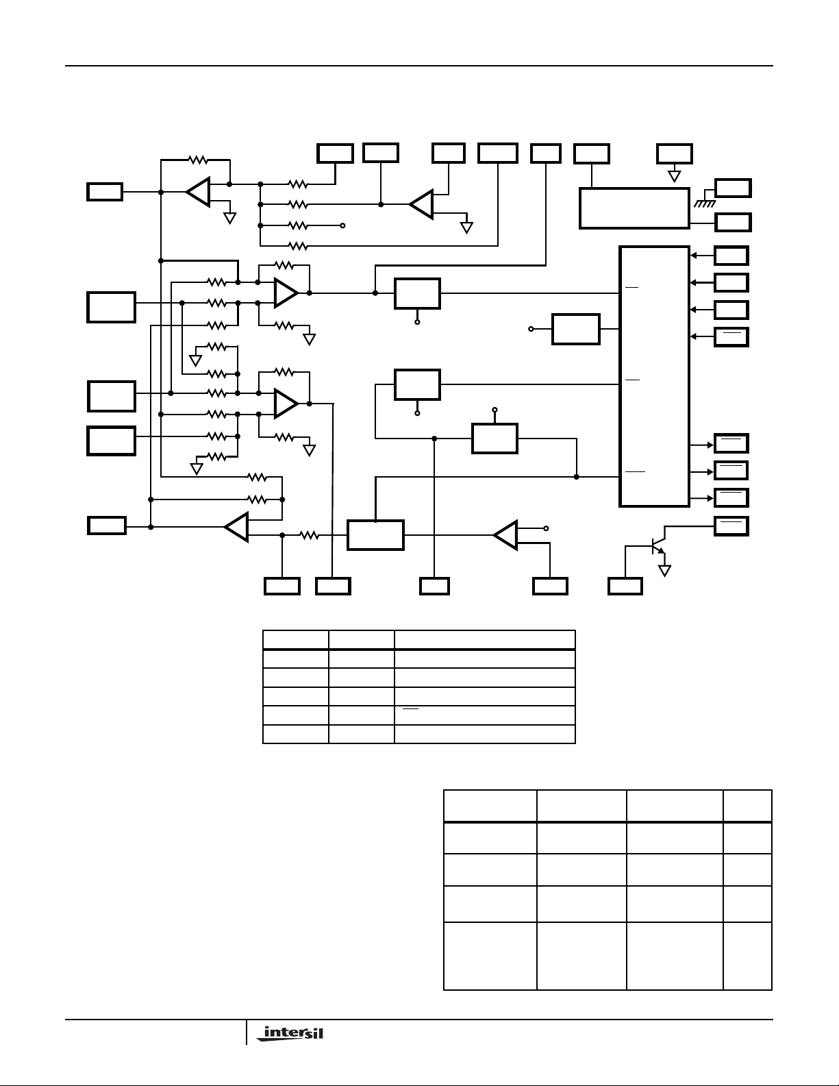
Functional Diagram
HC5517
PLCC/SOIC
TF
TIP
SENSE
RING
SENSE 1
RING
SENSE 2
RF
R
TF
25
14
15
16
26
-
+
100K
100K
100K
100K
R
R
R
R
4.5K
4.5K
RF
2R
-
+
2R
25K
-
+
25K
90K
90K
-
+
VRX
R
R
R/2
R/20
TA
RA
90K
OUT 1
17 12
+2V
VB/2
REF
SHD
RTD
-
+
-IN 1
OP AMP
V
RING
13 24 19 2
FAULT
DET
GM
V
+
TX
THERM
LTD
RF2
V
CC
BIAS
NETWORK
SH
TSD
GK
RFC
AGND
IIL LOGIC INTERFACE
1
22
BGND
27
V
BAT
4
F1
5
F0
6
RS
9
TST
7
SHD
8
RTD
10
ALM
21
RDO
R = 108kΩ
V
REF
3
18
HC5517 TRUTH TABLE
F1 F0 ACTION
0 0 Loop power Denial Active
0 1 Power Down Latch RESET
0 1 Power on RESET
10
1 1 Normal Loop feed
Over Voltage Protection and Longitudinal Current
Protection
The SLIC device, in conjunction with an external protection
bridge, will withstand high voltage lightning surges and
power line crosses.
High voltage surge conditions are as specified in Table 1.
The SLIC will withstand longitudinal currents up to a
maximum or 30mA
RMS
, 15mA
per leg, without any
RMS
performance degradation
.
28
RTINU ILMT
RD Active
PARAMETER
Longitudinal
Surge
Metallic Surge 10µs Rise/
T/GND 10µs Rise/
R/GND
50/60Hz Current
T/GND 11 Cycles 700 (Plastic) V
R/GND Limited to
11
TABLE 1.
TEST
CONDITION
10µs Rise/
1000µs Fall
1000µs Fall
1000µs Fall
10A
RMS
20
RDI
PERFORMANCE
(MAX) UNITS
±1000 (Plastic) V
±1000 (Plastic) V
±1000 (Plastic)
PEAK
PEAK
PEAK
RMS
64
Page 6
HC5517
Circuit Operation and Design Information
The HC5517 is a voltage feed current sense Subscriber Line
Interface Circuit (SLIC). This means that for long loop appli-
cations the SLIC provides a constant voltage to the tip and
ring terminals while sensing the tip to ring current. For short
loops, where the loop current limit is exceeded, the tip to ring
voltage decreases as a function of loop resistance.
The following discussion separates the SLIC’s operation into
its DC and AC path, then follows up with additional circuit
design and application information.
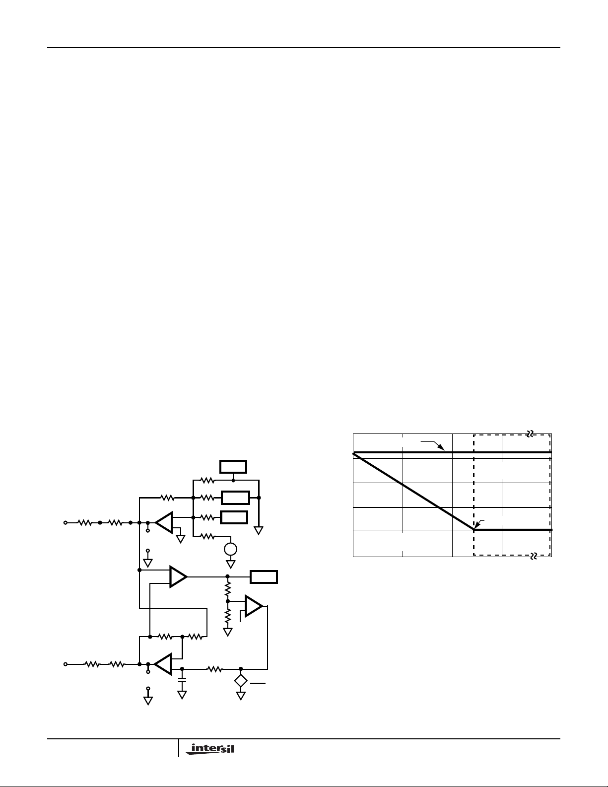
DC Operation of Tip and Ring Amplifiers
SLIC in the Active Mode
The tip and ring amplifiers are voltage feedback op amps
that are connected to generate a differential output (e.g. if tip
sources 20mA then ring sinks 20mA). Figure 1 shows the
connection of the tip and ring amplifiers. The tip DC voltage
is set by an internal +2V reference, resulting in -4V at the
output. The ring DC voltage is set by the tip DC output voltage and an internal V
at the output. (See Equation 1, Equation 2 and Equation 3.)
V
TIPFEEDVC
V
RINGFEEDVD
==
/2 reference, resulting in V
BAT
R
-----------
2V–
R2⁄
V
BAT
-------------- -
2
4V–== =
R
1
V
--- -+
–
R
TIPFEED
R
--- -
R
BAT
(EQ. 1)
(EQ. 2)
+4V
Current Limit
The tip feed to ring feed voltage (Equation 1 minus
Equation 3) is equal to the battery voltage minus 8V. Thus,
with a 48 (24) volt battery and a 600Ω loop resistance,
including the feed resistors, the loop current is 66.6mA
(26.6mA). On short loops the line resistance often
approaches zero and the need exists to control the
maximum DC loop current.
Current limiting is achieved by a feedback network (Figure 1)
that modifies the ring feed voltage (V
) as a function of the
D
loop current. The output of the Transversal Amplifier (TA) has
a DC voltage that is directly proportional to the loop current.
This voltage is scaled by R
and R28. The scaled voltage is
10
the input to a transconductance amplifier (GM) that
compares it to an internal reference level. When the scaled
voltage exceeds the internal reference level, the
transconductance amplifier sources current. This current
charges C
voltage (V
effectively reduces the tip feed to ring feed voltage (V
in the positive direction causing the ring feed
16
) to approach the tip feed voltage (VC). This
D
T-R
and holds the maximum loop current constant.
The maximum loop current is programed by resistors R
10
and R28as shown in Equation 4 (Note: R10is typically
100kΩ).
I
LIMIT
0.6()R10R28+()
---------------------------------------------=
()
200xR
28
(EQ. 4)
),
V
RINGFEEDVDVBAT
R
TIP
RING
V
, V
OUT1
GROUNDED FOR
DC ANALYSIS
R
11
R
RX
13
R
14
12
4+==
R
TIP FEED
-
+
-
V
C
+
TRANSVERSAL
AMP
90kΩ 90kΩ
RING FEED
-
+
+
V
D
-
(EQ. 3)
V
RX
R
R
OUT1
R/20
V
RING
R/2
INTERNAL
+
-
+2V REF
TA
-
+
R
10
R
28
90kΩ
C
16
RF2
V
TX
GM
-
+
V
-
BAT
+
2
FIGURE 1. OPERATION OF THE TIP AND RING AMPLIFIERS
0
V
TIP FEED
-5
-10
-15
-20
TIP AND RING VOLTAGE (V)
-25
CURRENT LIMIT
REGION I
0
FIGURE 2. V
Figure 2 illustrates the relationship between V
= -4V
= 25mA
LOOP
250
LOOP RESISTANCE (Ω)
vs RL(V
T-R
CONSTANT VOLTAGE
V
RING FEED
500 750
= -24V, I
BAT
LIMIT
REGION
= 25mA)
T-R
= -20V
∞
and the
loop resistance. The conditions are shown for a battery voltage of -24V and the loop current limit set to 25mA. For a infinite loop resistance both tip feed and ring feed are at -4V
and -20V respectively. When the loop resistance decreases
from infinity to about 640Ω the loop current (obeying Ohm’s
Law) increases from 0mA to the set loop current limit. As the
loop resistance continues to decrease, the ring feed voltage
approaches the tip feed voltage as a function of the programed loop current limit (Equation 4).
65
Page 7

HC5517
AC Voltage Gain Design Equations
The HC5517 uses feedback to synthesize the impedance at
the 2-wire tip and ring terminals. This feedback network
defines the AC voltage gains for the SLIC.
The 4-wire to 2-wire voltage gain (V
feedback loop shown in Figure 3. The feedback loop senses
the loop current through resistors R
voltage drop and multiplies it by 2 to produce an output voltage at the V
pin equal to +4RS∆IL. The VTXvoltage is
TX
then fed into the -IN1 input of the SLIC’s internal op amp.
This signal is multiplied by the ratio R
tip current summing node via the OUT1 pin. (Note: the internal V
/2 reference (ring feed amplifier) and the internal
BAT
+2V reference (tip feed amplifier) are grounded for the AC
analysis.)
The current into the OUT1 pin is equal to:
I
OUT1
=
4RSIL∆
--------------------–
R
R
8
-------
R
9
Equation 6 is the node equation for the tip amplifier summing
node. The current in the tip feedback resistor (I
Equation 7.
4RSIL∆
--------------------
I
–
–
R
I
–
R
The AC voltage at V
R
4RSIL∆
--------------------
R
R
8
-------
R
9
R
8
-------
R
9
V
RX
-----------+ 0=
R
V
RX
-----------+=
R
is then equal to:
C
to VTR) is set by the
RX
and R14, sums their
13
and fed into the
8/R9
) is given in
R
(EQ. 5)
(EQ. 6)
(EQ. 7)
Substituting the expressions for V
R
∆
SIL
8
-------
R
9
VRX+
24– R
×
I
∆
L
--------------------------------------------------------------------------=
++++
R
LR11R12R13R14
and VD:
C
(EQ. 12)
Equation 12 simplifies to:
2V
400 IL∆–
RX
I
----------------------------------------=
∆
L
Solving for ∆I
V
RX
I
∆
-----------=
L
600
800
results in:
L
(EQ. 13)
(EQ. 14)
Equation 14 is the loop current with respect to the feedback
network. From this, the 4-wire to 2-wire and the 2-wire to
4-wire AC voltage gains are calculated. Equation 15 shows
the 4-wire to 2-wire AC voltage gain is equal to one.
V
RX
-----------
A
4W 2W–
V
TR
-----------
V
RX
I∆
()
LRL
-------------------- -
V
RX
600()
600
--------------------------- 1== = =
V
RX
(EQ. 15)
Equation 16 shows the 2-wire to 4-wire AC voltage gain is
equal to negative one-third.
R
A
2W 4W–
V
OUT1
-------------------
V
TR
-------
∆
4– R
SIL
R
-------------------------------------
I∆LRL()
8
9
V
RX
-----------
200–
600
----------------------------------
V
RX
-----------
600()
600
1()
1
-- -–== = =
3
(EQ. 16)
V
()R()=
CIR
R
8
V
4– RSIL∆
C
-------
R
9
+=
V
and the AC voltage at V
R
8
VD4RSIL∆
The values for R
-------
–=
R
9
V
RX
and R9are selected to match the
8
RX
is:
D
(EQ. 8)
(EQ. 9)
(EQ. 10)
impedance requirements on tip and ring, for more
information reference AN9607 “Impedance Matching Design
Equations for the HC5509 Series of SLICs”. The following
loop current calculations will assume the proper R
and R
8
values for matching a 600Ω load.
∆I
The loop current (
is calculated in Equations 11 through 14. Where R
R
= 40kΩ, RL = 600Ω, R11 = R12 = R13 = R14 = 50Ω.
9
IL∆
--------------------------------------------------------------------------=
++++
R
LR11R12R13R14
) with respect to the feedback network,
L
–
V
CVD
= 40kΩ,
8
(EQ. 11)
Impedance Matching
The feedback network, described above, is capable of
synthesizing both resistive and complex loads. Matching the
SLIC’s 2-wire impedance to the load is important to maximize power transfer and minimize the 2-wire return loss. The
2-wire return loss is a measure of the similarity of the impedance of a transmission line (tip and ring) and the impedance
at it’s termination. It is a ratio, expressed in decibels, of the
power of the outgoing signal to the power of the signal
reflected back from an impedance discontinuity.
Requirements for Impedance Matching
Impedance matching of the HC5517 application circuit to the
9
transmission line requires that the impedance be matched to
points “A” and “B” in Figure 3. T o do this, the sense resistors
R
11,R12,R13
and R14must be accounted for by the feedback network to make it appear as if the output of the tip and
ring amplifiers are at points “A” and “B”. The feedback network
takes a voltage that is equal to the voltage drop across the
sense resistors and feeds it into the summing node of the tip
amplifier. The effect of this is to cause the tip feed voltage to
become more negative by a value that is proportional to the
voltage drop across the sense resistors R
and R13. At the
11
same time the ring amplifier becomes more positive by the
66
Page 8

HC5517
R
R
R/20
R/2
4– RSIL∆
V
OUT1
V
RING
4– RSIL∆()
----------------------------- -
I
R
+
TIP
A
V
TR
R
∆V
-
∆I
L
L
+
IN
-
+
∆I
L
-
+
B
RING
R
V
8
RX
-------
------------ -+=
R
R
R
9
∆I
R
R
∆I
∆I
+
L
L
-
11
12
L
+-
-
R
13
R11 = R12 = R13 = R14 = R
R
14
∆I
L
-
+
I
R
R
-
+
-
V
C
+
90kΩ 90kΩ
-
+
+
V
D
-
V
C
S
VD4RSIL∆
RX
R
8
-------
R
9
-
+
+
-
R
8
-------
R
9
VRX+=
+RS∆I
-RS∆I
VRX–=
1V
P
4RS∆I
R
L
I
OUT1
=
2R
8
R
9
†
+
2V
DC
-
L
R
+
2
V
-
L
TX
+
4RS∆I
-
9
-IN
L
R
8
-
1
+
-
R
4RS∆I
8
L
R
9
+
†
V
-
BAT
+
2
† GROUNDED FOR AC ANALYSIS
FIGURE 3. AC VOLTAGE GAIN AND IMPEDANCE MATCHING
same amount to account for resistors R12 and R14.
The net effect cancels out the voltage drop across the feed
resistors. By nullifying the effects of the feed resistors the
feedback circuitry becomes relatively easy to match the
impedance at points “A” and “B”.
IMPEDANCE MATCHING DESIGN EQUATIONS
Matching the impedance of the SLIC to the load is
accomplished by writing a loop equation starting at V
going around the loop to V
impedance of any load is as follows (Note: V
. The loop equation to match the
C
RX
and
D
= 0 for this
analysis):
R
8
-------
R
9
2R
SILVIN
R
8
------ -
R
9
R
8
-------
R
9
∆–∆+
R
-------
R
4R
4R
++=
8
9
∆ RLIL∆++=
SIL
SRL
+
0=+
(EQ. 17)
(EQ. 18)
(EQ. 19)
4RSIL∆–
RLIL∆ 2RSIL∆ 4RSIL∆–
V
∆ 8RSIL∆–
IN
VIN∆ IL∆ 8RS–
(-8R
S(R8/R9
VIN∆
------------- 8– R
∆
I
L
)) and the loop impedance (+4RS+RL).
R
8
-------
4RSR
++=
S
R
9
L
(EQ. 20)
The result is shown in Equation 20. Figure 4 is a schematic
representation of Equation 15.
R
L
∆V
LOAD
+
IN
-
SLIC
8RS
R
8
-------
R
9
4RS+
FIGURE 4. SCHEMATIC REPRESENTATION OF EQUATION 20
To match the impedance of the SLIC to the impedance of the
load, set:
R
8
RL8R
If R
9
-------
4RS+=
S
R
9
is made to equal 8RS then:
RLR84RS+=
(EQ. 21)
(EQ. 22)
Equation 19 can be separated into two terms, the feedback
67
Page 9

HC5517
Therefore to match the HC5517, with RSequal to 50Ω,toa
600Ω load:
R98RS850Ω()400Ω== =
(EQ. 23)
and:
R8RL4– RS600Ω 200Ω– 400Ω== =
To prevent loading of the V
output, the value of R8and R
TX
(EQ. 24)
are typically scaled by a factor of 100:
KR840kΩ= KR940kΩ=
(EQ. 25)
Since the impedance matching is a function of the voltage
gain, scaling of the resistors to achieve a standard value is
recommended.
For complex impedances the above analysis is the same.
KR940kΩ= KR8100 Resistive 200–()
Reactive
--------------------------+=
100
(EQ. 26)
Reference application note AN9607 (“Impedance Matching
Design Equations for the HC5509 Series of SLICs”) for the
values of KR
and KR8for several worldwide Typical line
9
impedances.
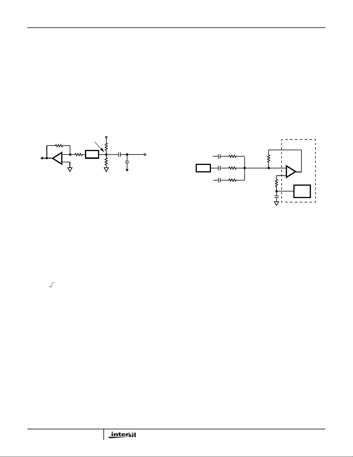
Tip-to-Ring Open-Circuit Voltage
The tip-to-ring open-circuit voltage, VOC, of the HC5517 is
programmable to meet a variety of applications. The design
of the HC5517 defaults the value of V
V
OCVBAT
8–≅
The HC5517 application circuit overrides the default V
operation when operating from a -80V battery. While operating from a -80V battery, the SLIC will be in either the ringing
mode or on-hook standby mode. In the ringing mode, V
designed to switch from 0V (centering voltage) to -47V
(Maintenance Termination Unit voltage). The centering voltage is active during the ringing portion of the ringing waveform and the Maintenance TerminationUnit (MTU) voltage is
active during the silent portion of the ringing signal. In the
on-hook standby mode, the application circuit is designed to
maintain V
at the MTU voltage.
OC
Centering Voltage Application Circuit Overview
The centering voltage is used during ringing to center the
DC outputs of the tip feed and ring feed amplifiers. Centering
the amplifier outputs allows for the maximum undistorted
voltage swing of the ringing signal. Without centering, the
output of each amplifier would saturate at ground or V
minimizing the ringing capability of the HC5517. The
required centering voltage, V
, is +1.8VDCwhen operating
C
from a -80V battery.
Centering Voltage Application Circuit Operation
The circuit used to generate the centering voltage is shown
in Figure 5.
OC
to:
OC
BAT
OC
is
+5V
+
-
V
-----------------
BAT
R
19
T
2
TO ZENER
DIODE D
V
2
RING
11
V
C
D
13
D
6
R
18
R
24
RC
9
TF
RF
FIGURE 5. CENTERING VOLTAGE APPLICATION CIRCUIT
R R/20
-
+
TIP FEED
AMPLIFIER
90kΩ 90kΩ
-
+
RING FEED
AMPLIFIER
R/2
+2V
90kΩ
The circuitry within the dotted lines is internal to the
HC5517. The value of the resistor designated as R is 108kΩ
and the resistor R/20 is 5.4kΩ. The tip amplifier gain of
20V/V amplifies the +1.8V
the internal 4V
offset, generating -40VDCat the tip
DC
amplifier output. The -40V
at VCto +36VDCand adds it to
DC
offset also sums into the ring
DC
amplifier, adding to the battery voltage, achieving -40V at the
ring amplifier output.
Centering Voltage Design Equations
The centering voltage (V
voltage. A battery voltage of -80V requires a +1.8V
) is dependent on the battery
C
DC
centering voltage. The equation used to calculate the
centering voltage is shown below.
V
V
BAT
-------------- -
C
2
4–
20⁄=
(EQ. 27)
The DC voltage at the outputs of the centered tip and ring
amplifiers can be calculated from Equation 28 and
Equation 29.
V
,
V
20VC4+()–=
TC
RCVBAT
20VC4+()+=
The shunt resistor of the divider network, R
(EQ. 28)
(EQ. 29)
, is not
18
determined from a design equation. It is selected based on
the trade-off of power dissipation in the voltage divider (low
value of R
(high value of R
) and loading affects of the internal R/20 resistor
18
). The suggested range of R18is between
18
1.0kΩ and 2.0kΩ. The application circuit design equation
used to calculate the value of R
of the divider network is
19
as follows:
68
Page 10

HC5517
R
19
where: V
VCCV
----------------------------------------------------------------------------------------------------=
V
R
R
V
V
D13VD6VC
+()RINVCR
V
CVD6
forward drop of D13, 0.63V.
D13
forward drop of D6, 0.54V.
D6
is the shunt resistor of the divider, 1.1kΩ.
18
is the input impedance of V
IN
is the required centering voltage, 1.8V,V
C
is the +5V supply.
CC
–––()R18RIN•()
+
18
, 5.4kΩ.
RING
BAT
(EQ. 30)
= -80V.
Centering Voltage Logic Control
The pnp transistor T2is used to defeat the voltage divider
formed by R
high), +5V
19,R18,D13
is divided to produce +1.8VDCat the V
DC
and D6. When T2is off (RC is logic
RING
input. When T2is on (RC is logic low), its emitter base voltage of +0.9V
D
, hence reverse biasing the diode (D6) and floating the
6
V
pin.
RING
is divided resulting in +0.2V at the anode of
DC
MTU Voltage Application Circuit Overview
According to Bellcore specification TR-NWT-000057, an
MTU voltage may be required by some operating
companies. The minimum allowable voltage to meet MTU
requirements is -42.75V, which is used by measurement
equipment to verify an active line. Also, some facsimile and
answering machines use the MTU voltage as an indication
that the telephone is on-hook or not answered. In addition to
the Bellcore specification, FCC Part 68.306 requires that the
maximum tip to ground or ring to ground voltage not exceed
-56.5V for hazardous voltage limitations. These two requirements have been combined and the resulting range is
defined as the MTU voltage. The HC5517 application circuit
can be programmed to any voltage within this range using
the zener clamping circuit.
MTU Voltage Application Circuit Operation
The circuit used to generate the MTU voltage is shown in
Figure 6.
90K 90K
RF
RING FEED
AMPLIFIER
FIGURE 6. RING FEED AMPLIFIER CIRCUIT CONNECTIONS
-
+
V
3
REF
C
16
The ring feed amplifier DC output voltage, V
function of the internal V
diode D
. When the magnitude of V
11
/2 reference and external zener
BAT
TIP FEED OUTPUT
90K
D
11
V
BAT
----------------2
R
19
/2 is less than the
BAT
+5V
T
2
RDC
R
24
RC
,isa
zener voltage, the zener is off and the input to the ring feed
amplifier is V
/2. When the magnitude of V
BAT
BAT
/2 is
greater than the zener voltage, the zener conducts and
clamps the noninverting terminal of the ring amplifier to the
zener voltage.
Internal to the HC5517 are connections to the tip feed amplifier
output and V
output, V
TDC
/2 reference. The DC voltage at the tip feed
BAT
, is a constant -4V during on-hook standby.
MTU Voltage Design Equations
The following equations are used to predict the DC output of
the ring feed amplifier, V
V
BAT
-------------- -
V
-------------- -
Where V
V
VZ< V
2
BAT
VZ≥ V
2
Z
are the saturation voltages of T2. Using Equations 31
BE
RDC
RDC
is the zener diode voltage of D11and VCEand
.
RDC
V
BAT
-------------- -
2
2
2V–
ZVCEVBE
4+=
–()+()4+=
(EQ. 31)
(EQ. 32)
and 32, the tip-to-ring open-circuit voltage can be calculated
for any value of zener diode and battery voltage.
V
BAT
2
BAT
2
VZ< V
VZ≥ V
-------------- -
V
-------------- -
Figure 7 plots V
OCVTDC
OCVTDC
as a function of battery voltage. The
OC
V
BAT
-------------- -
2
2
2V–
ZVCEVBE
4––=
–()+()4––=
(EQ. 33)
(EQ. 34)
graph illustrates the clamping function of the zener circuitry.
+50
+40
+30
+20
TIP TO RING
+10
OPEN CIRCUIT VOLTAGE (V)
0
-16 -28 -40 -52 -58 -68 -80
FIGURE 7. VOC AS A FUNCTION OF BATTERY VOLTAGE
MTU Voltage Logic Control
The same pnp transistor, T
, that is used to control the
2
centering voltage is also used to control the MTU voltage.
The application circuit uses T
of the zener diode D
anode of D
is referenced to ground through the collector
11
. When RC is a logic low (T2on) the
11
to ground or float the anode
2
base junction of the transistor. Current then flows through
the zener, allowing the ring amplifier input to be clamped.
When RC is a logic high (T
off) the anode of D11floats,
2
inhibiting the clamping action of the zener.
HC5517 Modes of Operation
The four modes of operation of the HC5517 Ringing SLIC
are ringing, on-hook standby, off-hook active and power
denial. Three control signals select the operating mode of
69
Page 11

HC5517
the SLIC. The signals are Battery Switch, F1 and Ring
Cadence (RC). The active application circuit and active
supervisory function are different for each mode, as shown
in the Table 2.
Mode Control Signals
The Battery Switch selects between the -80V and -24V
supplies. The Battery Switch circuitry is described in the
“Operation of the Battery Switch” section. A system alternative to the battery switch signal is to use a buffered version of
the
SHD output to select the battery voltage. Another alternative is to control the output of a programmable battery
supply, removing the battery switch entirely from the application circuit. F1 is used to put the SLIC in the power denial
mode. RC drives the base of T
, which is the transistor used
2
to control the centering voltage and MTU voltage. The three
control signals can be driven from a TTL logic source or an
open collector output
RINGING MODE
The ringing state, as the name indicates, is used to ring the
telephone with a -80V battery supply. The SLIC is designed
for balanced ringing with a differential gain of 40V/V across tip
and ring. Voltage feed amplifiers operating in the linear mode
are used to amplify the ringing signal. The linear amplifier
approach allows the system designer to define the shape and
amplitude of the ringing waveform. Both supervisory function
outputs,
SHD and RTD, are active during ringing.
Spectral Content of the Ringing Signal
The shape of the waveform can range from sinusoidal to
trapezoidal. Sinusoidal waveforms are spectrally cleaner
than trapezoidal waveforms, although the latter does result
in lower power dissipation across the SLIC for a given RMS
amplitude. Systems where the ringing signal will be in proximity to digital data lines will benefit from the sinusoidal ringing capability of the HC5517. The slow edge rates of a
sinusoid will minimize coupling of the large amplitude ringing
signal. The linear amplifier architecture of the HC5517
allows the system designer to optimize the design for power
dissipation and spectral purity.
Amplitude of the Ringing Signal
Amplitude control is another benefit of the linear amplifier
architecture. Systems that require less ringing amplitude are
able to do so by driving the HC5517 with a lower level ringing
waveform. Solutions that use saturated amplifiers can only
vary the amplitude of the ringing signal by changing the
negative battery voltage to the SLIC.
HC5517 Through SLIC Ringing
The HC5517 is designed with a high gain input, V
the system drives while ringing the phone. V
RING
, that
RING
is one of
many signals summed at the inverting input to the tip feed
amplifier. The gain of the V
signal through the tip feed
RING
amplifier is set to 20V/V. The output of the tip feed amplifier
is summed at the inverting input of the ring feed amplifier,
configured for unity gain. The result is a differential gain of
40V/V across tip and ring of the ringing signal.
The ringing function requires an input ringing waveform and
a centering voltage. The ringing waveform is the signal from
the 4-wire side that is amplified by the SLIC to ring the telephone. The centering voltage, as previously discussed, is a
positive DC offset that is applied to the V
RING
input along
with the ringing waveform. The HC5517 application circuit
provides the centering voltage, simplifying the system
interface to an AC coupled ringing waveform.
Ringer Equivalence Number
Before any further discussion, the Ringer Equivalence
Number or REN must be discussed. Based on FCC Part
68.313 a single REN can be defined as 5kΩ,7kΩ or 8kΩ of
AC impedance at the ringing frequency. The ringing frequency is based on the ringing types listed in Table 1 of the
FCC specification. The impedance of multiple REN is the
paralleling of a single REN. Therefore 5 REN can either be
1kΩ, 1.4kΩ or 1.6kΩ. The 7kΩ model of a single REN will be
used throughout the remainder of the data sheet.
Ringing Waveform
An amplitude of 1.2V
to a 1 REN load, and 42V
will deliver approximately 46V
RMS
to a 3 REN load. The ampli-
RMS
RMS
tude is REN dependent and is slightly attenuated by the
feedback scheme used for impedance matching. The ringing
waveform is cadenced, alternating between a 20Hz burst
and a silent portion between bursts. Bellcore specification
TR-NWT-000057 defines seven distinct ringing waveforms or
alerting (ringing) patterns. The following table lists each type.
TABLE 1. DISTINCTIVE ALERTING PATTERNS
INTERVAL DURATION IN SECONDS
P ATTERN
RINGING SILENT RINGING SILENT RINGING SILENT
A 0.4 0.2 0.4 0.2 0.8 4.0
B 0.2 0.1 0.2 0.1 0.6 4.0
C 0.8 0.4 0.8 0.4
D 0.4 0.2 0.6 4.0
E 1.2 4.0
F1±0.2 3 ± 0.3
G 0.3 0.2 1.0 0.2 0.3 4.0
Figure 8 shows the relationship of the cadenced ringing
waveform and the Battery Switch and RC control signals.
Also shown are the states of the MTU voltage and the
centering voltage.
The state of Battery Switch is indicated by the desired
battery voltage to the SLIC. The RC signal is used to enable
and disable the centering voltage and MTU voltage. RC
follows the ring signal in that it is high during the 20Hz burst
and low during the static part of the waveform.
Open Circuit Voltage During the Ringing Mode
The mutually exclusive relationship of the centering voltage
and MTU implies that both functions will not exist at the
same time. During the silent portion of the ringing waveform
70
Page 12

HC5517
CADENCED
WAVEFORM
RC
MTU
-80V
-24V
OFF ON OFF OFF OFFON ON
ON OFF ON ON ONOFF OFF
BATTERY
SWITCH
CENTERING
VOLTAGE
FIGURE 8. RINGING WAVEFORM AND CONTROL SIGNALS
the HC5517 application circuit meets the hazardous voltage
requirements of FCC Part 68.306 by forcing the MTU voltage. Without the zener clamping solution, a programmable
power supply would have to be designed. The intervals listed
in Table 1 would require the power supply to switch voltages
and settle to stable operation well within 100ms. The design
of such a power supply may prove quite a challenge. The
zener solution provides a cost effective, low impact to
meeting a wide variety of tip to ring open circuit voltages.
Ringing Design Equations
The differential tip to ring voltage during ringing, as a
function of REN, can be approximated from Equation 35.
VTRRL()2
The voltage V
V
------------------
5.4e3
RING
input ringing signal. V
ential output voltage, calculated as V
0.702()200()V
RING
---------------------------------------------------–×≅ 108e3•
108e3()R
TRO
L
is defined as the RMS amplitude of the
is the open circuit tip to ring differ-
TRO
multiplied by the
RING
(EQ. 35)
differential gain of 40V/V. The REN impedance is shown as
R
. Figure 9 shows the relationship of REN load to maxi-
L
mum differential tip to ring RMS voltage during ringing. The
maximum ringing signal amplitude herein assumes an infinite source and sink capability of the tip feed and ring feed
amplifiers. Due to the amplifier output design, the HC5517 is
limited to 3 REN ringing capability for this reason.
47.00
46.00
45.00
44.00
43.00
42.00
41.00
AMPLITUDE (RMS)
MAXIMUM RINGING
40.00
39.00
1 REN 2 REN 3 REN 4 REN 5 REN
FIGURE 9. MAXIMUM RINGING OUTPUT VOLTAGE
(V
RING
= 1.2V
RMS
)
ON-HOOK STANDBY MODE
On-hook standby mode is with the phone on-hook (i.e., not
answered) and ready to accept an incoming voice signal or electronic data. The HC5517 application circuit is designed to maintain the MTU voltage during this mode of operation. During this
mode, the
SHD output is valid and the RTD output is invalid.
OFF-HOOK ACTIVE MODE
Off-hook active accommodates voice and data communications, including pulse metering, with a batter y voltage of
-24V. The MTU voltage dur ing this mode is defeated by the
zener clamp design regardless of the state of RC. It is
important to have RC low to disable the ringing voltage.
Only the
SHD output is valid during this mode.
POWER DENIAL MODE
The HC5517 will enter the power denial mode whenever F1
is a logic low. During power denial, the tip and ring amplifiers
are active. The DC voltages of both amplifiers are near
ground, resulting in a maximum loop current of 7mA. Both
the
SHD and the RTD detector output are invalid.
71
Table 2 summarizes the operating modes of the HC5517
application circuit. The table indicates the valid detectors in
each mode as well as valid application circuit operation.
Page 13

HC5517
TABLE 2. HC5517 APPLICATION CIRCUIT OPERATING MODES SUMMARY
BATTERY
SWITCH F1 RC MODE
-24V 0 0 Power Denial
-24V 0 1 Invalid
-24V 1 0 Off-Hook Active √
-24V 1 1 Invalid
-80V 0 0 Power Denial √
-80V 0 1 Invalid
-80V 1 0 On-Hook Standby √√
-80V 1 1 Ringing (Note) √√
NOTE: During Ringing, the SHD output will be active for both on-hook and off-hook conditions. The AC current, for the on-hook condition, exceeds
the SHD threshold of 12mA. Valid off-hook detection during ringing is provided by the RTD output only.
DETECTORS VALID APPLICATION CIRCUIT VALID
SHD RTD MTU CENTERING
Operation of the Battery Switch
The battery switch is used to select between the off-hook
battery of -24V and the ringing/standby battery of -80V.
When T
is off and the -24V battery is supplied to the SLIC through
D
10
flows through the collector of T
When D
respect to the drain (-80V) and T
connects the -80V battery to the SLIC through D
turn reverse biases D
Transhybrid Balance
The purpose of the transhybrid circuit is to remove the
receive signal (V-REC) from the transmit signal (V-XMIT),
thereby preventing an echo on the transmit side. This is
accomplished by using an external op amp (usually part of
the CODEC) and by the inversion of the signal from the
SLIC’s 4-wire receive port (V
transmit port (OUT1).
The external transhybrid circuit is shown in Figure 10. The
effects of capacitors C
fore omitted from the analysis. The input signal (V-REC) will
be subtracted from the output signal (V-XMIT) if I
are equal and opposite in phase. A node analysis yields the
following equation:
VREC–
-------------------- -
The value of R
R
2
Given that OUT1 is equal to -1/3 of V-REC (Equation 16) and
V-REC is equal to VTR (A
then R
be achieved by using 1% resistors values.
is off (battery switch is logic low) the MOSFET T
1
. When T1is on (battery switch is logic high) current
turning on the zener D9.
turns on, the gate of the MOSFET is positive with
9
, isolating the two supplies.
10
1
turns on. Turning T3on
3
7
. This in
(Voice Signal)
) to the SLIC’s 4-wire
RX
and C8are negligible and there-
5,C7
equals I
1
OUT1
---------------- -+ 0=
R
R
2
3
is then:
2
V REC–
-------------------- -
R–
•=
3
OUT1
=3R3.A transhybrid balance greater than 30dB can
2
4-Wire-2-Wire
= 1, Equation 15),
(EQ. 36)
(EQ. 37)
EXTERNAL
HC5517
3
PHASE
SHIFT
OF AC
SIGNAL
FIGURE 10. TRANSHYBRID CIRCUIT (VOICE SIGNAL)
V
RX
C
-
+
180
8
-IN1
OUT1
SUMMING NODE CANCELS OUT
INCOMING AC TRANSMISSION FROM
OUT GOING TRANSMISSION
Transhybrid Balance
TRANSHYBRID CIRCUIT
C
7
C
5
R
9
R
8
I
1
R
2
R
3
I
2
(Pulse Metering)
V-REC
INCOMING
AC TRANSMISSION
R
1
-
+
V-XMIT
OUTGOING
AC TRANSMISSION
Transhybrid balance of the pulse metering signal is
accomplished in 2 stages. The first stage uses the SLIC’s
2
internal op amp to invert the phase of the pulse metering signal. The second stage sums the inverted pulse metering signal with the incoming signal for cancellation in the
transhybrid amplifier. A third network can be added to offset
both tip and ring by the peak amplitude of the pulse metering
signal. This will allow both the maximum voice and pulse
metering signals to occur at the same time with no distortion.
Pulse Metering
Pulse metering or Teletax is used outside the United States
for billing purposes at pay phones. A 12kHz or 16kHz burst
is injected into the 4-wire side of the SLIC and transmitted
across the tip and ring lines from the central office to the pay
phone. For more information about pulse metering than covered here reference application note AN9608 “Implementing
Pulse Metering for the HC5509 Series of SLICs”.
72
Page 14

HC5517
Inverting Amplifier (A1)
The pulse metering signal is injected in the -IN1 pin of the
SLIC. This pin is the inverting input of the internal amplifier
(A
) that is used to invert the pulse metering signal for later
1
cancellation. The components required for pulse metering
are C
and R5, are shown in Figure 11. The pulse metering
6
signal is AC coupled to prevent a DC offset on the input of
the internal amplifier. The value of C
should be 10µF. The
6
expression for the voltage at OUT1 is given in Equation 38.
C6R
C
8
DESIGN
R
-------
• V
R
5
-IN
PM
R
8
1
-
+
R
8
-------
•–=
R
5
R
9
8
9
V
PM
V
TX
FIGURE 11. PULSE METERING PHASE SHIFT AMPLIFIER
V
OUT1
VTX–
A
1
TO EXTERNAL
TRANSHYBRID AMP
OUT
1
(EQ. 38)
The first term is the gain of the feedback voltage from the
2-wire side and the second term is the gain of the injected
pulse metering signal. The effects of C
and C8are
6
negligible and therefore omitted from the analysis.
The injected pulse metering output term of Equation 38 is
shown below in Equation 39 and rearranged to solve for R
in Equation 40.
V
R
OUT1
=
5R8
injected()V
The ratio of R
8
-------
• 1==
PM
R
5
to R5is set equal to one and results in unity
8
(EQ. 39)
(EQ. 40)
R
gain of the pulse metering signal from 4-wire side to 2-wire
side. The value of R
is considered to be a constant since it
8
is selected based on impedance matching requirements.
Cancellation of the Pulse Metering Signal
The transhybrid cancellation technique that is used for the
voice signal is also implemented for pulse metering. The
technique is to drive the transhybrid amplifier with the signal
that is injected on the 4-wire side, then adjust its level to
match the amplitude of the feedback signal, and cancel the
signals at the summing node of an amplifier.
NOTE: The CA741C operational amplifier is used in the application
as a “stand in” forthe operational amplifier that is traditionally located
in the CODEC, where transhybrid cancellation is performed.
Referring to Figure 3, VTXis the 2-wire feedback used to
drive the internal amplifier (A1) which in turn drives the
OUT1 pin of the SLIC. The voltage measured at V
TX
related to the loop impedance as follows:
200–
------------ -
V
TX
VPM• GPM•=
R
L
(EQ. 41)
For a 600Ω termination and a pulse metering gain (G
1, the feedback voltage (V
) is equal to one third the
TX
PM
)of
injected pulse metering signal of the 4-wire side. Note,
depending upon the line impedance characteristics and the
degree of impedance matching, the pulse metering gain may
differ from the voice gain. The pulse metering gain (G
PM
)
must be accounted for in the transhybrid balance circuit.
The polarity of the signal at OUT1 (Equation 38) is opposite
of V
allowing the circuit of Figure 12 to perform the final
PM
stage of transhybrid cancellation.
R
V
RX
OUT
V
PM
FIGURE 12. CANCELLATION OF THE PULSE METERING SIGNAL
2
R
3
1
R
4
R
1
-
+
CA741C
V
TXO
The following equations do not require much discussion.
They are based on inverting amplifier design theory. The
voice path V
signal has been omitted for clarity. All refer-
RX
ence designators refer to components of Figures 11 and 12.
V
TXO
V
V
TX
R–
•
8
PM
---------- -–
------------–
R
• V
5
R
9
R
-------
R
1
–=
3
R
PM
1
-------
•
R
4
(EQ. 42)
The first term refers to the signal at OUT1 and the second
term refers to the 4-wire side pulse metering signal. Since
5
ideal transhybrid cancellation implies V
TXO
when a signal is injected on the 4-wire side, V
equals zero
is set to
TXO
zero and the resulting equation is shown below.
0R
8
TX
---------- -
•
------------+
R
R
9
PM
5
1
-------
• V
–=
R
3
R
V
V
Rearranging terms of Equation 43 and solving for R
R
PM
1
-------
•
R
4
(EQ. 43)
results
4
in Equation 44. This is the only value to be calculated for the
transhybrid cancellation. All other values either exist in the
application circuit or have been calculated in previous
sections of this data sheet.
R
200– GPM•
8
-------
R
=
4
The value of R
------------------------------- -
•
R
3
•
R
LR9
(Figure 12) is 12.37kΩ given the following
4
1–
1
-------+
R
5
(EQ. 44)
set of values:
R
= 40kΩ
8
R
= 40kΩ
9
R
= 600Ω
L
R
= 8.25kΩ
3
R
= 40kΩ
5
G
= 1
PM
is
Substituting the same values into Equation 41 and Equation 42,
it can be shown that the signal at OUT
This result, along with Equation 44 where R
is equal to -2/3VPM.
1
equals to 2/3R4,
3
indicates the signal levels into the transhybrid amplifier are
equalized by the amplifier gains and opposite in polarity,
thereby achieving transh ybrid balance at V
TXO
.
73
Page 15
HC5517
Additional Tip and Ring Offset Voltage
A DC offset is required to level shift tip and ring from ground
and V
respectively. By design, the tip amplifier is offset
BAT
4V below ground and the ring amplifier is offset 4V above
V
. The 4V offset was designed so that the peak voice
BAT
signal could pass through the SLIC without distortion. Therefore, to maintain distortion free transmission of pulse metering and voice, an additional offset equal to the peak of the
pulse metering signal is required.
The tip and ring voltages are offset by a voltage divider
network on the V
pin. The VRXpin is a unity gain input
RX
designed as the 4-wire side voice input for the SLIC.
Figure 13 details the circuit used to generate the additional
offset voltage.
+5V
R
-
2-WIRE SIDE
FIGURE 13. PULSE METERING OFFSET GENERATION
+
V
PMO
R
V
RX
R
6
C
7
R
7
TO VOICE INPUT OF
TRANSHYBRID AMP
4-WIRE SIDE
C
VOICE INPUT
5
The amplifier shown is the tip amplifier. Other signals are connected to the summing node of the amplifier but only those
components used for the offset generation are shown. The offset generated at the output of the tip amplifier is summed at the
ring amplifier inverting input to provide a positive offset from the
battery voltage. The connection to the ring amplifier was omitted from Figure 13 for clarity, refer to Figure 3 for details.
The term V
is defined to be the offset required for the
PMO
pulse metering signal. The value of the offset voltage is calculated as the peak value of the pulse metering signal.
Equation 45 assumes the amplitude of the pulse metering
signal is expressed as an RMS voltage.
V
PMO
The value of R
2VPM•=
can be calculated from the following
6
(EQ. 45)
equation:
R
=
6
R7R
----------------- -
R
7
–
5V
PMO
------------------------- -
R+
V
PMO
(EQ. 46)
The component labeled R is the internal summing resistor of
the tip amplifier and has a typical value of 108kΩ. The value
of R
should be selected in the range of 4.99kΩ and 10kΩ.
7
Staying within these limits will minimize the parallel loading
effects of the internal resistor R on R
as well as minimize
7
the constant power dissipation introduced by the divider.
Solving Equation 45 for 1V
requirement for V
. Setting R7of Equation 46 to 10kΩ
PMO
and substituting the values for V
R
. The value of R6can be rounded to the nearest standard
6
results in a 1.414V
RMS
and R yields 23.2kΩ for
PMO
value without significantly changing the offset voltage.
Single Low Voltage Supply Operation
The application circuit shown Figure 15 requires 2 low
voltage supplies (+5V, -5V). The following application offers
away to make use of a 2.5V reference, provided with some
CODEC, to operate the transhybrid balance amplifier from
a single +5V supply. The implementation is shown in
Figure 14. Notice that the three inputs from the SLIC must all
be AC coupled to insure the proper DC gain through the
CODECs internal op amp. The resistor Ra is not used for
gain setting and is only intended to balance the DC offsets
generated by the input bias current of the CODEC amplifier.
If the DC offsets generated by the input bias currents are
negligible, then Ra may be omitted from the circuit. Ca may
be required for decoupling of the voltage reference pin and
does not contribute to the response of the amplifier.
CODEC
R
0.1µF
V
RX
0.1µF
OUT
1
0.1µF
V
PM
FIGURE 14. SINGLE LOW VOLTAGE SUPPLY OPERATION
2
R
3
R
4
R
24.9kΩ
24.9kΩ
1
Ra
Ca
0.1µF
+
2.4V
REF
Layout Guidelines and Considerations
The printed circuit board trace length to all high impedance
nodes should be kept as short as possible. Minimizing length
will reduce the risk of noise or other unwanted signal pickup.
The short lead length also applies to all high gain inputs. The
set of circuit nodes that can be categorized as such are:
•V
pin 27, the 4-wire voice input.
RX
• -IN1 pin 13, the inverting input of the internal amplifier.
•V
•V
• U1 pin 2, inverting input of external amplifier.
For multi layer boards, the traces connected to tip should not
cross the traces connected to ring. Since they will be carrying
high voltages, and could be subject to lightning or surge
depending on the application, using a larger than minimum
trace width is advised.
The 4-wire transmit and receive signal paths should not
cross. The receive path is any trace associated with the V
input and the transmit path is any trace associated with V
output. The physical distance between the two signal paths
should be maximized to reduce crosstalk.
The mode control signals and detector outputs should be
routed away from the analog circuitry. Though the digital
signals are nearly static, care should be taken to minimize
coupling of the sharp digital edges to the analog signals.
pin 3, the noninverting input to ring feed amplifier.
REF
pin 24, the 20V/V input for the ringing signal
RING
RX
TX
74
Page 16

HC5517
The part has two ground pins, one is labeled AGND and the
other BGND. Both pins should be connected together as
close as possible to the SLIC. If a ground plane is available,
then both AGND and BGND should be connected directly to
the ground plane.
A ground plane that provides a low impedance return path
for the supply currents should be used. A ground plane
provides isolation between analog and digital signals. If the
layout density does not accommodate a ground plane, a
single point grounding scheme should be used.
Application Pin Descriptions
PLCC SYMBOL DESCRIPTION
1 AGND Analog Ground - To be connected to zero potential. Serves as a reference for the transmit output and receive input
terminals.
2VCCPositive Voltage Source - Most Positive Supply.
3V
4 F1 PowerDenial -A low activeTTL compatiblelogic control input. When enabled, the output of the ring amplifier will ramp
5 F0 TTL compatible logic control input that must be tied high for proper SLIC operation.
6 RS TTL compatible logic control input that must be tied high for proper SLIC operation.
7 SHD Switch Hook Detection - An active low TTL compatible logic output. Indicates an offhook condition.
8 RTD Ring Trip Detection - An active low TTL compatible logic output. Indicates an off-hook condition when the phone is
9 TST A TTL logic input. A low on this pin will keep the SLIC in a power down mode. The TST pin in conjunction with the ALM pin
10 ALM A TTL compatible active low output which responds to the thermal detector circuit when a safe operating die
11 I
12 OUT1 The analog output of the spare operational amplifier.
13 -IN1 The inverting analog input of the spare operational amplifier. Note that the non-inverting input of the amplifier is
14 TIP
15 RING SENSE 1 An analog input connected to the RING (more negative) side of the subscriber loop through a feed resistor. Functions
16 RING SENSE 2 This is an internal sense mode that must be tied to RING SENSE 1 for proper SLIC operation.
17 V
18 NU Not used in this application.This pin should be left floating.
19 V
20 RDI TTL compatible input to drive the uncommitted relay driver.
21 RDO This is the output of the uncommitted relay driver.
22 BGND Battery Ground - To be connected to zero potential. All loop current and some quiescent current flows into this
23 NU Not used in this application. This pin should be either grounded or left floating.
24 V
25 TF This is the output of the tip amplifier.
26 RF This is the output of the ring amplifier.
27 V
28 RTI Ring Trip Input - This pin is connected to the external negative peak detector output for ring trip detection.
REF
LMT
SENSE
RX
TX
RING
BAT
Ring amplifier referenceoverride.An external voltageconnected tothis pinwill overridethe internal V
close to the output voltage of the tip amplifier.
ringing.
can provide thermal shutdown protection for the SLIC. Thermal shutdown is implemented by a system controller that
monitors the ALM pin. When the ALM pin is active (low) the system controller issues a command to the TST pin (low) to
power down the SLIC. The timing of the thermal recovery is controlled by the system controller.
temperature has been exceeded.
Loop Current Limit - Voltageon this pin sets the short loop current limiting conditions using a resistive voltage divider.
internally connected to AGND.
An analog input connected to the TIP (more positive) side of the subscriber loop through a feed resistor and ring relay
contact. Functions with the RING terminal to receive voice signals from the telephone and for loop monitoring
purpose.
with the TIP terminal to receive voice signals from the telephone and for loop monitoring purposes.
Receive Input, 4-Wire Side - A high impedance analog input. AC signals appearing at this input drive the Tip Feed
and Ring Feed amplifiers deferentially.
Transmit Output, 4-Wire Side-Alowimpedance analog output which represents the differential voltage across TIP
andRING. Since the DC levelof this output varies with loop current, capacitivecoupling to the next stage isnecessary.
terminal.
Ring signal input (0V to 3V
The negative battery source.
PEAK
at 20Hz).
/2 reference.
BAT
75
Page 17

HC5517
Pinouts
HC5517 (PLCC)
TOP VIEW
VREF
F1
4
3
F0
5
RS
6
SHD
7
8
RTD
TST
9
ALM
10
ILMT
11
12
13
14
-IN 1
OUT 1
Applications Circuit
VCCAGND
12
28
15
16
TIP SENSE
RING SENSE 1
BAT
RTI
RF
V
27
26
25
24
23
20
19
17
18
RX
NU
V
RING SENSE 2
22
21
TF
VRING
NU
BGND
RDO
RDI
V
TX
1
1
AGND
2
2
V
CC
3
3
VREF
F1
4
4
F0
5
5
RS
6
6
SHD
7
7
RTD
8
8
TST
9
9
ALM
10
10
11
11
ILMT
OUT 1
12
12
-IN 1
13
13
14
TIP SENSE
+5V
14
PULSE METERING OPTION
HC5517 (SOIC)
TOP VIEW
28
28
RTI
27
27
V
BAT
26
26
RF
25
25
TF
24
24
VRING
23
23
NU
BGND
22
22
RDO
21
21
20
20
RDI
V
19
19
TX
NU
18
18
17
17
V
RX
16
16
RING SENSE 2
15
15
RING SENSE 1
R
TIP
RING
V
CC
BAT
SWITCH
BGND
-24V
-80V
11
R
C
17
D
2
C
9
D
4
††
C
18
R
22
D
10
R
14
R
12
C
15
D
12
T
1
C
13
D
7
T
3
†D
R
21
D
9
14 TIP SENSE
13
25 TF
D
1
V
BAT
D
3
26 RF
16 RING SENSE 2
15 RING SENSE 1
2 V
CC
C
14
1 AGND
22 BGND
C
12
27 V
BAT
8
SHD RTD ALM TST RS
† Not required for MOSFETs with body diodes.
†† Diode bridge optional for in-house use.
HC5517
V
ILIMT 11
V
-IN1 13
OUT1 12
VR
RDI 20
RDO
V
RING
R
29
17
RX
TX
F1 4
FO 5
EF
24
RTI 28
+5V
R
6
C
7
V-REC
R
C
1
R
7
R
28
R
10
19
C
8
R
9
R
8
R
3
R
5
5
R
2
U1
2
R
3
4
C
1
7
6
-
+
4
C
6
-5V+5V
C
2
C
C
4
3
V-XMIT
V-TELETAX
F1
R
31
+5V
3
D
13
21
691087
R
30
D
6
R
18
R
16
R
15
C
D
5
R
17
C
10
+5V
R
R
24
19
T
2
RC
11
D
11
C
16
V
RING
76
FIGURE 15. APPLICATION CIRCUIT
Page 18

HC5517
HC5517EVAL Evaluation Board Parts List
COMPONENT VALUE TOLERANCE RATING COMPONENT VALUE TOLERANCE RATING
SLIC HC5517 n/a n/a C2, C4, C
R1, R
2
R
3
R
4
R5, R8, R
9
R6(Not Provided) 23.2kΩ 1% 1/4W C
R7(Not Provided) 10kΩ 1% 1/4W C
R
10
R
11-14
R
15
R
16
R
17
R
18
R
19
24.9kΩ 1% 1/4W C5, C
8.25kΩ 1% 1/4W C6, C
12.1kΩ 1% 1/4W C9, C
40kΩ 1% 1/4W C
100kΩ 5% 1/4W C
50Ω 1% 1/4W C17, C
47kΩ 1% 1/4W D
7
8
12
10
11
13
16
18
, D7, D8, D
1-4
1.5MΩ 1% 1/4W D5, D6, D12, D
56.2kΩ 1% 1/4W D
1.1kΩ 1% 1/4W D
825Ω 1% 1/4W T
9
11
1
15
0.1µF 20% 50V
10µF 20% 20V
0.47µF 20% 20V
0.01µF 20% 100V
1.0µF 20% 50V
100µF 20% 5V
0.1µF 20% 100V
0.5µF 20% 50V
3300pF 20% 100V
1N4007 100V, 1A
10
1N914 100V, 1A
13
1N4744 15V, 1W
1N5255 28V, 1/2-
NTE 383 100V, 1A
Wire
R22, R29, R30, R
R
24
10kΩ 5% 1/4W T
31
47kΩ 5% 1/4W T
2
3
2N2907 60V,150mA
RFP2N10 or
100V, 2A
equivalent
R
25-27
R
28
R
21
C1, C3, C
14
560Ω 5% 1/4W F1, RC, BATTERY SPDT Toggle switches, center off.
20kΩ Potentiometer 1/4W U1 CA741C OpAmp
47kΩ 5% 1/4W Textool Socket 228-5523
0.01µF 20% 50V
All Intersil semiconductor products are manufactured, assembled and tested under ISO9000 quality systems certification.
Intersil semiconductor products are sold by description only.Intersil Corporation reserves the right to make changes in circuit design and/or specifications at any time without notice. Accordingly,the reader is cautioned to verify that data sheets are current before placing orders. Information furnished by Intersil is believed to be accurate and
reliable. However, no responsibility is assumed by Intersil or its subsidiaries for its use; nor for any infringements of patents or other rights of third parties which may result
from its use. No license is granted by implication or otherwise under any patent or patent rights of Intersil or its subsidiaries.
For information regarding Intersil Corporation and its products, see web site http://www.intersil.com
Sales Office Headquarters
NORTH AMERICA
Intersil Corporation
P. O. Box 883, Mail Stop 53-204
Melbourne, FL 32902
TEL: (407) 724-7000
FAX: (407) 724-7240
EUROPE
Intersil SA
Mercure Center
100, Rue de la Fusee
1130 Brussels, Belgium
TEL: (32) 2.724.2111
FAX: (32) 2.724.22.05
ASIA
Intersil (Taiwan) Ltd.
7F-6, No. 101 Fu Hsing North Road
Taipei, Taiwan
Republic of China
TEL: (886) 2 2716 9310
FAX: (886) 2 2715 3029
77
 Loading...