

Page 1

查询HC1-5504DLC-5供应商
®
N
E
M
M
O
C
E
R
May 1997
T
O
N
c
r
o
1
e
e
S
t
c
a
t
n
o
N
I
-
8
8
8
-
0
5
5
C
H
e
T
r
u
o
L
I
S
R
E
T
S
N
G
I
S
E
D
W
E
N
R
O
F
D
E
D
B
4
n
h
c
r
o
C
H
d
n
a
i
w
p
u
S
l
a
c
n
i
.
w
w
1
B
4
0
5
5
p
e
t
n
e
C
t
r
o
m
o
c
.
l
i
s
r
HC-5504DLC
t
a
r
e
t
c
s
t
/
SLIC
Subscriber Line Interface Circuit
Features
• Pin for Pin Replacement for the HC-550 4
• Capable of +5V or +12V (
VB+) Operation
• Monolithic Integrat ed Device
• DI High Voltage Process
• Compatible With Worldwide PBX Performance
Requirements
• Controlled Supply of Battery Feed Current for Short
Loops (41mA)
• Internal Ring Relay Driver
• Allows Interfacing With Negative Superimposed Ringing Systems
• Low Power Consumption During Standby
• Switch Hook Ground Key and Ring Trip Detection
Functions
• Selective Denial of Power to Subscriber Loops
Applications
• Solid State Line Interface Circuit for Analog and Digital PBX Systems
• Direct Inward Dial (DID) Trunks
• Voice Messaging PBXs
• Allows Multi-Phone Operation
Description
The Intersil SLIC incorporates many of the BORSHT functions
on a single IC chip. This includes DC battery feed, a ring relay
driver, supervisory and hybrid functions. This device is
designed to maintain transmissi on performanc e in the pr esence of externally induced longitudinal currents. Using the
unique Intersil d iel e ct ric i s ol a t ion pr o cess, the S LIC can operate directly with a wide range of station battery voltages.
The SLIC also provides selective denial of power. If the PBX
system bec om es overloaded duri ng an emergency, the SLIC
will provide system protection by denying power to selected
subscriber l oops.
The Intersil SLIC is i deally suited for the design of new digital
PBX systems by eliminati ng bulky hybrid transformers.
Ordering Information
PART
NUMBER
HC1-5504DLC-5 0
HC1-5504DLC-9 -40
HC3-5504DLC-5 0
HC3-5504DLC-9 -40
HC4P5504DLC-5 0
HC4P5504DLC-9 -40
HC9P5504DLC-5 0
HC9P5504DLC-9 -40
TEMPERATURE
RANGE PACKAGE
o
to +75oC 24 Lead Ceramic DIP
o
to +85oC 24 Lead Ceramic DIP
o
to +75oC 24 Lead Plastic DIP
o
to +85oC 24 Lead Plastic DIP
o
to +75oC 28 Lead PLC C
o
to +85oC 28 Lead PLC C
o
to +75oC 24 Lead SOIC
o
to +85oC 24 Lead SOIC
Pinouts
HC-5504DLC (PDIP, CDIP, SOIC)
TOP VIEW
TIP
1
RING
2
3
RFS
VB+
4
C3
5
DG
6
RS
7
RD
8
TF
9
RF
10
11
VB-
BG
12
CAUTION: These devic es are sensitive to electrostatic discharge; foll ow prop er IC Handling Pro cedures.
1-888-INTERSIL or 321-724-7143
Copyright © Intersil Americas Inc. 2002. All Rights Reserved
| Intersil (and design) is a registered trademark of Intersil Americas Inc .
TX
24
AG
23
C4
22
21
R
X
+IN
20
19
-IN
OUT
18
C2
17
16
RC
15
PD
14
GKD
13
SHD
VB+
N/C
8-19
C3
DG
RS
RD
TF
HC-5504DLC (PLCC)
TOP VIEW
RING
RFS
4
5
6
7
8
9
10
11
12 13 14 15 16 17 18
RF
TIP
N/C
-
B
BG
V
N/C
TX
AG
C4
262728123
RX
25
+IN
24
-IN
23
N/C
22
OUT
21
C2
20
RC
19
PD
GKD
SHD
File Number 2443.3
Page 2

Specifications HC-5504DLC
Absolute Maximum Ratings (Note 1) Operating C o ndi t io ns
Maximum Continuous Supply Voltages
(V
-) . . . . . . . . . . . . . . . . . . . . . . . . . . . . . . . . . . . . . -60 to +0.5 V
B
(V
+). . . . . . . . . . . . . . . . . . . . . . . . . . . . . . . . . . . . . -0.5 to +15 V
B
(V
+ - VB-) . . . . . . . . . . . . . . . . . . . . . . . . . . . . . . . . . . . . . . +75V
B
Relay Drive Voltage (V
Junction Temperature Ceramic . . . . . . . . . . . . . . . . . . . . . . +175
) . . . . . . . . . . . . . . . . . . . . . . .-0.5 to +15V
RD
Junction Temperature Plastic. . . . . . . . . . . . . . . . . . . . . . . . +150
Lead Temperature (Soldering 10 Sec.) . . . . . . . . . . . . . . . . +300
CAUTION: Stresses above those listed in “Absolute Maximum Ratings” may cause permanent damage to the device. This is a stress only rating and operation
of the device at these or any other conditions above those indicated in the operational sections of this specification is not implied.
Operating Temperature Range
HC-5504DLC-5 . . . . . . . . . . . . . . . . . . . . . . . . . . . . 0
HC-5504DLC-9 . . . . . . . . . . . . . . . . . . . . . . . . . . .-40
Storage Temperature Range . . . . . . . . . . . . . . . . . . -65
Relay Driver Voltage (V
o
Positive Supply Voltage (V
C
o
Negative Supply Voltage (V
C
o
High Level Logic Input Voltage . . . . . . . . . . . . . . . . . . . . . . . . . 2.4V
C
). . . . . . . . . . . . . . . . . . . . . . . +5 to +12V
RD
+). . . . . . . 4.7 5 to 5.25 or 10.8 to 13.2 V
B
-) . . . . . . . . . . . . . . . . . . . . -42 to -58V
B
Low Level Logic Input Voltage . . . . . . . . . . . . . . . . . . . . . . . . . 0.6V
Loop Resistance (R
) . . . . . . . . . . . . . . . . . . . . . . . . . 200 to 1200Ω
L
o
C to +75oC
o
C to +85oC
o
C to 150oC
Electrical Specifications Unless Otherwise Specified, VB- = -48V, VB+ = +12V and +5V, AG = BG = DG = 0V, Typical Parameters
TA = +25oC. Min-Max Parameters are Over Operating Temperature Range.
PARAMETER CONDITIONS MIN TYP MAX UNITS
On Hook Power Dissipation I
Off Hook Power Dissipation R
Off Hook IB+ R
Off Hook IB+ R
Off Hook IB- R
Off Hook Loop Curr ent R
Off Hook Loop Curr ent R
Off Hook Loop Curr ent R
* = 0, VB+ = +12V - 170 235 mW
LONG
= 600Ω, I
L
= 600Ω, I
L
= 600Ω, I
L
= 600Ω, I
L
= 1200Ω, I
L
= 1200Ω, VB- = -42V, I
L
T
= +25oC
A
= 200Ω, I
L
* = 0, VB+ = +12V - 425 550 mW
LONG
* = 0, TA = -40oC--6.0mA
LONG
* = 0, TA = +25oC--5.3mA
LONG
* = 0 - 35 41 mA
LONG
* = 0 - 21 - mA
LONG
* = 0
LONG
* = 0 36 41 48 mA
LONG
17.5 - - mA
Fault Curr en ts
TIP to Ground -14-mA
RING to Ground -55-mA
TIP to RING -41-mA
TIP and RING to Ground -55-mA
Ring Relay Drive V
OL
Ring Relay Driver Off Leakage V
Ring Trip Detection Period R
IOL = 62mA - 0.2 0.5 V
= +12V, RC = 1 = HIGH, TA = +25oC--100µA
RD
= 600Ω -23Ring
L
Cycles
On Hook Ringing Current - - 30 mApk
Switch Hook Detection Threshold SHD
SHD
Ground Key Detection Thresh old GKD
GKD
Loop Current During Power Denial R
= 200Ω - ±2-mA
L
= V
= V
= V
= V
OL
OH
OL
OH
18 - - mA
--12mA
20 - - mA
--10mA
Dial Pulse Distortion 0-5ms
Receive Input Impedance (Note 2) - 110 - kΩ
Transmit Output Impedance (Note 2) - 10 20 Ω
Two Wire R eturn Loss (Referenced to 600Ω + 2.16µF), (Note 2)
LO -15.5- dB
SR
L
ER
L
HI -31-dB
SR
L
Longit udinal Balance 1V
200Hz - 3400Hz, (Note 2) IEEE Method
RMS
-24-dB
2 Wire Off Hook 58 65 - dB
2 Wire On Hook 60 63 - dB
o
4 Wire Off Hook 0
C ≤ TA ≤ +75oC5058-dB
8-20
Page 3

Specifications HC-5504DLC
Electrical Specifications Unless Otherwise Specified, V
TA = +25oC. Min-Max Parameters are Over Operating Temperature Range. (Continued)
- = -48V, VB+ = +12V and +5V, AG = BG = DG = 0V, Typical Parameters
B
PARAMETER CONDITIONS MIN TYP MAX UNITS
Low Freq uency Longitudinal Balance R.E.A. Method, (Note 2), RL = 600Ω
o
0
C ≤ TA ≤ +75oC
--23dBrnC
---67dBm0p
Insertion Loss at 1kHz, 0dBm Input Level, Referenced 600Ω
2 Wire - 4 Wire, 4 Wire - 2 Wire - ±0.05 ±0.2 dB
Frequency Response 200 - 3400Hz Referenced to Absolute Loss at
- ±0.02 ±0.05 dB
1kHz and 0dBm Signal Level (Note 2)
Idle Channel Noise (Note 2)
2 Wire - 4 Wire, 4 Wire - 2 Wire - 1 5 dBrnC
- -89 -85 dBm0p
Absolute Delay (Note 2)
2 Wire - 4 Wire, 4 Wire - 2 Wire - - 2 ms
Trans Hybrid Loss Balance Network Set Up for 600Ω Terminatio n at
36 40 - dB
1kHz
Overload Level V
2 Wire - 4 Wire, 4 Wire - 2 Wire V
+ = +5V 1.5 - - Vpeak
B
+ = +12V 1.75 - - Vpeak
B
Level Li nearity At 1kHz, (N ote 2) Referenced to 0dBm Level
2 Wire - 4 Wire, 4 Wire - 2 Wire +3 to -40dBm - - ±0.05 dB
-40 to -50dBm - - ±0.1 dB
-50 to -55dBm - - ±0.3 dB
Power Supply Rejection Ratio (Note 2)
+ to 2 Wire 30 - 60Hz, RL = 600Ω 15 - - dB
V
B
+ to Tr ansmit 15 - - dB
V
B
- to 2 Wire 15 - - dB
V
B
- to Transmit 15 - - dB
V
B
+ to 2 Wire 200 - 16kHz RL = 600Ω 30 - - dB
V
B
+ to Tr ansmit 30 - - dB
V
B
- to 2 Wire 30 - - dB
V
B
- to Transmit 30 - - dB
V
B
Logic Input Current (RS, RC
, PD)0V ≤ VIN ≤ + 5V - - ±100 µA
Logic Inputs
Logic ‘0 ’ V
Logic ‘1 ’ V
IL
IH
--0.8V
2.0 - 5.5 V
Logic Out puts
I
Logic ‘0 ’ V
Logic ‘1 ’ V
= Longit udinal Current
*I
LONG
OL
OH
800µA, VB+ = +12V, +5V - 0.1 0.5 V
LOAD
I
80µA, VB+ = +12V 2.7 5.0 5.5 V
LOAD
40µA, VB+ = +5V 2.7 - 5.0 V
I
LOAD
NOTES:
1. Absolute maximum ratings are limiting values, applied individually, beyond which the serviceability of the circuit may be impaired. Func-
tional operability und er any of these conditions is not necessarily implied.
2. These para mete rs are con trol led by des ign or process param eters and are no t direc tly test ed. These para mete rs are cha racte rized up on
initia l d esi gn rel ea se, upon des ig n ch an ges w hi ch wo ul d aff ec t these cha r acte r isti cs , a nd a t int erv al s t o as sure pr oduc t q ual i ty and specific ation compliance .
8-21
Page 4
Specifications HC-5504DLC
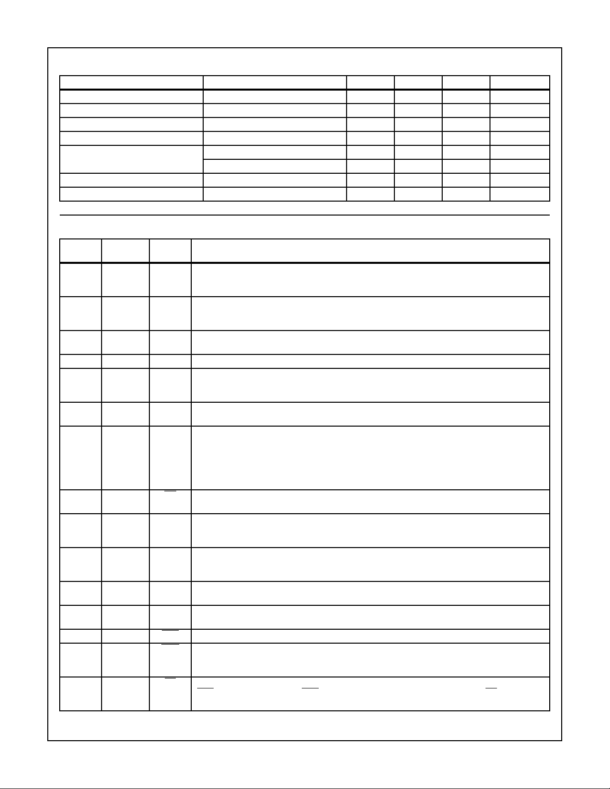
Uncommitted Op Amp Specifications
PARAMETER CONDI TIONS MIN TYP MAX UNITS
Input Offset Volt a ge - ±5- mV
Input Offset Current - ±10 - nA
Input Bias Current - 20 - nA
Differential Input Resistance (Note 2) - 1 - MΩ
Output Voltage Swing R
Output Resistance A
Small Signal GBW (Note 2) - 1 - MHz
= 10K, VB+ = +12V - ±5-V
L
RL = 10K, VB+ = +5V - ±3-V
= 1 (Note 2) - 10 - Ω
VCL
PEAK
PEAK
Pin Descriptions
28 PIN
PLCC
24 PIN
DIP/SOIC SYMBOL DESCRIPTION
2 1 TIP An analog input con ne ct ed to th e TIP (mor e pos itiv e) si de of the sub sc rib er loop thr oug h a 15 0Ω fe ed
resistor and a ring relay contact. Functions with the Ring terminal to receive voice signals from the
telephone and for loop monitoring purposes.
3 2 RING An analog input co nn ected to t he RI NG (more ne gative ) side o f th e subscriber loop t hrough a 1 50 Ω
feed resistor and a ring relay contact. Functions with the Tip terminal to receive voice signals from the
telephone and for loop monitoring purposes.
4 3 RFS Senses ring si de of loo p f or g r ou nd k ey and ri ng tri p d etec t io n. D uri ng ring in g, the ri ng sign al is i ns ert -
ed into the line at this node and RF is isolated fr om RFS via a relay.
54V
+ Positive Voltage Source - Most positive supply. VB+ is typi cally 12V or 5V.
B
6 5 C3 Capacitor #3 - An external capacitor to be connected between this terminal and analog ground.
Requir e d f or p roper ope ration o f the loop cu rr e nt l im it i ng functio n, an d for filtering V
-. Typical value
B
is 0.3µF, 30V.
7 6 DG Digital Ground - To be connected to zero potential and serves as a reference for all digital inputs and
outputs on the SLIC microcircuit.
9 7 RS Ring Synchronization Input - A TTL - compatible clock input. The clock should be arranged such that
a positive pulse transition occurs on the zero crossing of the ring voltage source, as it appears at the
RFS terminal. For Tip side injected systems, the RS pulse should occur on the negative going zero
crossing an d f or Ri ng i nj ecte d s ystem s, on t he po sit i ve go in g z ero cr os sing. T his e ns ur es t ha t th e r ing
relay ac ti vate s and de act iv ates w hen the inst an tane ou s ring vo lt age is near zero. I f syn chro niza tio n
is not required, the pin should be tied to +5V.
10 8 RD
Relay D river - A low active open co llector logic output. When enab led, the externa l ring relay is
energized.
11 9 TF Tip Fe ed - A l ow impe danc e anal og ou tput c onnec ted t o the T IP te rmin al t hrough a 150Ω feed resistor.
Funct ions with the RF te rmin al to pr ov ide lo op cu rre nt, feed v oice sign al s to th e te leph one s et, an d
sink lon gitudin al current.
12 10 RF Ring F ee d - A l ow im peda nce a nalo g ou tput con ne cted to the R IN G te rmin al t hro ugh a 150 Ω feed
resis tor. Func ti ons with the T F t erm inal to p rov ide l oop cur ren t, fe ed voic e si gnal s to the tele ph one
set, and sink longi tudinal current.
13 11 V
- Negative Voltage Source - Most negative supply. VB- is typic ally -48 V wi th an opera tio nal rang e of
B
-42V to -58V. Frequently referred to as “battery”.
14 12 BG Battery Ground - To be connected to zero potential. All loop current and some quiescent current flows
into this ground terminal.
16 13 SHD
17 14 GKD
Switch Hook Detection - A low active LS TTL - compatible logic output.
Ground Key Detection - A low active LS TTL - compatible logic output. This output is enabled if the
DC current into the ring lead exceeds the DC current ou t of the tip lead by more than 20mA, and dis-
abled if this current difference is below an internally set threshold.
18 15 PD
Power Denial - A low active TTL - Compatible logic input. When enabled, the switch hook detect
(SHD
) and ground key detect (GKD) are not necessarily valid, and the relay driver (RD) output is dis -
abled.
8-22
Page 5
Pin Descriptions (Continued)
Specifications HC-5504DLC
28 PIN
PLCC
24 PIN
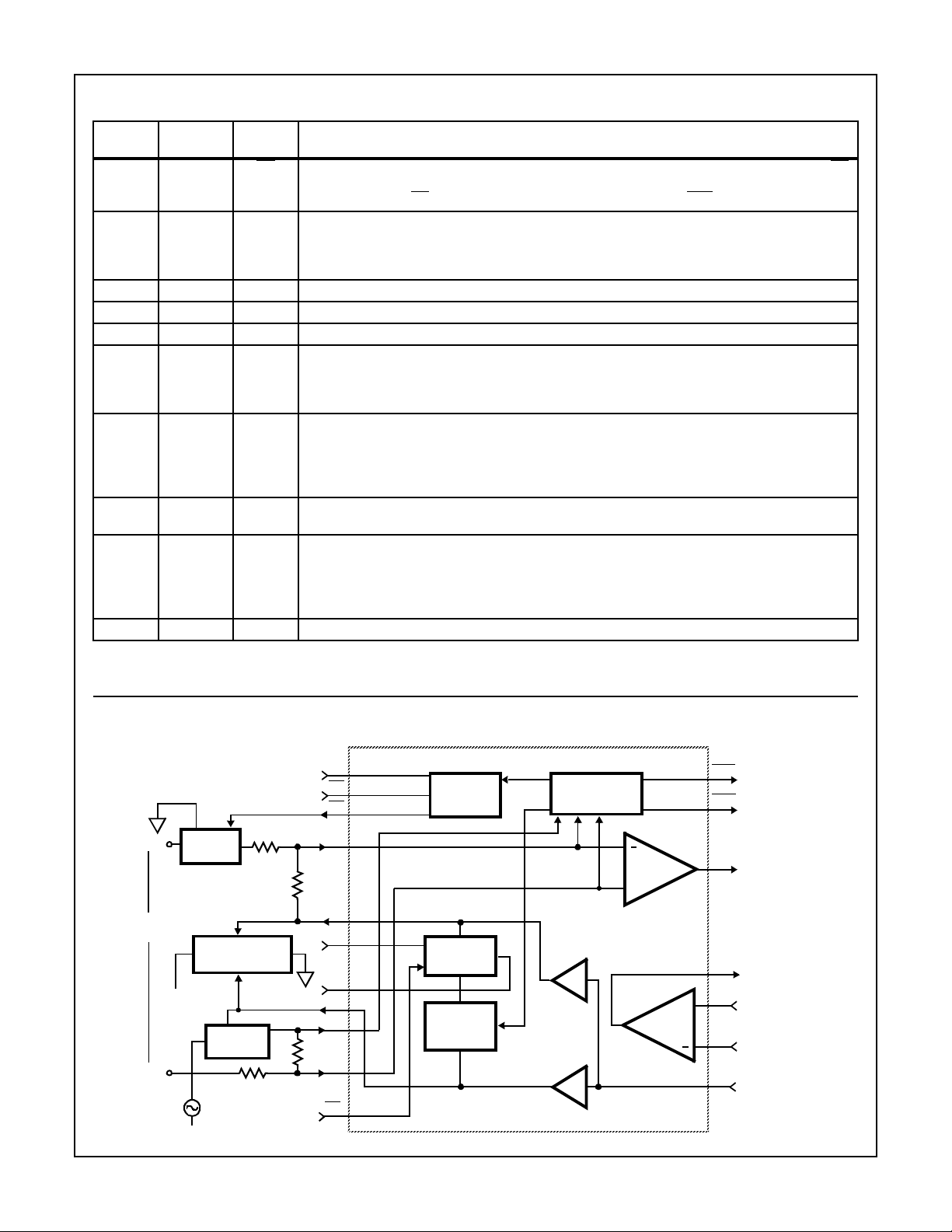
DIP/SOIC SYMBOL DESCRIPTION
19 16 RC Ring Command - A low acti ve TTL - C ompatible logic inp ut. When enabled, the relay driver (R D)
output goes low on the next high level of the ring sync (RS) input, as long as the SLIC is not in the
power denial state (PD
= 0) or the subscriber is not already off- hook (SHD = 0).
20 17 C2 Capacitor #2 - An external capacitor to be connected between this terminal and digital ground.
Prevents false ground key indications from occurring during ring trip detection. Typical value is
0.15µF, 10V . This capacitor is not used if ground key function is not required and (Pin 17) may be l eft
open or co nnecte d to dig ital grou nd.
21 18 OUT The analog output of the spare operational amplifier. The output voltage swing is typically ±5V.
23 19 -IN The inverting analog input of the spare operational amplifier.
24 20 +IN The non-inverting analog input of the spare operational amplifier.
25 21 RX Receive Input, Four Wire Side - A high im pedance analog input w hich is inter nally biased. Capacitive
coupli ng t o t h is inp ut i s re qu ir ed. A C s ig na ls ap pe ar i ng at t h is inp ut d iff er ent ia ll y dri ve th e Ti p fe ed a nd
Ring feed terminals, which in turn drive tip and ring through 300Ω of feed resistance on each side of
the line.
26 22 C4 Capacitor #4 - An external capacitor to be connected between this terminal and analog ground. This
capacitor preven ts false ground ke y indication and false r ing trip dete ction from o ccurring when
longitudinal currents are induced onto the subscriber loop from near by power lines and other noise
sources. This capacitor is also required for the proper operation of ring trip detection. Typical value is
0.5µF, to 1.0µF, 20V. This capacitor should be nonpolarized.
27 23 AG Analog Ground - To be connected to zero potential and se rves as a reference for the transmit output
(TX) and receive input (RX) terminals.
28 2 4 TX Transmi t O utput , Fo ur Wir e Side - A lo w im peda nce a nalo g out put which rep resen ts the di ffe rentia l
voltage across Tip and Ring. Transhybrid balancing must be performed (using the SLIC microcircuit’s
spare op amp ) be yo nd thi s ou tp ut to comp le tel y imp le me nt two to four wire conv er s io n. Thi s ou t put is
unbalanced and referenced to analog ground. Since the DC level of this output varies with loop
current, capacitive coupling to the next stage is essential.
1,8,15,22 NC No Intern al Connection.
NOTE: All grounds (AG, BG, & DG) must be applied before V
wishes to run separate grounds off a lin e card, the AG must be applied first.
+ or VB-. Failure to do so may result in premature failure of the part. If a user
B
Functional Diagram
RING SYNC
RING COMMAND
1/2 RING
TIP
2 WIRE
LOOP
RING
RING
VOLTAGE
VB-
RELAY
SECONDARY
PROTECTION
1/2 RING
RELAY
POWER DENIAL
-
150Ω
150Ω
RFS
150Ω
150Ω
RING
RS
RC
RD
TIP
BG
V
PD
TF
RF
RING
TRIP
RING
CONTROL
BATTERY
-
B
FEED
LOOP
CURRENT
LIMITER
SLIC MICROCIRCUIT
MONITORING
+1
LINE
DRIVERS
-1
LOOP
DIFF
AMP
+
OP
AMP
SHD
SWITCH HOOK
DETECTION
GKD
GROUND KEY
DETECTION
TX
TRANSMIT
OUTPUT
OUT
+IN
+
-IN
RX
RECEIVE
INPUT
8-23
Page 6
Schematic
HC-5504DLC
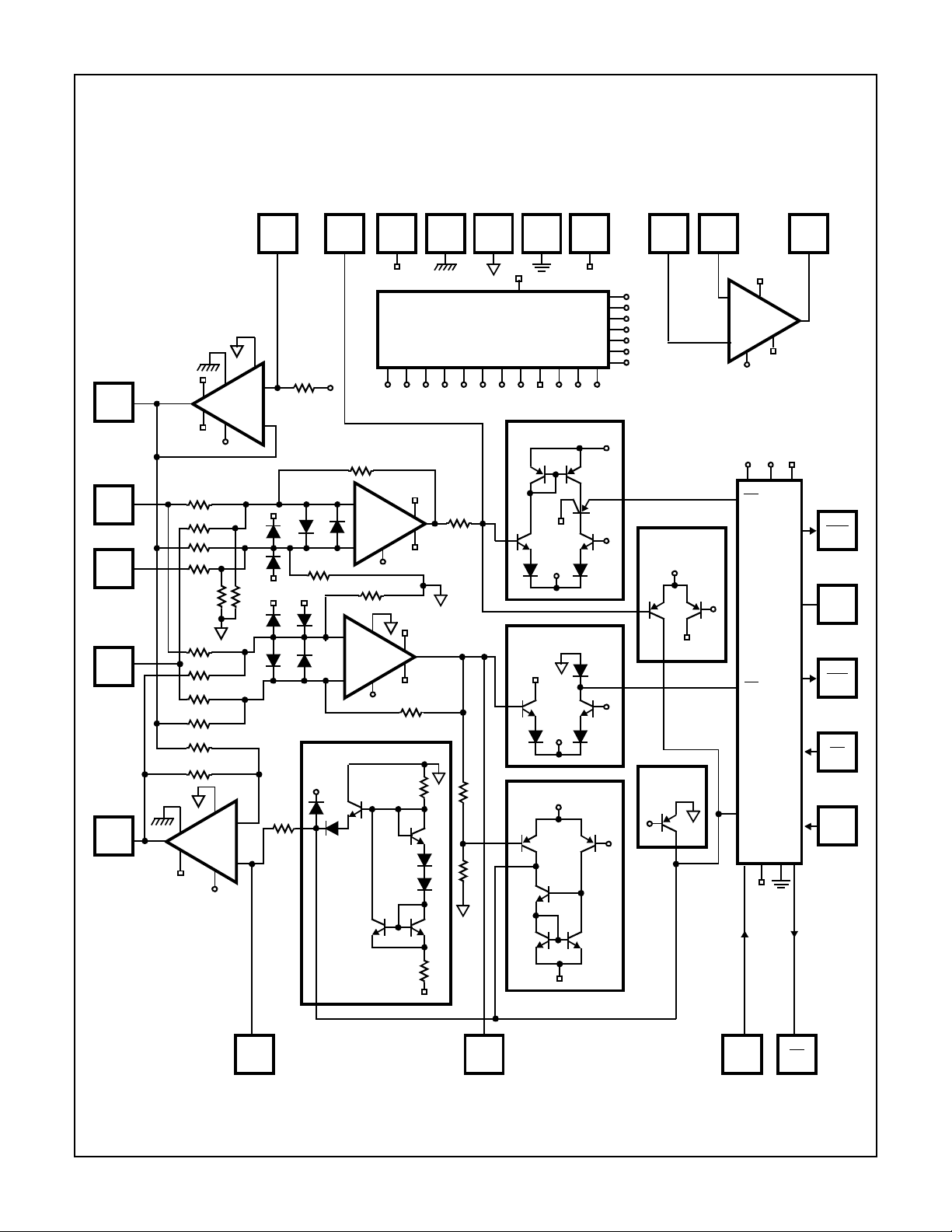
SLIC FUNCTIONAL SCHEMATIC
(DIP/SOIC PIN NUMBERS SHOWN)
TF
9
TIP
1
RING
FEED
SENSE
3
RING
2
RF
10
V
BAT
VB+
V
I
BAT
B4
R7
R8
R10
R9
R22 R23
R3
R4
R1
R2
R16
R15
A-300
RING FEED
AMP
I
B5
A-400
TIP FEED
AMP
V
-
+
21 22 11 12 23 6 4
RX C4
V
BAT ANA DIG
BAT
GND GND GND
VB+
VOLTAGE & CURRENT
BIAS NET WO RK
R17
+
V
B2
-
IB1IB2IB3IB4IB5IB6IB7I
V
B8
BAT
RING TRIP DE TE CTOR
R12
VB+
VB+
BAT
VB+
-
D36
+
A-200
LONG’L
I/V AMP
R5
I
B7
Q
Q
D3
R11
V
BAT
+
A-100
TRANSV’L
I/V AMP
I
B6
V
REFERENCE
BAT/2
V
B2
R14
R6
VB+
V
BAT
R20
V
BAT
R
18
V
+
SWITCH HO OK
DETECTOR
VB+
+
Q
D27
LOAD CURRENT
LIMITING
R21
R
19
BAT
IB9I
I
B8
I
B6
VB+
B10IB11
I
B2
20 19 18
+ - OUT
VB+
V
B1
V
B2
V
B3
V
B4
V
B5
+5V
+5V
V
B4
GND SHORTS
CURRENT
LIMITING
I
B1
-+
V
BAT
V
B1
Q
D28
THERMAL
LIMITIN G
V
B5
V
B5
-
+
V
B3
A-500
OP AMP
V
BAT
I
B3
I
B10
+5V
GK
STTL
AND LOGIC
INTERFACE
SH
RFC
V
BAT
VB+
GKD
14
C2
17
SHD
13
RC
16
PD
15
V
R13
BAT
V
BAT
TXC3 RS RD
8-24
87245
Page 7
ntinued)
HC-5504DLC
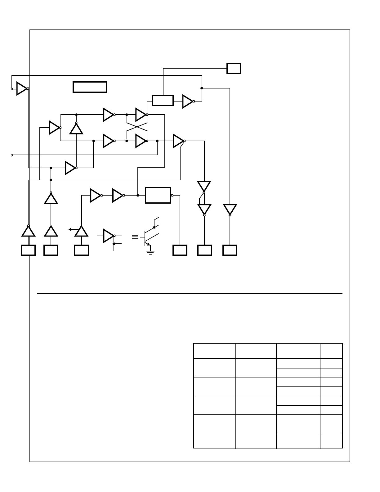
LOGIC GATE SCHEMATIC
C2
TTL
TO
STTL
TO
R21
5
10
TTL
TO
STTL
LOGIC BIAS
11 14
6
A
B
C
SCHOTTKY LOGIC
DELAY
8
97
RELAY
DRIVER
C
B
A
3
12
13
STTL
TO
TTL
STTL
TO
TTL
GKDSHDRDPDRCRS
2
4
15
TTL
TO
STTL
Die Characteristics
Transistor Count . . . . . . . . . . . . . . . . . . . . . . . . . . . . . . . 185
Diode Count . . . . . . . . . . . . . . . . . . . . . . . . . . . . . . . . . . . 36
Die Dimensions. . . . . . . . . . . . . . . . . . . . . . . . . . . 137 x 102
Substrate Potential . . . . . . . . . . . . . . . . . . . . . . . Connected
Process . . . . . . . . . . . . . . . . . . . . . . . . . . . . . . . . . Bipolar-DI
Thermal Constants (
o
C/W) θ
JA
θ
JC
Ceramic DIP . . . . . . . . . . . . . . . . . . . . 52 15
Plastic DIP. . . . . . . . . . . . . . . . . . . . . . 52 22
PLCC. . . . . . . . . . . . . . . . . . . . . . . . . . 67 29
SOIC . . . . . . . . . . . . . . . . . . . . . . . . . . 76 24
Overvoltage Protection and Longitudinal
Current Protection
The SLIC device, in conjunction with an external protection
bridge, will withstand high voltage lightning surges and
power line cross es.
High voltage surge conditions are as specified in Table 1.
The SLIC will withstand longitudinal currents up to a maxi-
mum or 30mArms, 15mArms per leg, without any performance degradation.
.
PARAMETER
Longitudinal
Surge
10µs Rise/ ±1000 (Plastic) V
1000µs/Fall ±500 (Ceram ic ) V
Metallic Surge 10µs Rise/ ±1000 (Plastic) V
1000µ Fall ±500 (Cera m ic ) V
T/GND 10µs Rise/ ±1000 (Plastic) V
R/GND 1000µs Fall ±50 0 ( Cer a m ic ) V
50/60Hz Current
T/GND 11 Cycles 700 (Plastic) V
R/GND Limited to
10Arms
TABLE 1
TEST
CONDITION
PERFORMANCE
(MAX) UNITS
350 (Ceramic) V
8-25
PEAK
PEAK
PEAK
PEAK
PEAK
PEAK
RMS
RMS
Page 8
Applications Diagram
HC-5504DLC
SUBSCRIBER
LOOP
TIP
RING
PRIMARY
PROTEC-
TION
PTC
Z
+5V TO
+12V
C
R
S1
S1
RB1
K1A
RB2
1
K1B
R
S2
C
S2
RB3
1
-48V
POWER
K1
DENIAL
8
RD
1
TIP
9
TIP FEED
VB -
10
RING FEED
3
RING FEED SENSE
RB4
2
BATT.
RING
150V PEAK (MAX)
RING GENE RATOR
SYSTEM CONTROLLER
15 13 14 7 16
SWITCH
GROUND
HOOK
DETECT
NEG.
11 12 6 23
-48V
BATT.
GND.
C8
DETECT
HC-5504DLC
KEY
SLIC
DIG.
GND.
RING
SYNC
OP AMP
ANA.
GND. V
RING
CMD
RX
+IN
-IN
OUT
C9
V
TX
C2
C3
C4
B
B
+
+
21
24
20
19
18
17
5
22
4
BALANCE NETWORK
+
C4 C3 C2
+
C6
R2
R1
C7
ZB
R3
C5
PCM
FILTER/
CODEC
SWITCHING
NETWORK
FIGURE 1. TYPICAL LINE CIRCUIT APPLICATION WITH THE MONOLITHIC SLIC
Typical Component Values
C2 = 0.15µF, 10V
C3 = 0.3µF, 30V
C4 = 0.5µF to 1.0µF, 10%, 20V (Should be nonpolarized)
C5 = 0.5µF, 20V
C6 = C7 = 0.5µF (10% Match Required) (Note 2)
C8 = 0.01µF, 100V
C9 = 0.01µF, 20V, ±20%
R1 = R2 = R3 = 100k (0.1% Match Required, 1% absolute
value) ZB = 0 for 600Ω Terminations (Note 2)
= RB2 = RB3 = RB4 = 150Ω (0.1% Match Required, 1%
RB
1
absolute value)
R
= RS2 =1kΩ, typically.
S1
= CS2 = 0.1µF, 200V typically, depending on V
C
S1
RING
and
line length.
Z
= 150V to 200V transient protection.
1
PTC used as ring generator ballast.
NOTES:
1. Second ary protection diode bridge recommended is a 2A, 200V type.
2. To obtain the specified transhybrid loss it is necessary for the three legs of the balance network, C6-R1 and R2 and C7-ZB-R3, to match
in impedance to within 0.3%. Thus, if C6 and C7 are 1µF each, a 20% match is adequate. It should be noted that the transmit output to
C6 sees a -22V step when the loop is closed. Too large a value for C6 may produce an excessively long transient at the op amp output
to the PCM Filter/CODEC.
µF and 100kΩ gives a time constant of 50msec. The uncommitted op amp output is internally clamped to stay within ±5.5V and
A 0.5
also ha s current l imiting protection .
3. All gro unds (AG, B G, & DG) mus t be applie d bef ore V
to run separate grounds off a line card, the AG must be applied first.
4. To prevent saturation of longitudinal amplifier during ringing, the ringer current should be limited to less than 30mA peak.
5. Application shows Ring inj ected ringing, a Balanced or Tip injected configuration may be used.
6. Pin numbers given for DIP/SOIC package.
Additional in formation is contained in Application Note 549, “The HC-550X Telephone SLICs’’ By Geoff Phillips
+ or VB-. Failure to do so may result in premature failure of the part. If a user wishes
B
8-26
Page 9

8-27
 Loading...