

Page 1
High Resolution Optical
Reflective Sensor
Technical Data
H
HBCS-1100
Features
• Focused Emitter and
Detector in a Single Package
• High Resolution–0.190 mm
Spot Size
• 700 nm Visible Emitter
• Lens Filtered to Reject
Ambient Light
• TO-5 Miniature Sealed
Package
• Photodiode and Transistor
Output
• Solid State Reliability
Description
The HBCS-1100 is a fully integrated module designed for
optical reflective sensing. The
module contains a 0.178 mm
(0.007 in.) diameter 700 nm
visible LED emitter and a
Package Dimensions
MAXIMUM
SIGNAL POINT
C
L
REFERENCE
5.08
(0.200)
PLANE
(0.168 ± 0.010)
4.27 ± 0.25
matched I.C. photodetector. A
bifurcated aspheric lens is used
to image the active areas of the
emitter and the detector to a
single spot 4.27 mm (0.168 in.)
in front of the package. The
reflected signal can be sensed
directly from the photodiode or
through an internal transistor
that can be configured as a high
gain amplifier.
Applications
Applications include pattern
recognition and verification,
object sizing, optical limit
switching, tachometry, textile
thread counting and defect
detection, dimensional monitoring, line locating, mark, and bar
code scanning, and paper edge
detection.
9.40 (0.370)
8.51 (0.335)
0.86 (0.034)
0.73 (0.029)
4.11
(0.162)
1.14 (0.045)
0.73 (0.029)
5.08
(0.200)
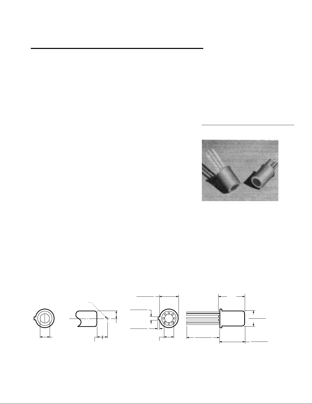
Mechanical Considerations
The HBCS-1100 is packaged in a
high profile 8 pin TO-5 metal can
with a glass window. The emitter
and photodetector chips are
mounted on the header at the
base of the package. Positioned
above these active elements is a
bifurcated aspheric acrylic lens
that focuses them to the same
point.
R.P.
8.33 (0.328)
7.79 (0.307)
11.50 (0.453)
11.22 (0.442)
15.24 (0.600)
12.70 (0.500)
S.P.
12.0
(0.473)
5965-5944E
NOTES:
1. ALL DIMENSIONS IN MILLIMETERS AND (INCHES).
2. ALL UNTOLERANCED DIMENSIONS ARE FOR REFERENCE ONLY.
3. THE REFERENCE PLANE IS THE TOP SURFACE OF THE PACKAGE.
4. NICKEL CAN AND GOLD PLATED LEADS.
5. S.P. SEATING PLANE.
6. THE LEAD DIAMETER IS 0.45 mm (0.018 IN.) TYP.
4-15
Page 2
The sensor can be rigidly secured
by commercially available two
piece TO-5 style heat sinks, such
as Thermalloy 2205, or Aavid
Engineering 3215. These fixtures
provide a stable reference platform and their tapped mounting
holes allow for ease of affixing
this assembly to the circuit board.
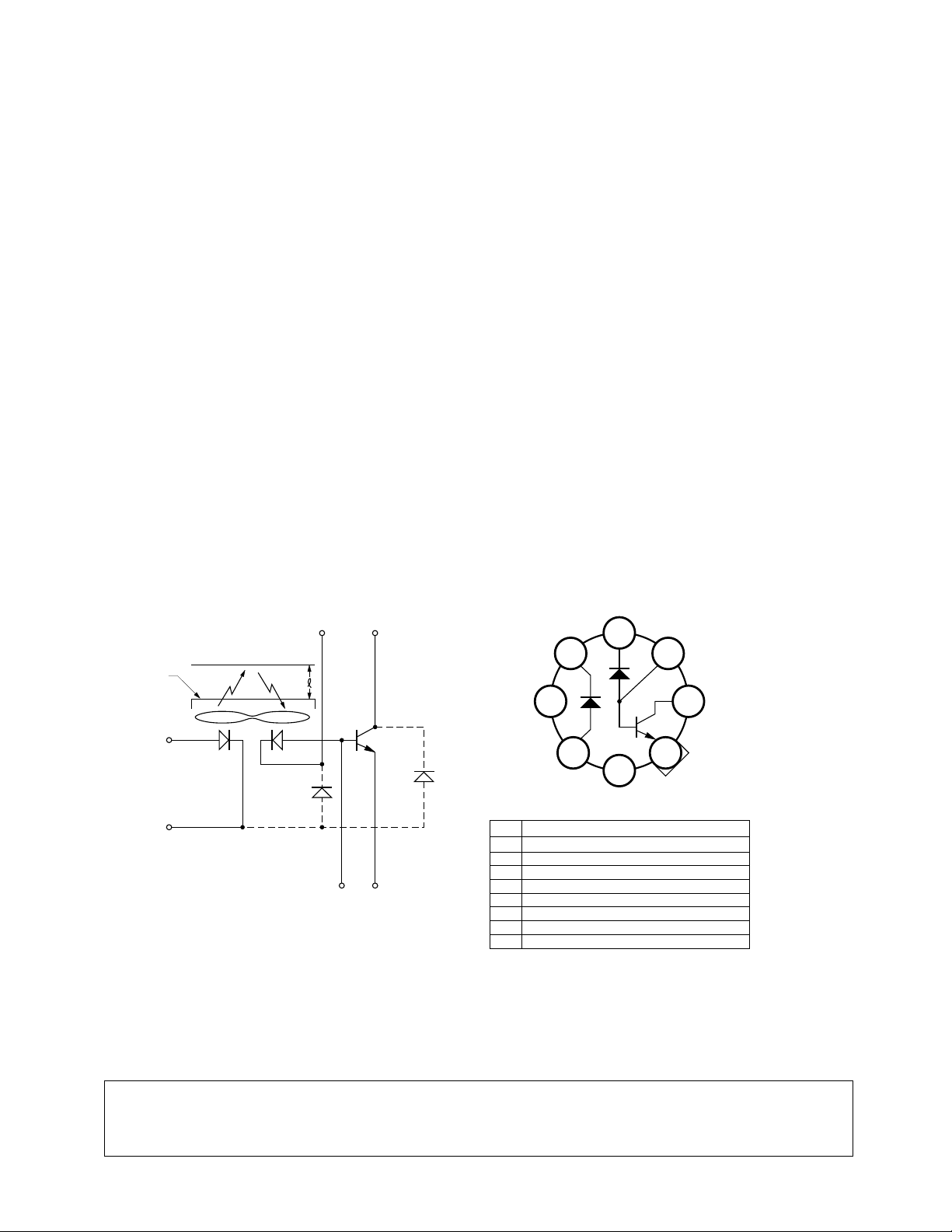
Electrical Operation
The detector section of the
sensor can be connected as a
single photodiode or as a
photodiode transistor amplifier.
When photodiode operation is
desired, it is recommended that
the substrate diodes be defeated
by connecting the collector of the
transistor to the positive potential
of the power supply and shorting
the base-emitter junction of the
transistor. Figure 15 shows
photocurrent being supplied from
the anode of the photodiode to an
inverting input of the operational
amplifier. The circuit is recommended to improve the reflected
photocurrent to stray photocurrent ratio by keeping the
substrate diodes from acting as
photodiodes.
The cathode of the 700 nm
emitter is physically and
electrically connected to the casesubstrate of the device. Applications that require modulation or
switching of the LED should be
designed to have the cathode
connected to the electrical
ground of the system. This
insures minimum capacitive
coupling of the switching
transients through the substrate
diodes to the detector amplifier
section.
The HBCS-1100 detector also
includes an NPN transistor which
can be used to increase the
output current of the sensor. A
current feedback amplifier as
shown in Figure 6 provides
moderate current gain and bias
point stability.
Schematic Diagram
REFLECTOR
REFERENCE
PLANE
ANODE
6
V
F
CATHODE
SUBSTRATE, CASE
– SUBSTRATE DIODES
D
S
4
V
D
S
V
D
31
C
28
V
V
B
E
D
S
Connection Diagram
3
42
51
68
7
PIN FUNCTION
TRANSISTOR COLLECTOR
1
TRANSISTOR BASE, PHOTODIODE ANODE
2
PHOTODIODE CATHODE
3
LED CATHODE, SUBSTRATE, CASE
4
NC
5
LED ANODE
6
NC
7
TRANSISTOR EMITTER
8
TOP VIEW
CAUTION: The small junction sizes inherent to the design of this bipolar component increase the component's
susceptibility to damage from electrostatic discharge (ESD). It is advised that normal static precautions be
taken in handling and assembly of this component to prevent damage and/or degradation which may be
introduced by ESD.
4-16
Page 3

Absolute Maximum Ratings at T
= 25°C
A
Parameter Symbol Min. Max. Units Fig. Notes
Storage Temperature T
Operating Temperature T
S
A
-40 +75 °C
-20 +70 °C
Lead Soldering Temperature 260 for 10 sec. °C11
1.6 mm from Seating Plane
Average LED Forward Current I
Peak LED Forward Current I
Reverse LED Input Voltage V
Package Power Dissipation P
Collector Output Current I
F
FPK
R
P
O
Supply and Output Voltage VD, VC, V
Transistor Base Current I
Transistor Emitter Base Voltage V
B
EB
-0.5 20 V 10
E
50 mA 2
75 mA 1 1
5V
120 mW 3
8mA
5mA
0.5 V
System Electrical/Optical Characteristics at T
= 25°C
A
Parameter Symbol Min. Typ. Max. Units Conditions Fig. Note
Total Photocurrent I
(IPR + IPS)
P
150 250 375 TA = 25°C
575 nA TA = 20°CIF = 35 mA, 2, 3 4
VD = VC = 5 V
15
80 TA = 70°C
Reflected Photocurrent I
(IPR) to Internal Stray I
PR
PS
4 8.5 IF = 35 mA, 3
VC = VD = 5 V
Photocurrent (IPS)
Transistor DC Static h
FE
Slew Rate 0.08 V/µsRL = 100 K, I
50 TA = 20° CVCE = 5 V, 4, 5
100 200 TA = 25°C
IC = 10 µACurrent Transfer Ratio
= 50 mA, 6
PK
RF = 10 M, tON = 100 µs,
Rate = 1 kHz
Image Diameter d 0.17 mm IF = 35 mA, 8, 10 8, 9
= 4.27 mm (0.168 in.)
Maximum Signal Point 4.01 4.27 4.52 mm Measured from Reference 9
Plane
50% Modulation MTF 2.5 I
npr/mmIF
= 35 mA, 10, 5, 7
Transfer Function =4.27 mm 11
Depth of Focus ∆ 1.2 mm 50% of IP at = 4.27 mm 9 5
FWHM
Effective Numerical N.A. 0.3
Aperture
Image Location D 0.51 mm Diameter Reference to 6
Centerline
= 4.27 mm
Thermal Resistance Θ
JC
85 °C/W
4-17
Page 4

Detector Electrical/Optical Characteristics at T
= 25°C
A
Parameter Symbol Min. Typ. Max. Units Conditions Fig. Note
Dark Current I
Capacitance C
PD
D
5 200 pA TA = 25°CIF = 0, VD = 5 V;
10 nA TA = 70°C
Reflection = 0%
45 pF VD = 0 V, IP = 0, f = 1 MHz
Flux Responsivity Rφ 0.22 A/W λ = 700 nm, VD = 5 V 12
Detector Area A
D
0.160 mm
2
Square, with
Length = 0.4 mm/Side
Emitter Electrical/Optical Characteristics at T
= 25°C
A
Parameter Symbol Min. Typ. Max. Units Conditions Fig. Note
Forward Voltage V
Reverse Breakdown Voltage BV
Radiant Flux φ
F
R
E
5VI
5 9.0 µWI
1.6 1.8 V IF = 35 mA 13
= 100 µA
R
= 35 mA, 14
F
λ = 700 nm
Peak Wavelength λ
Thermal Resistance Θ
Temperature Coefficient of V
F
JC
∆VF/∆T -1.2 mV/°CIF = 35 mA
Transistor Electrical Characteristics at T
680 700 720 nm IF = 35 mA 14
p
150 °C/W
= 25°C
A
Parameter Symbol Min. Typ. Max. Units Conditions Fig. Note
Collector-Emitter Leakage I
Base-Emitter Voltage V
CEO
BE
1nAV
= 5 V
CE
0.6 V IC = 10 µA, IB = 70 nA
Collector-Emitter Saturation VCE(SAT) 0.4 V IB = 1 µA, IE = 10 µA
Voltage
Collector-Base Capacitance C
Base-Emitter Capacitance C
Thermal Resistance Θ
Notes:
1. 300 µs pulse width, 1 kHz pulse rate.
2. Derate Maximum Average Current linearly from 65°C by 6 mA/°C.
3. Without heat sinking from TA = 65°C, derate Maximum Average Power linearly by 12 mW/°C.
4. Measured from a reflector coated with a 99% reflective white paint (Kodak 6080) positioned 4.27 mm (0.168 in.) from the
reference plane.
5. Peak-to-Peak response to black and white bar patterns.
6. Center of maximum signal point image lies within a circle of diameter D relative to the center line of the package. A second
emitter image (through the detector lens) is also visible. This image does not affect normal operation.
7. This measurement is made with the lens cusp parallel to the black-white transition.
8. Image size is defined as the distance for the 10%-90% response as the sensor moves over an abrupt black-white edge.
9. (+) indicates an increase in the distance from the reflector to the reference plane.
10. All voltages referenced to Pin 4.
11. CAUTION: The thermal constraints of the acrylic lens will not permit the use of conventional wave soldering procedures. The
typical preheat and post cleaning temperatures and dwell times can subject the lens to thermal stresses beyond the absolute
maximum ratings and can cause it to defocus.
CB
BE
JC
0.3 pF f = 1 MHz, VCB = 5 V
0.4 pF f = 1 MHz, VBE = 0 V
200 °C/W
4-18
Page 5

2.0
1.8
1.6
1.4
30 KHz
10 KHz
3 KHz
1 KHz
1.2
RATIO OF MAXIMUM OPERATING PEAK
CURRENT TO TEMPERATURE DERATED
MAXIMUM DC CURRENT
1.0
1 10,000
10
100 1000
tP – PULSE DURATION (µs)
F (MAX.)
I
FPK (MAX.)
I
Figure 1. Maximum Tolerable Peak Current vs. Pulse
Duration.
+5 V
300 Hz
100 Hz
1.6
= 25 °C)
PS
OR I
PR
= 35 mA, T
PHOTOCURRENT, I
(NORMALIZED AT I
-20 °C
1.4
A
1.2
1.0
0.8
F
0.6
0.4
0.2
0 °C
25 °C
50 °C
70 °C
0
080
IF – DC FORWARD CURRENT (mA)
30
10 40 6020 50 70
Figure 2. Relative Total Photocurrent
vs. LED DC Forward Current.
REFLECTOR
REFERENCE
PLANE
I
= 35 mA
F
HP 6177
NOTES:
1. I
KODAK 6080 PAINT REFLECTOR.
2. I
A CAVITY WHOSE DEPTH IS MUCH GREATER THAN
THE HBCS-1100 DEPTH OF FIELD.
+
MEASUREMENT CONDITIONS ARE: = 4.34 mm,
P
MEASUREMENT CONDITIONS ARE: =
PS
ANODE
6
V
F
CATHODE
SUBSTRATE, CASE
= I
I
P
PR
4
+ I
PS
Figure 3. IP Test Circuit.
31
D
S
28
I
P
+
NANOAMPERE METER
(KEITHLEY MODEL 480)
D
S
4-19
Page 6

3.0
= 25 °C)
A
2.0
= 100 nA, T
B
1.0
– DC FORWARD CURRENT GAIN
FE
h
0
(NORMALIZED AT I
VCE = 5 V
100
IB – BASE CURRENT (nA)
70 °C
25 °C
-20 °C
100010 10,000
50
I
– BASE CURRENT (nA)
B
TEMP = 25 °C
40
30
20
10
– COLLECTOR CURRENT (µA)
C
I
0
24 1081614 18
6
VCE – COLLECTOR-TO-EMITTER VOLTAGE (V)
160 nA
140 nA
120 nA
100 nA
80 nA
60 nA
40 nA
20 nA
12020
Figure 4. Normalized Transistor DC
Forward Current Gain vs. Base
Current at Temperature.
V
= 5 V
CC
REFLECTOR
REFERENCE
PLANE
I
= 50 mA
FPK
= 100 µs,
t
P
RATE = 1 KHz
HP 8007
ANODE
6
V
F
47 Ω
CATHODE
SUBSTRATE, CASE
4
Figure 6. Slew Rate Measurement Circuit.
Figure 5. Common Emitter Collector
Characteristics.
L
31
D
S
28
100 KR
V
O
10 MR
F
D
S
EMITTER
DETECTOR
Figure 7. Image Location.
4-20
DETECTOR IMAGE
THROUGH EMITTER
LENS
MAXIMUM
SIGNAL POINT
EMITTER IMAGE
THROUGH DETECTOR
LENS
Page 7

0.4
REFERENCE
PLANE
REFLECTOR
V
F
ANODE
6
SUBSTRATE, CASE
CATHODE
4
28
D
S
D
S
31
I
P
+
–
V
CC
V
OUT
R
2
R
1
R
F
V
CC
V
OUT
=
1 + R2/R
1
– IPR
F
0.3
0.2
0.1
d – IMAGE SIZE (mm)
0
-0.4 0.8
∆ – DISTANCE FROM MAXIMUM SIGNAL (mm)
SEE NOTES 7, 8, 9
0
-0.2 0.2 0.4 0.6
110
100
90
80
70
60
50
40
30
20
10
% – REFLECTED PHOTOCURRENT
0
06
2
1345
– REFLECTOR DISTANCE (mm)
∆
110
100
90
80
70
60
50
40
30
20
10
% – REFLECTED PHOTOCURRENT
0
-0.3 0.3
-0.2 0 0.1 0.2
∆d – EDGE DISTANCE (mm)
-0.1
90 %
10 %
d
Figure 8. Image Size vs. Maximum
Signal Point.
110
100
90
80
70
60
50
40
30
20
10
% AMPLITUDE MODULATION (P-P)
0
06
SPATIAL FREQUENCY (LINE PAIR/mm)
2
1345
Figure 11. Modulation Transfer
Function.
1.2
1.0
0.8
0.6
0.4
0.2
RELATIVE RADIANT FLUX
0
640 760
660 700 720 740
λ – WAVELENGTH (nm)
Wavelength.
0 °C
25 °C
70 °C
680
Figure 9. Reflector Distance vs.
Percent Reflected Photocurrent.
110
100
90
80
70
60
50
40
% RESPONSE
30
20
10
0
600 800 900
Figure 12. Detector Spectral
Response.
700
λ – WAVELENGTH (nm)
Figure 15. Photodiode Interconnection.Figure 14. Relative Radiant Flux vs.
25 °C
70 °C
1000
Figure 10. Step Edge Response.
100
10
1
I
F
+
0.1
– INPUT CURRENT (mA)
F
I
0.01
1.4
1.3 1.5 1.6
VF – FORWARD VOLTAGE (V)
V
F
-
Figure 13. LED Forward Current vs.
Forward Voltage Characteristics.
1.7
4-21
 Loading...