

Page 1

HB288800A5/HB288640A5
HB288448A5/HB288320A5
HB288256A5/HB288192A5
HB288160A5/HB288128A5
HB288096A5/HB288064A5
HB288032A5
FLASH ATA Card
800 MByte/640 MByte/448 MByte/320 MByte
256 MByte/192 MByte/160 MByte/128 MByte
96 MByte/64 MByte/32 MByte
ADE-203-952D (Z)
Rev. 3.0
Oct. 2, 2000
Description
HB288800A5, HB288640A5, HB288448A5, HB288320A5, HB288256A5, HB288192A5, HB288160A5,
HB288128A5, HB288096A5, HB288064A5, HB288032A5 are Flash ATA card. This card complies with PC
card ATA standard and is suitable for the usage of data storage memory medium for PC or any other electric
equipment. This card is equipped with Hitachi 256 Mega bit Flash memory. This card is suitable for ISA
(Industry Standard Architecture) bus interface standard , and read/write unit is 1 sector (512 bytes) sequential
access. By using this card it is possible to operate good performance for the system which have PC card slots.
Features
• PC card ATA standard specification
68 pin two pieces connector and Type II (5 mm)
• 3.3 V/5 V single power supply operation
• ISA standard and Read/Write unit is 512 bytes (sector) sequential access
Sector Read/Write transfer rate: 8MB/sec burst
Page 2
HB288800/640/448/320/256/192/160/128/096/064/032A5
• Card density is 800 Mega bytes maximum
This card is equipped Hitachi 256 Mega bit Flash memory
• 3 variations of mode access
Memory card mode
I/O card mode
True IDE mode
• Internal self-diagnostic program operates at VCC power on
• High reliability based on internal ECC (Error Correcting Code) function
• Data write is 300,000 cycles
• Data reliability is 1 error in 10
• Auto Sleep Function
–14
bits read.
Card Line Up*
Type No. Card density Capacity*
HB288800A5 800 MB 800,980,992 byte 1,564,416 63 16 1552
HB288640A5 640 MB 640,475,136 byte 1,250,928 63 16 1241
HB288448A5 448 MB 448,519,680 byte 876,015 63 15 927
HB288320A5 320 MB 320,409,600 byte 625,800 56 15 745
HB288256A5 256 MB 256,204,800 byte 500,400 48 15 695
HB288192A5 192 MB 192,184,320 byte 375,360 32 15 782
HB288160A5 160 MB 160,235,520 byte 312,960 32 10 978
HB288128A5 128 MB 128,188,416 byte 250,368 32 8 978
HB288096A5 96 MB 95,944,704 byte 187,392 32 8 732
HB288064A5 64 MB 64,094,208 byte 125,184 32 4 978
HB288032A5 32 MB 32,047,104 byte 62,592 32 4 489
Notes: 1. These data are written in ID.
2. Total tracks = number of head × number of cylinder.
3. Total sectors/card = sectors/track × number of head × number of cylinder.
4. It is the logical address capacity including the area which is used for file system.
1
4
Total sectors/
3
card*
Sectors/
2
track*
Number of
head
Number of
cylinder
2
Page 3
HB288800/640/448/320/256/192/160/128/096/064/032A5
Card Pin Assignment
Memory card mode I/O card mode True IDE mode
Pin No. Signal name I/O Signal name I/O Signal name I/O
1 GND — GND — GND —
2 D3 I/O D3 I/O D3 I/O
3 D4 I/O D4 I/O D4 I/O
4 D5 I/O D5 I/O D5 I/O
5 D6 I/O D6 I/O D6 I/O
6 D7 I/O D7 I/O D7 I/O
7 -CE1 I -CE1 I -CE1 I
8 A10 I A10 I A10 I
9 -OE I -OE I -ATASEL I
10——————
11 A9 I A9 I A9 I
12 A8 I A8 I A8 I
13——————
14——————
15 -WE I -WE I -WE I
16 RDY/-BSY O -IREQ O INTRQ O
17 VCC — VCC — VCC —
18——————
19——————
20——————
21——————
22 A7 I A7 I A7 I
23 A6 I A6 I A6 I
24 A5 I A5 I A5 I
25 A4 I A4 I A4 I
26 A3 I A3 I A3 I
27 A2 I A2 I A2 I
28 A1 I A1 I A1 I
29 A0 I A0 I A0 I
30 D0 I/O D0 I/O D0 I/O
31 D1 I/O D1 I/O D1 I/O
32 D2 I/O D2 I/O D2 I/O
33 WP O -IOIS16 O -IOIS16 O
3
Page 4
HB288800/640/448/320/256/192/160/128/096/064/032A5
Memory card mode I/O card mode True IDE mode
Pin No. Signal name I/O Signal name I/O Signal name I/O
34 GND — GND — GND —
35 GND — GND — GND —
36 -CD1 O -CD1 O -CD1 O
37 D11 I/O D11 I/O D11 I/O
38 D12 I/O D12 I/O D12 I/O
39 D13 I/O D13 I/O D13 I/O
40 D14 I/O D14 I/O D14 I/O
41 D15 I/O D15 I/O D15 I/O
42 -CE2 I -CE2 I -CE2 I
43 -VS1 O -VS1 O -VS1 O
44 -IORD I -IORD I -IORD I
45 -IOWR I -IOWR I -IOWR I
46——————
47——————
48——————
49——————
50——————
51 VCC — VCC — VCC —
52——————
53——————
54——————
55——————
56 -CSEL I -CSEL I -CSEL I
57 -VS2 O -VS2 O -VS2 O
58 RESET I RESET I -RESET I
59 -WAIT O -WAIT O IORDY O
60 -INPACK O -INPACK O -INPACK O
61 -REG I -REG I -REG I
62 BVD2 I/O -SPKR I/O -DASP I/O
63 BVD1 I/O -STSCHG I/O -PDIAG I/O
64 D8 I/O D8 I/O D8 I/O
65 D9 I/O D9 I/O D9 I/O
66 D10 I/O D10 I/O D10 I/O
67 -CD2 O -CD2 O -CD2 O
68 GND — GND — GND —
4
Page 5

HB288800/640/448/320/256/192/160/128/096/064/032A5
Card Pin Explanation
Signal name Direction Pin No. Description
A10 to A0
(PC Card Memory mode)
A10 to A0
(PC Card I/O mode)
A2 to A0
(True IDE mode)
BVD1
(PC Card Memory mode)
-STSCHG
(PC Card I/O mode)
-PDIAG
(True IDE mode)
BVD2
(PC Card Memory mode)
-SPKR
(PC Card I/O mode)
-DASP
(True IDE mode)
-CD1, -CD2
(PC Card Memory mode)
-CD1, -CD2
(PC Card I/O mode)
-CD1, -CD2
(True IDE mode)
-CE1, -CE2
(PC Card Memory mode)
Card Enable
-CE1, -CE2
(PC Card I/O mode)
Card Enable
-CE1, -CE2
(True IDE mode)
I 8, 11, 12, 22, 23,
24, 25, 26, 27,
28, 29
27, 28, 29 Address bus is A10 to A0. Only A2 to A0 are used,
I/O 63 BVD1 outputs the battery voltage status in the card.
I/O 62 BVD2 outputs the battery voltage status in the card.
O 36, 67 -CD1 and -CD2 are the card detection signals. -CD1
I 7, 42 -CE1 and -CE2 are low active card select signals.
Address bus is A10 to A0. A10 is MSB and A0 is
LSB.
A10 to A3 should be grounded by the host.
This output line is constantly driven to a high state
since a battery is not required for this product.
-STSCHG is used for changing the status of
Configuration and status register in attribute area.
-PDIAG is the Pass Diagnostic signal in Master/Slave
handshake protocol.
This output line is constantly driven to a high state
since a battery is not required for this product.
-SPKR outputs speaker signals. This output line is
constantly driven to a high state since this product
does not support the audio function.
-DASP is the Disk Active/Slave Present signal in the
Master/Slave handshake protocol.
and -CD2 are connected to ground in this card, so
host can detect that the card is inserted or not.
Byte/Word/Odd byte mode are defined by combination
of -CE1, -CE2 and A0.
-CE2 is used for select the Alternate Status Register
and the Device Control Register while -CE1 is the chip
select for the other task file registers.
5
Page 6

HB288800/640/448/320/256/192/160/128/096/064/032A5
Signal name Direction Pin No. Description
-CSEL
(PC Card Memory mode)
-CSEL
(PC Card I/O mode)
-CSEL
(True IDE mode)
D15 to D0
(PC Card Memory mode)
D15 to D0
(PC Card I/O mode)
D15 to D0
(True IDE mode)
GND
(PC Card Memory mode)
GND
(PC Card I/O mode)
GND
(True IDE mode)
-INPACK
(PC Card Memory mode)
-INPACK
(PC Card I/O mode)
Input Acknowledge
-INPACK
(True IDE mode)
-IORD
(PC Card Memory mode)
-IORD
(PC Card I/O mode)
-IORD
(True IDE mode)
I 56 This signal is not used.
This signal is used to configure this device as a
Master or a Slave when configured in the True IDE
mode. When this pin is grounded, this device is
configured as a Master. When the pin is open, this
device is configured as a Slave.
I/O 41, 40, 39, 38,
37, 66, 65, 64, 6,
5, 4, 3, 2, 32, 31,
30
— 1, 34, 35, 68 Ground
O 60 This signal is not used and should not be connected
I 44 This signal is not used.
Data bus is D15 to D0. D0 is the LSB of the even byte
of the word. D8 is the LSB of the odd byte of the
word.
at the host.
This signal is asserted low by this card when the card
is selected and responding to an I/O read cycle at the
address that is on the address bus during -CE and
-IORD are low. This signal is used for the input data
buffer control.
This signal is not used and should not be connected
at the host.
-IORD is used for control of read data in I/O task file
area. This card does not respond to -IORD until I/O
card interface setting up.
-IORD is used for control of read data in I/O task file
area. This card does not respond to -IORD until True
IDE interface setting up.
6
Page 7

HB288800/640/448/320/256/192/160/128/096/064/032A5
Signal name Direction Pin No. Description
-IOWR
(PC Card Memory mode)
-IOWR
(PC Card I/O mode)
-IOWR
(True IDE mode)
-OE
(PC Card Memory mode)
-OE
(PC Card I/O mode)
-ATASEL
(True IDE mode)
RDY/-BSY
(PC Card Memory mode)
-IREQ
(PC Card I/O mode)
INTRQ
(True IDE mode)
-REG
(PC Card Memory mode)
Attribute memory select
-REG
(PC Card I/O mode)
-REG
(True IDE mode)
I 45 This signal is not used.
-IOWR is used for control of data write in I/O task file
area. This card does not respond to -IOWR until I/O
card interface setting up.
-IOWR is used for control of data write in I/O task file
area. This card does not respond to -IOWR until True
IDE interface setting up.
I 9 -OE is used for the control of reading register’s data in
attribute area or task file area.
-OE is used for the control of reading register’s data in
attribute area.
To enable True IDE mode this input should be
grounded by the host.
O 16 The signal is RDY/-BSY pin. RDY/-BSY pin turns low
level during the card internal initialization operation at
VCC applied or reset applied, so next access to the
card should be after the signal turned high level.
This signal is active low -IREQ pin. The signal of low
level indicates that the card is requesting software
service to host, and high level indicates that the card
is not requesting.
This signal is the active high Interrupt Request to the
host.
I 61 -REG is used during memory cycles to distinguish
between task file and attribute memory accesses.
High for task file, Low for attribute memory is
accessed.
-REG is constantly low when task file or attribute
memory is accessed.
This input signal is not used and should be connected
to VCC.
7
Page 8
HB288800/640/448/320/256/192/160/128/096/064/032A5
Signal name Direction Pin No. Description
RESET
(PC Card Memory mode)
RESET
(PC Card I/O mode)
-RESET
(True IDE mode)
VCC
(PC Card Memory mode)
VCC
(PC Card I/O mode)
VCC
(True IDE mode)
-VS1, -VS2
(PC Card Memory mode)
-VS1, -VS2
(PC Card I/O mode)
-VS1, -VS2
(True IDE mode)
-WAIT
(PC Card Memory mode)
-WAIT
(PC Card I/O mode)
IORDY
(True IDE mode)
-WE
(PC Card Memory mode)
-WE
(PC Card I/O mode)
-WE
(True IDE mode)
I 58 This signal is active high RESET pin. If this signal is
asserted high, the card internal initialization begins to
operate. During the card internal initialization
RDY/-BSY is low. After the card internal initialization
RDY/-BSY is high.
This signal is active high RESET pin. If this signal is
asserted high, the card internal initialization begins to
operate. In this mode, RDY/-BSY signal can not be
used, so using Status Register the Ready/Busy status
can be confirmed.
This signal is active low -RESET pin. If this signal is
asserted low, all the register’s in this card are reset.
In this mode, RDY/-BSY signal can not be used, so
using status register the Ready/Busy status can be
confirmed.
— 17, 51 +5 V, +3.3 V power.
O 43, 57 These signals are intended to notify VCC requirement
to host. -VS1 is held grounded and -VS2 is
nonconnected in this card.
O 59 This signal is active low -WAIT pin. In this card this
signal is constantly high level.
This output signal may be used as IORDY. In this
card this signal is constantly high impedance.
I 15 -WE is used for the control of writing register’s data in
attribute memory area or task file area.
-WE is used for the control of writing register’s data in
attribute memory area.
This input signal is not used and should be connected
to VCC by the host.
8
Page 9

HB288800/640/448/320/256/192/160/128/096/064/032A5
Signal name Direction Pin No. Description
WP
(PC Card Memory mode)
Write Protect
-IOIS16
(PC Card I/O mode)
-IOIS16
(True IDE mode)
O 33 WP is held low because this card does not have write
protect switch.
-IOIS16 is asserted when task file registers are
accessed in 16-bit mode.
This output signal is asserted low when this device is
expecting a word data transfer cycle. Initial mode is
16-bit. If the user issues a Set Feature Command to
put the device in Byte access mode, the card permits
8-bit accesses.
9
Page 10
HB288800/640/448/320/256/192/160/128/096/064/032A5
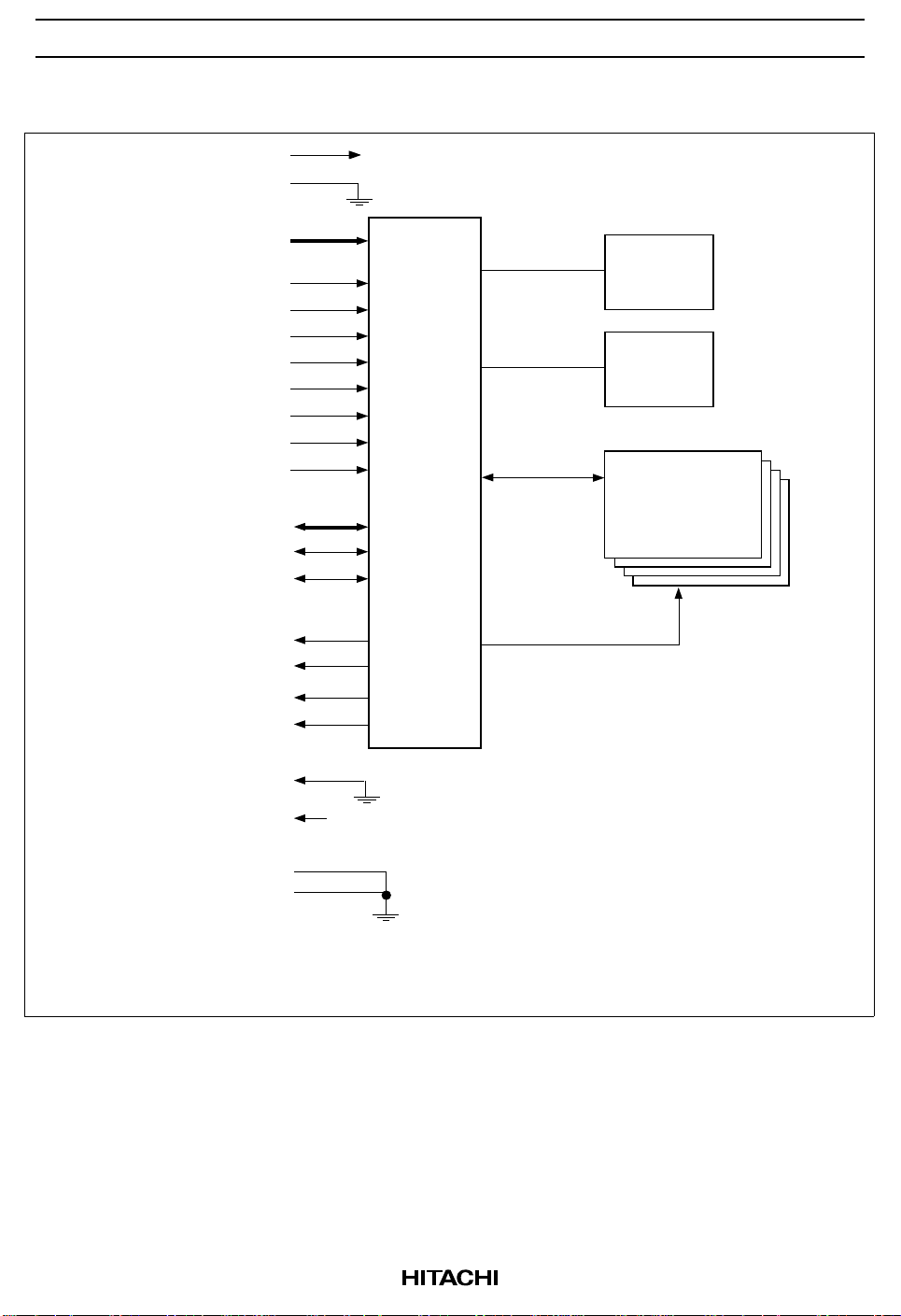
Card Block Diagram
VCC
GND
A0 to A10
-CE1,-CE2
-OE/-ATASEL
-WE
-IORD
-IOWR
-REG
RESET/-RESET
-CSEL
D0 to D15
BVD1/-STSCHG/-PDIAG
BVD2/-SPKR/-DASP
RDY/-BSY/-IREQ/INTRQ
WP/-IOIS16
internal V
Controller
CC
Reset IC
X'tal
Flash
memory
bus
Flash memory
Control signal
-INPACK
-WAIT/IORDY
-VS1
-VS2
-CD1
-CD2
Note: -CE1, -CE2, -OE, -WE, -IORD, -IOWR, -REG, RESET, -CSEL, -PDIAG, -DASP pins are
pulled up in card.
-CE1, -CE2, -OE, -WE, -IORD, -IOWR, -REG pins are schmitt trigger type input buffer.
OPEN
10
Page 11

HB288800/640/448/320/256/192/160/128/096/064/032A5
Card Function Explanation
Register construction
• Attribute region
Configuration register
• Configuration Option register
• Configuration and Status register
• Pin Replacement register
• Socket and Copy register
CIS ( C ard I nformation S tructure)
• Task File region
Data register
Error register
Feature register
Sector Count register
Sector Number register
Cylinder Low register
Cylinder High register
Drive Head register
Status register
Alternate Status register
Command register
Device Control register
Drive Address register
11
Page 12
HB288800/640/448/320/256/192/160/128/096/064/032A5
Host access specifications
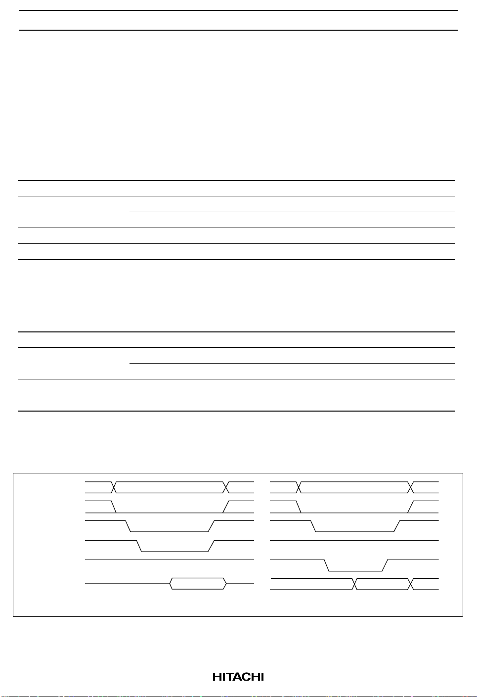
1. Attribute access specifications
When CIS-ROM region or Configuration register region is accessed, read and write operations are executed
under the condition of -REG = "L" as follows. That region can be accessed by Byte/Word/Odd-byte modes
which are defined by PC card standard specifications.
Attribute Read Access Mode
Mode -REG -CE2 -CE1 A0 -OE -WE D8 to D15 D0 to D7
Standby mode × HH×××High-Z High-Z
Byte access (8-bit) L H LLLHHigh-Z even byte
L H L H L H High-Z invalid
Word access (16-bit) L L L × L H invalid even byte
Odd byte access (8-bit) L L H × L H invalid High-Z
Note: ×: L or H
Attribute Write Access Mode
Mode -REG -CE2 -CE1 A0 -OE -WE D8 to D15 D0 to D7
Standby mode × HH×××Don’t care Don’t care
Byte access (8-bit) L H L L H L Don’t care even byte
L H L H H L Don’t care Don’t care
Word access (16-bit) L L L × H L Don’t care even byte
Odd byte access (8-bit) L L H × H L Don’t care Don’t care
Note: ×: L or H
Attribute Access Timing Example
A0 to A10
-REG
-CE2/-CE1
-OE
-WE
D0 to D15
read cycle write cycle
Dout
Din
12
Page 13
HB288800/640/448/320/256/192/160/128/096/064/032A5
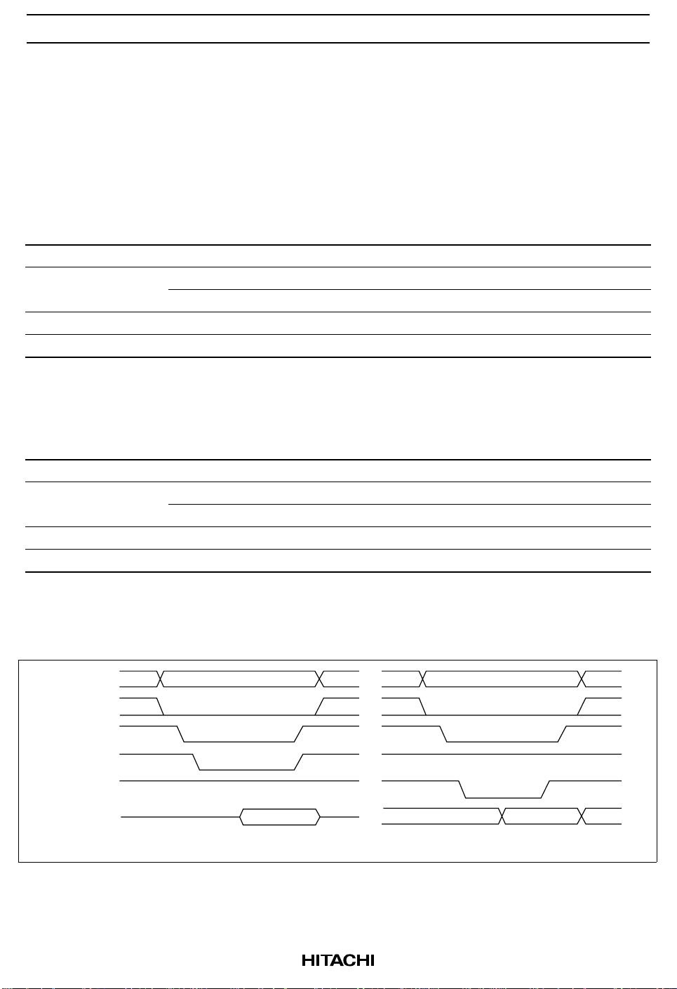
2. Task File register access specifications
There are two cases of Task File register mapping, one is mapped I/O address area, the other is mapped Memory address
area. Each case of Task File register read and write operations are executed under the condition as follows. That area can
be accessed by Byte/Word/Odd Byte mode which are defined by PC card standard specifications.
(1) I/O address map
Task File Register Read Access Mode (1)
Mode -REG -CE2 -CE1 A0 -IORD -IOWR -OE -WE D8 to D15 D0 to D7
Standby mode × HHЧЧЧЧЧHigh-Z High-Z
Byte access (8-bit) L H L L L H H H High-Z even byte
L H L H L H H H High-Z odd byte
Word access (16-bit) L L L × L H H H odd byte even byte
Odd byte access (8-bit) L L H × L H H H odd byte High-Z
Note: ×: L or H
Task File Register Write Access Mode (1)
Mode -REG -CE2 -CE1 A0 -IORD -IOWR -OE -WE D8 to D15 D0 to D7
Standby mode × HHЧЧЧЧЧDon’t care Don’t care
Byte access (8-bit) L H L L H L H H Don’t care even byte
L H L H H L H H Don’t care odd byte
Word access (16-bit) L L L × H L H H odd byte even byte
Odd byte access (8-bit) L L H × H L H H odd byte Don’t care
Note: ×: L or H
Task File Register Access Timing Example (1)
A0 to A10
-REG
-CE2/-CE1
-IORD
- IOWR
D0 to D15
Dout
read cycle write cycle
Din
13
Page 14
HB288800/640/448/320/256/192/160/128/096/064/032A5
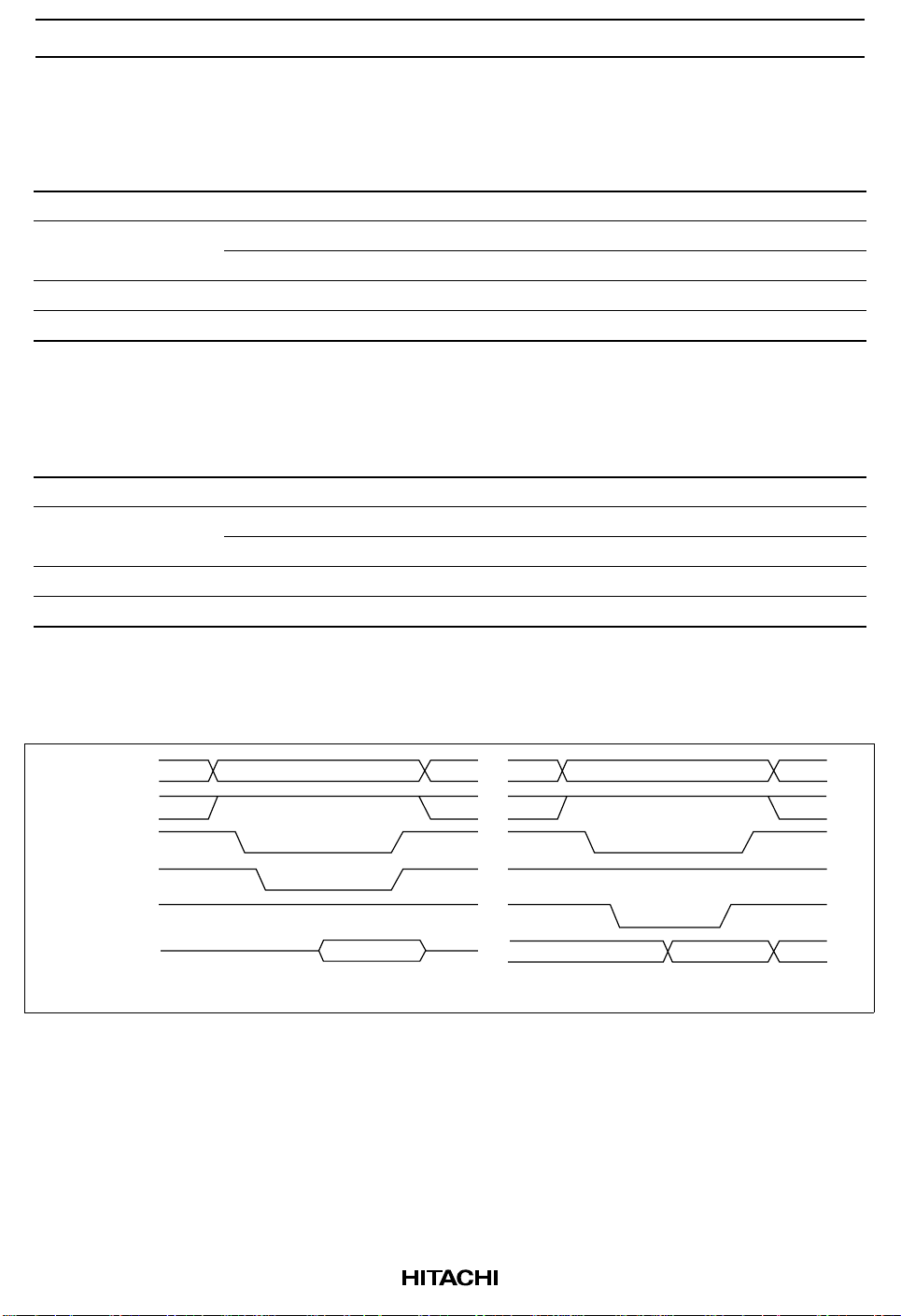
(2) Memory address map
Task File Register Read Access Mode (2)
Mode -REG -CE2 -CE1 A0 -OE -WE -IORD -IOWR D8 to D15 D0 to D7
Standby mode × HHЧЧЧЧЧHigh-Z High-Z
Byte access (8-bit) H H L L L H H H High-Z even byte
H H L H L H H H High-Z odd byte
Word access (16-bit) H L L × L H H H odd byte even byte
Odd byte access (8-bit) H L H × L H H H odd byte High-Z
Note: ×: L or H
Task File Register Write Access Mode (2)
Mode -REG -CE2 -CE1 A0 -OE -WE -IORD -IOWR D8 to D15 D0 to D7
Standby mode × HHЧЧЧЧЧDon’t care Don’t care
Byte access (8-bit) H H L L H L H H Don’t care even byte
H H L H H L H H Don’t care odd byte
Word access (16-bit) H L L × H L H H odd byte even byte
Odd byte access (8-bit) H L H × H L H H odd byte Don’t care
Note: ×: L or H
Task File Register Access Timing Example (2)
A0 to A10
-REG
-CE2/-CE1
-OE
-WE
D0 to D15
read cycle write cycle
Dout
Din
14
Page 15
HB288800/640/448/320/256/192/160/128/096/064/032A5
3. True IDE Mode
The card can be configured in a True IDE mode of operation. This card is configured in this mode only when the -OE
input signal is asserted GND by the host. In this True IDE mode Attribute Registers are not accessible from the host.
Only I/O operation to the task file and data register are allowed. If this card is configured during power on
sequence, data register are accessed in word (16-bit). The card permits 8-bit accesses if the user issues a Set
Feature Command to put the device in 8-bit mode.
True IDE Mode Read I/O Function
Mode -CE2 -CE1 A0 to A2 -IORD -IOWR D8 to D15 D0 to D7
Invalid mode L L ×××High-Z High-Z
Standby mode H H ×××High-Z High-Z
Data register access H L0LHodd byte even byte
Alternate status access L H 6H L H High-Z status out
Other task file access H L 1-7H L H High-Z data
Note: ×: L or H
True IDE Mode Write I/O Function
Mode -CE2 -CE1 A0 to A2 -IORD -IOWR D8 to D15 D0 to D7
Invalid mode L L ×××don’t care don’t care
Standby mode H H ×××don’t care don’t care
Data register access H L 0 H L odd byte even byte
Control register access L H 6H H L don’t care control in
Other task file access H L 1-7H H L don’t care data
Note: ×: L or H
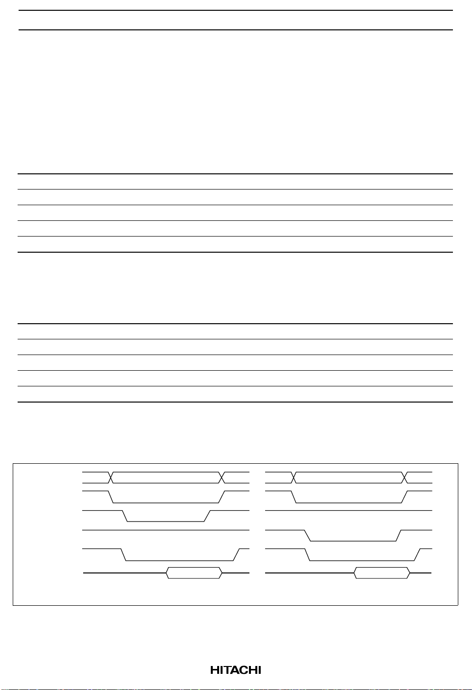
True IDE Mode I/O Access Timing Example
A0 to A2
-CE
-IORD
-IOWR
-IOIS16
D0 to D15
read cycle write cycle
Dout Din
15
Page 16

HB288800/640/448/320/256/192/160/128/096/064/032A5
Configuration register specifications
This card supports four Configuration registers for the purpose of the configuration and observation of this
card. These registers can be used in memory card mode and I/O card mode. In True IDE mode, these
registers can not be used.
1. Configuration Option register (Address 200H)
This register is used for the configuration of the card configuration status and for the issuing soft reset to the
card.
bit7 bit6 bit5 bit4 bit3 bit2 bit1 bit0
SRESET LevlREQ INDEX
Note: initial value: 00H
Name R/W Function
SRESET
(HOST->)
LevlREQ
(HOST->)
INDEX
(HOST->)
R/W Setting this bit to "1", places the card in the reset state (Card Hard Reset). This
operation is equal to Hard Reset, except this bit is not cleared. Then this bit set to "0",
places the card in the reset state of Hard Reset (This bit is set to "0" by Hard Reset) .
Card configuration status is reset and the card internal initialized operation starts when
Card Hard Reset is executed, so next access to the card should be the same sequence
as the power on sequence.
R/W This bit sets to "0" when pulse mode interrupt is selected, and "1" when level mode
interrupt is selected.
R/W This bits is used for select operation mode of the card as follows.
When Power on, Card Hard Reset and Soft Reset, this data is "000000" for the purpose
of Memory card interface recognition.
INDEX bit assignment
INDEX bit
5 4 3 2 1 0 Card mode Task File register address Mapping mode
0 0 0 0 0 0 Memory card 0H to FH, 400H to 7FFH memory mapped
0 0 0 0 0 1 I/O card xx0H to xxFH contiguous I/O mapped
0 0 0 0 1 0 I/O card 1F0H to 1F7H, 3F6H to 3F7H primary I/O mapped
0 0 0 0 1 1 I/O card 170H to 177H, 376H to 377H secondary I/O mapped
16
Page 17

HB288800/640/448/320/256/192/160/128/096/064/032A5
2. Configuration and Status register (Address 202H)
This register is used for observing the card state.
bit7 bit6 bit5 bit4 bit3 bit2 bit1 bit0
CHGED SIGCHG IOIS8 0 0 PWD INTR 0
Note: initial value: 00H
Name R/W Function
CHGED
(CARD->)
SIGCHG
(HOST->)
IOIS8
(HOST->)
PWD
(HOST->)
INTR
(CARD->)
R This bit indicates that CRDY/-BSY bit on Pin Replacement register is set to "1". When
CHGED bit is set to "1", -STSCHG pin is held "L" at the condition of SIGCHG bit set to
"1" and the card configured for the I/O interface.
R/W This bit is set or reset by the host for enabling and disabling the status-change signal (-
STSCHG pin). When the card is configured I/O card interface and this bit is set to "1", STSCHG pin is controlled by CHGED bit. If this bit is set to "0", -STSCHG pin is kept
"H".
R/W The host sets this field to "1" when it can provide I/O cycles only with on 8 bit data bus
(D7 to D0).
R/W When this bit is set to "1", the card enters sleep state (Power Down mode). When this
bit is reset to "0", the card transfers to idle state (active mode). RRDY/-BSY bit on Pin
Replacement Register becomes BUSY when this bit is changed. RRDY/-BSY will not
become Ready until the power state requested has been entered. This card
automatically powers down when it is idle, and powers back up when it receives a
command.
R This bit indicates the internal state of the interrupt request. This bit state is available
whether I/O card interface has been configured or not. This signal remains true until the
condition which caused the interrupt request has been serviced. If interrupts are
disabled by the -IEN bit in the Device Control Register, this bit is a zero.
17
Page 18

HB288800/640/448/320/256/192/160/128/096/064/032A5
3. Pin Replacement register (Address 204H)
This register is used for providing the signal state of -IREQ signal when the card configured I/O card interface.
bit7 bit6 bit5 bit4 bit3 bit2 bit1 bit0
0 0 CRDY/-BSY 0 1 1 RRDY/-BSY 0
Note: initial value: 0CH
Name R/W Function
CRDY/-BSY
(HOST->)
RRDY/-BSY
(HOST->)
4. Socket and Copy register (Address 206H)
This register is used for identification of the card from the other cards. Host can read and write this register.
This register should be set by host before this card's Configuration Option register set.
bit7 bit6 bit5 bit4 bit3 bit2 bit1 bit0
0 0 0 DRV# 0 0 0 0
Note: initial value: 00H
R/W This bit is set to "1" when the RRDY/-BSY bit changes state. This bit may also be
written by the host.
R/W When read, this bit indicates +READY pin states. When written, this bit is used for
CRDY/-BSY bit masking.
Name R/W Function
DRV#
(HOST->)
R/W This fields are used for the configuration of the plural cards. When host configures the
plural cards, written the card’s copy number in this field. In this way, host can perform
the card’s master/slave organization.
18
Page 19
HB288800/640/448/320/256/192/160/128/096/064/032A5
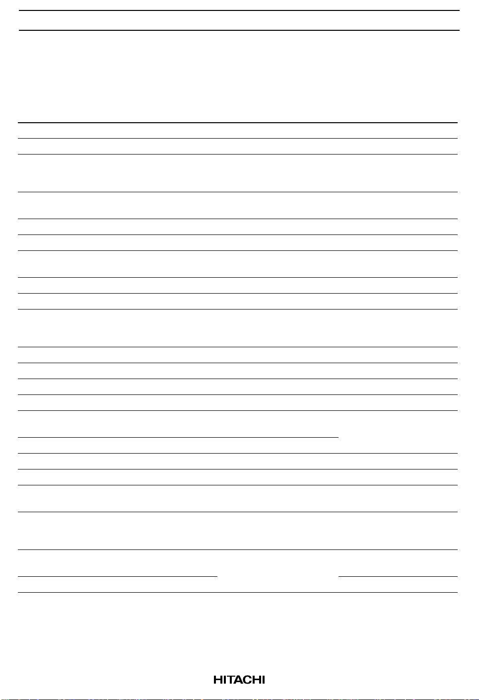
CIS informations
CIS informations are defined as follows. By reading attribute address from "0000 H", card CIS informations
can be confirmed.
Address Data 7 6 5 43210 Description of contents CIS function
000H 01H CISTPL_DEVICE Device info tuple Tuple code
002H 04H TPL_LINK Link length is 4 byte Link to next tuple
004H DFH Device type W
006H 4AH EXT Speed
mantissa
008H 01H 1x 2k units 2k byte of address space Device size
00AH FFH List end marker End of device END marker
00CH 1CH CISTPL_DEVICE_OC Other conditions device info
00EH 04H TPL_LINK Link length is 4 bytes Link to next tuple
010H 02H EXT Reserved V
012H D9H Device type W
014H 01H 1x 2k units 2k byte of address space Device size
016H FFH List end marker End of device END marker
018H 18H CISTPL_JEDEC_C JEDEC ID common memory Tuple code
01AH 02H TPL_LINK Link length is 2 bytes Link to next tuple
01CH DFH PCMCIA’s manufacturer’s JEDEC
ID code
01EH 01H PCMCIA JEDEC device code 2nd byte of JEDEC ID
020H 20H CISTPL_MANFID Manufacturer’s ID code Tuple code
022H 04H TPL_LINK Link length is 4 bytes Link to next tuple
024H 07H Low byte of PCMCIA
manufacturer’s code
026H 00H High byte of PCMCIA
manufacturer’s code
028H 00H Low byte of product code HITACHI code for PC CARD
02AH 00H High byte of product code High byte of product code
Device speed Device type = DH: I/O device
P
S
Speed
exponent
MWAIT 3 V, wait is not used Other conditions info field
CC
Device speed Device type = DH: I/O device
P
S
WPS = 1: No WP
Device speed = 7: ext speed
400 ns if no wait Extended speed
tuple
WPS = 1: No WP
Device speed = 1: 250 ns
Manufacturer’s ID code JEDEC ID of PC Card ATA
HITACHI JEDEC
manufacturer’s ID
Code of 0 because other byte
is JEDEC 1 byte
manufacture’s ID
ATA
Device type, WPS, speed
Tuple code
Device type, WPS, speed
Low byte of manufacturer’s
ID code
High byte of manufacturer’s
ID code
Low byte of product code
19
Page 20
HB288800/640/448/320/256/192/160/128/096/064/032A5
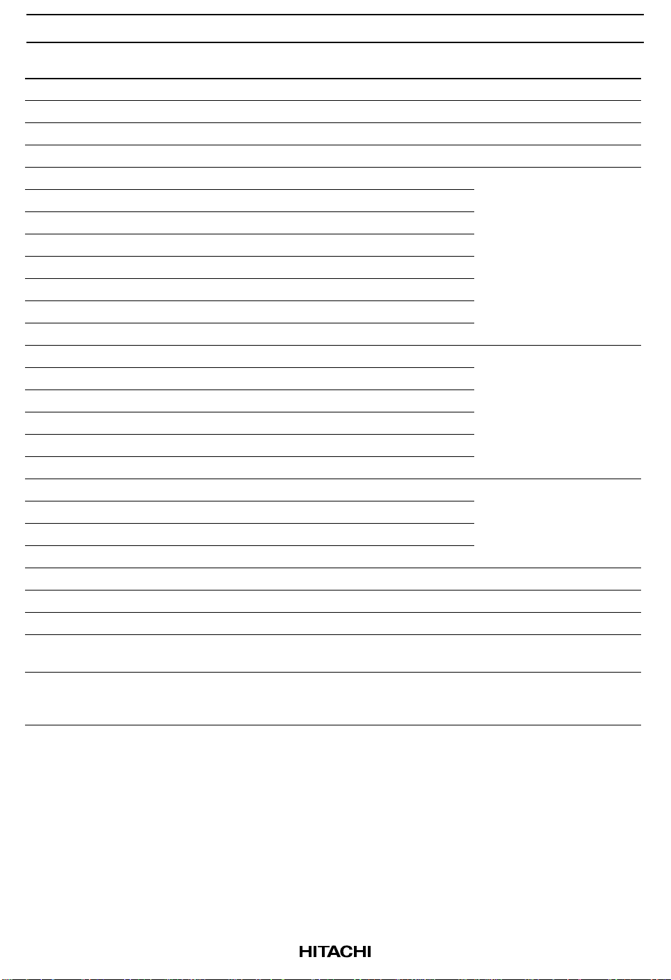
Address Data 7 6 5 43210 Description of contents CIS function
02CH 15H CISTPL_VERS_1 Level 1 version/product info Tuple code
02EH 15H TPL_LINK Link length is 15h bytes Link to next tuple
030H 04H TPPLV1_MAJOR PCMCIA2.0/JEIDA4.1 Major version
032H 01H TPPLV1_MINOR PCMCIA2.0/JEIDA4.1 Minor version
034H 48H ‘ H ’ Info string 1
036H 49H ‘ I ’
038H 54H ‘ T ’
03AH 41H ‘ A ’
03CH 43H ‘ C ’
03EH 48H ‘ H ’
040H 49H ‘ I ’
042H 00H Null terminator
044H 46H ‘ F ’ Info string 2
046H 4CH ‘ L ’
048H 41H ‘ A ’
04AH 53H ‘ S ’
04CH 48H ‘ H ’
04EH 00H Null terminator
050H 35H ‘ 5 ’ Vender specific strings
052H 2EH ‘ . ’
054H 30H ‘ 0 ’
056H 00H Null terminator
058H FFH List end marker End of device END marker
05AH 21H CISTPL_FUNCID Function ID tuple Tuple code
05CH 02H TPL_LINK Link length is 2 bytes Link to next tuple
05EH 04H TPLFID_FUNCTION = 04H Disk function, may be silicon,
may be removable
060H 01H Reserved R P R = 0: No BIOS ROM
P = 1: Configure card at
power on
PC card function code
System initialization byte
20
Page 21

HB288800/640/448/320/256/192/160/128/096/064/032A5
Address Data 7 6 5 43210 Description of contents CIS function
062H 22H CISTPL_FUNCE Function extension tuple Tuple code
064H 02H TPL_LINK Link length is 2 bytes Link to next tuple
066H 01H Disk function extension tuple type Disk interface type Extension tuple type for disk
068H 01H Disk interface type PC card ATA interface Interface type
06AH 22H CISTPL_FUNCE Function extension tuple Tuple code
06CH 03H TPL_LINK Link length is 3 bytes Link to next tuple
06EH 02H Disk function extension tuple type Single drive Extension tuple type for disk
070H 0CH Reserved D U S V No VPP, silicon, single drive
V = 0: No V
S = 1: Silicon
U = 1: Unique serial #
D = 0: Single drive on card
072H 0FH R I E N P3 P2 P1 P0 P0: Sleep mode supported
P1: Standby mode
supported
P2: Idle mode suppported
P3: Drive auto power control
N: Some config excludes
3X7
E: Index bit is emulated
I: Twin IOIS16# data reg
only
R: Reserved
074H 1AH CISTPL_CONFIG Configuration tuple Tuple code
076H 05H TPL_LINK Link length is 5 bytes Link to next tuple
078H 01H RFS RMS RAS RFS: Reserved
RMS: TPCC_RMSK si ze - 1 =
0
RAS: TPCC_RADR si ze - 1 = 1
1 byte register mask
2 byte config base address
07AH 03H TPCC_LAST Entry with config index of
03H is final entry in table
07CH 00H TPCC_RADR (LSB) Configuration registers are
located at 200H in REG
space
07EH 02H TPCC_RADR (MSB)
080H 0FH Reserved S P C I I: Configuration index
C: Configuration and status
P: Pin replacement
S: Socket and copy
required
PP
Basic ATA option
parameters byte 1
Basic ATA option
parameters byte 2
Size of fields byte TPCC_SZ
Last entry of config registers
Location of config registers
Configuration registers
present mask
TPCC_RMSK
21
Page 22

HB288800/640/448/320/256/192/160/128/096/064/032A5
Address Data 7 6 5 43210 Description of contents CIS function
082H 1BH CISTPL_CFTABLE_ENTRY Configuration table entry
tuple
084H 08H TPL_LINK Link length is 8 bytes Link to next tuple
086H C0H I D Configuration index Memory mapped I/O
configuration
I = 1: Interface byte follows
D = 1: Default entry
Configuration index = 0
088H 40H W R P B Interface type W = 0: Wait not used
R = 1: Ready active
P = 0: WP used
B = 0: BVD1 and BVD2 not
used
IF type = 0: Memory
interface
08AH A1H M MS IR IO T P M = 1: Misc info present
MS = 01: Memory space info
single 2-byte length
IR = 0: No interrupt info
present
IO = 0: No I/O port info
present
T = 0: No timing info present
P = 1: V
only info
CC
08CH 01H R DI PI AI SI HV LV NV Nominal voltage only follows
R: Reserved
DI: Power down current info
PI: Peak current info
AI: Average current info
SI: Static current info
HV: Max voltage info
LV: Min voltage info
NV: Nominal voltage info
08EH 55H X Mantissa Exponent Nominal voltage = 5 V VCC nominal value
090H 08H Length in 256 bytes pages (LSB) Length of memory space is 2kBMemory space description
092H 00H Length in 256 bytes pages (MSB)
094H 20H X R P ROA T X = 0: No more misc fields
R: Reserved
P = 1: Power down
supported
RO = 0: Not read only mode
A = 0: Audio not supported
T = 0: Single drive
Tuple code
Configuration table index
byte
TPCE_INDX
Interface description field
TPCE_IF
Feature selection byte
TPCE_FS
Power parameters for V
CC
structures (TPCE_MS)
Miscellaneous features field
TPCE_MI
22
Page 23

HB288800/640/448/320/256/192/160/128/096/064/032A5
Address Data 7 6 5 43210 Description of contents CIS function
096H 1BH CISTPL_CFTABLE_ENTRY Configuration table entry
tuple
098H 06H TPL_LINK Link length is 6 bytes Link to next tuple
09AH 00H I D Configuration index Memory mapped I/O
configuration
I = 0: No Interface byte
D = 0: No Default entry
Configuration index = 0
09CH 01H M MS IR IO T P M = 0: No Misc info
MS = 00: No Memory space
info
IR = 0: No interrupt info
present
IO = 0: No I/O port info
present
T = 0: No timing info present
P = 1: V
only info
CC
09EH 21H R DI PI AI SI HV LV NV Nominal voltage only follows
R: Reserved
DI: Power down current info
PI: Peak current info
AI: Average current info
SI: Static current info
HV: Max voltage info
LV: Min voltage info
NV: Nominal voltage info
0A0H B5H X Mantissa Exponent Nominal voltage = 3.0 V VCC nominal value
0A2H 1EH X Extension +0.3 V Extension byte
0A4H 4DH X Mantissa Exponent Max average current over 10
msec is 45 mA
Tuple code
Configuration table index
byte
TPCE_INDX
Feature selection byte
TPCE_FS
Power parameters for V
Max. average current
CC
23
Page 24

HB288800/640/448/320/256/192/160/128/096/064/032A5
Address Data 7 6 5 43210 Description of contents CIS function
0A6H 1BH CISTPL_CFTABLE_ ENTRY Configuration table entry
tuple
0A8H 0AH TPL_LINK Link length is 10 bytes Link to next tuple
0AAH C1H I D Configuration INDEX Contiguous I/O mapped ATA
registers configuration
I = 1: Interface byte follows
D = 1: Default entry
Configuration index = 1
0ACH 41H W R P B Interface type W = 0: Wait not used
R = 1: Ready active
P = 0: WP not used
B = 0: BVS1 and BVD2 not
used
IF type = 1: I/O interface
0AEH 99H M MS IR IO T P M = 1: Misc info present
MS = 00: No memory space
info
IR = 1: Interrupt info present
IO = 1: I/O port info present
T = 0: No timing info present
P = 1: V
only info
CC
0B0H 01H R DI PI AI SI HV LV NV Nominal voltage only follows
R: Reserved
DI: Power down Current info
PI: Peak current info
AI: Average current info
SI: Static current info
HV: Max voltage info
LV: Min voltage info
NV: Nominal voltage info
0B2H 55H X Mantissa Exponent Nominal voltage = 5 V VCC nominal value
0B4H 64H R S E IO AddrLine S = 1: 16-bit hosts supported
E = 1: 8-bit hosts supported
IO AddrLine: 4 lines decoded
0B6H F0H S P L M V B I N S = 1: Share logic active
P = 1: Pulse mode IRQ
supported
L = 1: Level mode IRQ
supported
M = 1: Bit mask of IRQs
present
V = 0: No vender unique IRQ
B = 0: No bus error IRQ
I = 0: No IO check IRQ
N = 0: No NMI
Tuple code
Configuration table index
byte TPCE_INDX
Interface description field
TPCE_IF
Feature selection byte
TPCE_FS
Power parameters for V
I/O space description field
TPCE_IO
Interrupt request description
structure
TPCE_IR
CC
24
Page 25

HB288800/640/448/320/256/192/160/128/096/064/032A5
Address Data 7 6 5 43210 Description of contents CIS function
0B8H FFH IRQ7IR
0BAH FFH IRQ15IR
0BCH 20H X R P RO A T X = 0: Nomore misc fields
Q
6
Q
14
IR
Q
5
IR
Q
13
IR
Q
4
IR
Q
12
IR
Q
3
IR
Q
11
IR
IR
IRQ0 IRQ level to be routed 0 to 15
Q
Q
2
1
IR
IR
IRQ8 Recommended routing to any
Q
Q
10
9
recommended
“normal, maskable” IRQ.
R: reserved
P = 1: Power down
supported
RO = 0: Not read only mode
A = 0: Audio not supported
T = 0: Single drive
Mask extension byte 1
TPCE_IR
Maskextension byte 2
TPCE_IR
Miscellaneous features field
TPCE_MI
25
Page 26

HB288800/640/448/320/256/192/160/128/096/064/032A5
Address Data 7 6 5 43210 Description of contents CIS function
0BEH 1BH CISTPL_CFTABLE_ENTRY Configuration table entry
tuple
0C0H 06H TPL_LINK Link length is 6 bytes Link to next tuple
0C2H 01H I D Configuration index Contiguous I/O mapped ATA
registers configuration
I = 0: No Interface byte
D = 0: No Default entry
Configuration index = 1
0C4H 01H M MS IR IO T P M = 0: No Misc info
MS = 00: No Memory space
info
IR = 0: No interrupt info
present
IO = 0: No I/O port info
present
T = 0: No timing info present
P = 1: V
only info
CC
0C6H 21H R DI PI AI SI HV LV NV Nominal voltage only follows
R: Reserved
DI: Power down current info
PI: Peak current info
AI: Average current info
SI: Static current info
HV: Max voltage info
LV: Min voltage info
NV: Nominal voltage info
0C8H B5H X Mantissa Exponent Nominal voltage = 3.0 V VCC nominal value
0CAH 1EH X Extension +0.3 V Extension byte
0CCH 4DH X Mantissa Exponent Max average current over 10
msec is 45 mA
Tuple code
Configuration table index
byte
TPCE_INDX
Feature selection byte
TPCE_FS
Power parameters for V
Max. average current
CC
26
Page 27

HB288800/640/448/320/256/192/160/128/096/064/032A5
Address Data 7 6 5 43210 Description of contents CIS function
0CEH 1BH CISTPL_CFTABLE_ENTRY Configuration table entry
tuple
0D0H 0FH TPL_LINK Link length is 15 bytes Link to next tuple
0D2H C2H I D Configuration INDEX ATA primary I/O mapped
configuration
I = 1: Interface byte follows
D = 1: default entry follows
Configuration index = 2
0D4H 41H W R P B Interface type W = 0: Wait not used
R = 1: Ready active
P = 0: WP not used
B = 0: BVS1 and BVD2 not
used
IF type = 1: I/O interface
0D6H 99H M MS IR IO T P M = 1: misc info present
MS = 00: No memory space
info
IR = 1: Interrupt info present
IO = 1: I/O port info present
T = 0: No timing info present
P = 1: V
only info
CC
0D8H 01H R DI PI AI SI HV LV NV Nominal voltage only follows
R: Reserved
DI: Power down Current info
PI: Peak current info
AI: Average current info
SI: Static current info
HV: Max voltage info
LV: Min voltage info
NV: Nominal voltage info
0DAH 55H X Mantissa Exponent Nominal voltage = 5 V VCC nominal value
0DCH EAH R S E IO AddrLine R = 1: Range follows
S = 1: 16-bit hosts supported
E = 1: 8-bit hosts supported
IO AddrLines: 10 lines
decoded
0DEH 61H LS AS N range LS = 1: Size of lengths is 1
byte
AS = 2: Size of address is 2
bytes
N R ang e = 1: Addr es s r ange - 1
Tuple code
Configuration table index
byte TPCE_INDX
Interface description field
TPCE_IF
Feature selection byte
TPCE_FS
Power parameters for V
I/O space description field
TPCE_IO
I/O range format description
CC
27
Page 28

HB288800/640/448/320/256/192/160/128/096/064/032A5
Address Data 7 6 5 43210 Description of contents CIS function
0E0H F0H 1st I/O base address (LSB) 1st I/O range address
0E2H 01H 1st I/O base address (MSB)
0E4H 07H 1st I/O length - 1 1st I/O range length
0E6H F6H 2nd I/O base address (LSB) 2nd I/O range address
0E8H 03H 2nd I/O base address (MSB)
0EAH 01H 2nd I/O length - 1 2nd I/O range length
0ECH EEH S P L M IRQ level S = 1: Share logic active
P = 1: Pulse mode IRQ
supported
L = 1: Level mode IRQ
supported
M = 0: Bit mask of IRQs
present
IRQ level is IRQ14
0EEH 20H X R P ROA T X = 0: Nomore misc fields
R: reserved
P = 1: Power down
supported
RO = 0: Not read only mode
A = 0: Audio not supported
T = 0: Single drive
Interrupt request description
structure
TPCE_IR
Miscellaneous features field
TPCE_MI
28
Page 29

HB288800/640/448/320/256/192/160/128/096/064/032A5
Address Data 7 6 5 43210 Description of contents CIS function
0F0H 1BH CISTPL_CFTABLE_ENTRY Configuration table entry
tuple
0F2H 06H TPL_LINK Link length is 6 bytes Link to next tuple
0F4H 02H I D Configuration index ATA primary I/O mapped
configuration
I = 0: No Interface byte
D = 0: No Default entry
Configuration index = 2
0F6H 01H M MS IR IO T P M = 0: No Misc info
MS = 00: No Memory space
info
IR = 0: No interrupt info
present
IO = 0: No I/O port info
present
T = 0: No timing info present
P = 1: V
only info
CC
0F8H 21H R DI PI AI SI HV LV NV Nominal voltage only follows
R: Reserved
DI: Power down current info
PI: Peak current info
AI: Average current info
SI: Static current info
HV: Max voltage info
LV: Min voltage info
NV: Nominal voltage info
0FAH B5H X Mantissa Exponent Nominal voltage = 3.0 V VCC nominal value
0FCH 1EH X Extension +0.3 V Extension byte
0FEH 4DH X Mantissa Exponent Max average current over 10
msec is 45 mA
Tuple code
Configuration table index
byte
TPCE_INDX
Feature selection byte
TPCE_FS
Power parameters for V
Max. average current
CC
29
Page 30

HB288800/640/448/320/256/192/160/128/096/064/032A5
Address Data 7 6 5 43210 Description of contents CIS function
100H 1BH CISTPL_CFTABLE_ENTRY Configuration table entry
tuple
102H 0FH TPL_LINK Link length is 15 bytes Link to next tuple
104H C3H I D Configuration INDEX ATA secondary I/O mapped
configuration
I = 1: Interface byte follows
D = 1: default entry
Configuration index = 3
106H 41H W R P B Interface type W = 0: Wait not used
R = 1: Ready active
P = 0: WP not used
B = 0: BVS1 and BVD2 not
used
IF type = 1: I/O interface
108H 99H M MS IR IO T P M = 1: misc info present
MS = 00: No memory space
info
IR = 1: Interrupt info present
IO = 1: I/O port info present
T = 0: No timing info present
P = 1: V
only info
CC
10AH 01H R DI PI AI SI HV LV NV Nominal voltage only follows
R: Reserved
DI: Power down Current info
PI: Peak current info
AI: Average current info
SI: Static current info
HV: Max voltage info
LV: Min voltage info
NV: Nominal voltage info
10CH 55H X Mantissa Exponent Nominal voltage = 5 V VCC nominal value
10EH EAH R S E IO AddrLine R = 1: Range follows
S = 1: 16-bit hosts supported
E = 1: 8-bit hosts supported
IO AddrLines: 10 lines
decoded
110H 61H LS AS N range LS = 1: Size of lengths is 1
byte
AS = 2: Size of address is 2
bytes
N R ang e = 1: Addr es s r ange - 1
Tuple code
Configuration table index
byte TPCE_INDX
Interface description field
TPCE_IF
Feature selection byte
TPCE_FS
Power parameters for V
I/O space description field
TPCE_IO
I/O range format description
CC
30
Page 31

HB288800/640/448/320/256/192/160/128/096/064/032A5
Address Data 7 6 5 43210 Description of contents CIS function
112H 70H 1st I/O base address (LSB) 1st I/O range address
114H 01H 1st I/O base address (MSB)
116H 07H 1st I/O length - 1 1st I/O range length
118H 76H 2nd I/O base address (LSB) 2nd I/O range address
11AH 03H 2nd I/O base address (MSB)
11CH 01H 2nd I/O length - 1 2nd I/O range length
11EH EEH S P L M IRQ level S = 1: Share logic active
P = 1: Pulse mode IRQ
supported
L = 1: Level mode IRQ
supported
M = 0: Bit mask of IRQs
present
IRQ level is IRQ14
120H 20H X R P ROA T X = 0: Nomore misc fields
R: reserved
P = 1: Power down
supported
RO = 0: Not read only mode
A = 0: Audio not supported
T = 0: Single drive
Interrupt request description
structure
TPCE_IR
Miscellaneous features field
TPCE_MI
31
Page 32
HB288800/640/448/320/256/192/160/128/096/064/032A5
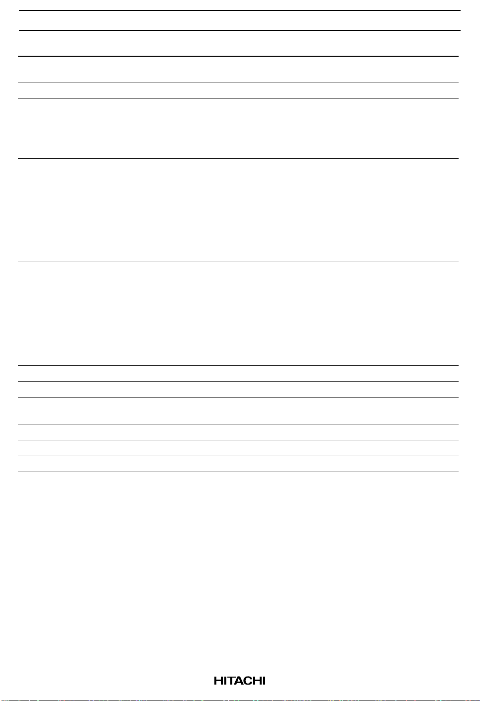
Address Data 7 6 5 43210 Description of contents CIS function
122H 1BH CISTPL_CFTABLE_ENTRY Configuration table entry
tuple
124H 06H TPL_LINK Link length is 6 bytes Link to next tuple
126H 03H I D Configuration index ATA secondary I/O mapped
configuration
I = 0: No Interface byte
D = 0: No Default entry
Configuration index = 3
128H 01H M MS IR IO T P M = 0: No Misc info
MS = 00: No Memory space
info
IR = 0: No interrupt info
present
IO = 0: No I/O port info
present
T = 0: No timing info present
P = 1: V
only info
CC
12AH 21H R DI PI AI SI HV LV NV Nominal voltage only follows
R: Reserved
DI: Power down current info
PI: Peak current info
AI: Average current info
SI: Static current info
HV: Max voltage info
LV: Min voltage info
NV: Nominal voltage info
12CH B5H X Mantissa Exponent Nominal voltage = 3.0 V VCC nominal value
12EH 1EH X Extension +0.3 V Extension byte
130H 4DH X Mantissa Exponent Max average current over 10
msec is 45 mA
132H 14H CISTPL_NO_LINK No link control tuple Tuple code
134H 00H Link is 0 bytes Link to next tuple
136H FFH CISTPL_END End of list tuple Tuple code
Tuple code
Configuration table index
byte
TPCE_INDX
Feature selection byte
TPCE_FS
Power parameters for V
Max. average current
CC
32
Page 33
HB288800/640/448/320/256/192/160/128/096/064/032A5
Task File register specification
These registers are used for reading and writing the storage data in this card. These registers are mapped five
types by the configuration of INDEX in Configuration Option register. The decoded addresses are shown as
follows.
Memory map (INDEX = 0)
-REG A10 A9 to A4 A3 A2 A1 A0 Offset -OE = L -WE = L
10× 0 0 0 0 0H Data register Data register
10× 0 0 0 1 1H Error register Feature register
10× 0 0 1 0 2H Sector count register Sector count register
10× 0 0 1 1 3H Sector number register Sector number register
10× 0 1 0 0 4H Cylinder low register Cylinder low register
10× 0 1 0 1 5H Cylinder high register Cylinder high register
10× 0 1 1 0 6H Drive head register Drive head register
10× 0 1 1 1 7H Status register Command register
10× 1 0 0 0 8H Dup. even data register Dup. even data register
10× 1 0 0 1 9H Dup. odd data register Dup. odd data register
10× 1 1 0 1 DH Dup. error register Dup. feature register
10× 1 1 1 0 EH Alt. status register Device control register
10× 1 1 1 1 FH Drive address register Reserved
11××××0 8H Even data register Even data register
11××××1 9H Odd data register Odd data register
33
Page 34
HB288800/640/448/320/256/192/160/128/096/064/032A5
Contiguous I/O map (INDEX = 1)
-REG A10 to A4 A3 A2 A1 A0 Offset -IORD = L -IOWR = L
0 × 00000H Data register Data register
0 × 00011H Error register Feature register
0 × 00102H Sector count register Sector count register
0 × 00113H Sector number register Sector number register
0 × 01004H Cylinder low register Cylinder low register
0 × 01015H Cylinder high register Cylinder high register
0 × 01106H Drive head register Drive head register
0 × 01117H Status register Command register
0 × 10008H Dup. even data register Dup. even data register
0 × 10019H Dup. odd data register Dup. odd data register
0 × 1101DHDup. error register Dup. feature register
0 × 1110EHAlt. status register Device control register
0 × 1111FH Drive address register Reserved
Primary I/O map (INDEX = 2)
-REG A10 A9 to A4 A3 A2 A1 A0 -IORD = L -IOWR = L
0 × 1FH 0000Data register Data register
0 × 1FH 0001Error register Feature register
0 × 1FH 0010Sector count register Sector count register
0 × 1FH 0011Sector number register Sector number register
0 × 1FH 0100Cylinder low register Cylinder low register
0 × 1FH 0101Cylinder high register Cylinder high register
0 × 1FH 0110Drive head register Drive head register
0 × 1FH 0111Status register Command register
0 × 3FH 0110Alt. status register Device control register
0 × 3FH 0111Drive address register Reserved
34
Page 35
HB288800/640/448/320/256/192/160/128/096/064/032A5
Secondary I/O map (INDEX = 3)
-REG A10 A9 to A4 A3 A2 A1 A0 -IORD = L -IOWR = L
0 × 17H 0000Data register Data register
0 × 17H 0001Error register Feature register
0 × 17H 0010Sector count register Sector count register
0 × 17H 0011Sector number register Sector number register
0 × 17H 0100Cylinder low register Cylinder low register
0 × 17H 0101Cylinder high register Cylinder high register
0 × 17H 0110Drive head register Drive head register
0 × 17H 0111Status register Command register
0 × 37H 0110Alt. status register Device control register
0 × 37H 0111Drive address register Reserved
True IDE Mode I/O map
-CE2 -CE1 A2 A1 A0 -IORD = L -IOWR = L
1 0 0 0 0 Data register Data register
1 0 0 0 1 Error register Feature register
1 0 0 1 0 Sector count register Sector count register
1 0 0 1 1 Sector number register Sector number register
1 0 1 0 0 Cylinder low register Cylinder low register
1 0 1 0 1 Cylinder high register Cylinder high register
1 0 1 1 0 Drive head register Drive head register
1 0 1 1 1 Status register Command register
0 1 1 1 0 Alt. status register Device control register
0 1 1 1 1 Drive address register Reserved
35
Page 36
HB288800/640/448/320/256/192/160/128/096/064/032A5
1. Data register: This register is a 16-bit register that has read/write ability, and it is used for transferring 1
sector data between the card and the host. This register can be accessed in word mode and byte mode. This
register overlaps the Error or Feature register.
bit15 bit14 bit13 bit12 bit11 bit10 bit9 bit8 bit7 bit6 bit5 bit4 bit3 bit2 bit1 bit0
D0 to D15
2. Error register: This register is a read only register, and it is used for analyzing the error content at the
card accessing. This register is valid when the BSY bit in Status register and Alternate Status register are set
to "0" (Ready).
bit7 bit6 bit5 bit4 bit3 bit2 bit1 bit0
BBK UNC “0” IDNF “0” ABRT “0” AMNF
bit Name Function
7 BBK (Bad BlocK detected) This bit is set when a Bad Block is detected in requested ID field.
6 UNC (Data ECC error) This bit is set when Uncorrectable error is occurred at reading the
card.
4 IDNF (ID Not Found) The requested sector ID is in error or cannot be found.
2 ABRT (ABoRTed command) This bit is set if the command has been aborted because of the card
status condition. (Not ready, Write fault, Invalid command, etc.)
0 AMNF (Address Mark Not Found) This bit is set in case of a general error.
3. Feature register: This register is write only register, and provides information regarding features of the
drive which the host wishes to utilize.
bit7 bit6 bit5 bit4 bit3 bit2 bit1 bit0
Feature byte
4. Sector count register: This register contains the numbers of sectors of data requested to be transferred on
a read or write operation between the host and the card. If the value of this register is zero, a count of 256
sectors is specified. In plural sector transfer, if not successfully completed, the register contains the number
of sectors which need to be transferred in order to complete the request. This register's initial value is "01H".
bit7 bit6 bit5 bit4 bit3 bit2 bit1 bit0
Sector count byte
36
Page 37

HB288800/640/448/320/256/192/160/128/096/064/032A5
5. Sector number register: This register contains the starting sector number which is started by following
sector transfer command.
bit7 bit6 bit5 bit4 bit3 bit2 bit1 bit0
Sector number byte
6. Cylinder low register: This register contains the low 8-bit of the starting cylinder address which is
started by following sector transfer command.
bit7 bit6 bit5 bit4 bit3 bit2 bit1 bit0
Cylinder low byte
7. Cylinder high register: This register contains the high 8-bit of the starting cylinder address which is
started by following sector transfer command.
bit7 bit6 bit5 bit4 bit3 bit2 bit1 bit0
Cylinder high byte
8. Drive head register: This register is used for selecting the Drive number and Head number for the
following command.
bit7 bit6 bit5 bit4 bit3 bit2 bit1 bit0
1 LBA 1 DRV Head number
bit Name Function
7 1 This bit is set to "1".
6 LBA LBA is a flag to select either Cylinder / Head / Sector (CHS) or
Logical Block Address (LBA) mode. When LBA=0, CHS mode is
selected. When LBA=1, LBA mode is selected. In LBA mode, the
Logical Block Address is interrupted as follows:
LBA07-LBA00 : Sector Number Register D7-D0.
LBA15-LBA08 : Cylinder Low Register D7-D0.
LBA23-LBA16 : Cylinder High Register D7-D0.
LBA27-LBA24 : Drive / Head Register bits HS3-HS0.
5 1 This bit is set to "1".
4 DRV (DRiVe select) This bit is used for selecting the Master (Card 0) and Slave (Card 1)
in Master/Slave organization. The card is set to be Card 0 or 1 by
using DRV# of the Socket and Copy register.
3 to 0 Head number This bit is used for selecting the Head number for the following
command. Bit 3 is MSB.
37
Page 38
HB288800/640/448/320/256/192/160/128/096/064/032A5
9. Status register: This register is read only register, and it indicates the card status of command execution.
When this register is read in configured I/O card mode (INDEX = 1, 2, 3) and level interrupt mode, -IREQ is
negated. This register should be accessed in byte mode. In word mode, it is recommended that Alternate
status register may be used as this register.
bit7 bit6 bit5 bit4 bit3 bit2 bit1 bit0
BSY DRDY DWF DSC DRQ CORR IDX ERR
bit Name Function
7 BSY (BuSY) This bit is set when the card internal operation is executing. When
this bit is set to "1", other bits in this register are invalid.
6 DRDY (Drive ReaDY) If this bit and DSC bit are set to "1", the card is capable of receiving
the read or write or seek requests. If this bit is set to "0", the card
prohibits these requests.
5 DWF (Drive Write Fault) This bit is set if this card indicates the write fault status.
4 DSC (Drive Seek Complete) This bit is set when the drive seek complete.
3 DRQ (Data ReQuest) This bit is set when the information can be transferred between the
host and Data register. This bit is cleared when the card receives
the other command.
2 CORR (CORRected data) This bit is set when a correctable data error has been occurred and
the data has been corrected.
1 IDX (InDeX) This bit is always set to "0".
0 ERR (ERRor) This bit is set when the previous command has ended in some type
of error. The error information is set in the other Status register or
Error register. This bit is cleared by the next command.
10. Alternate status register: This register is the same as Status register in physically, so the bit assignment
refers to previous item of Status register. But this register is different from Status register that -IREQ is not
negated when data read.
11. Command register: This register is write only register, and it is used for writing the command at
executing the drive operation. The command code written in the command register, after the parameter is
written in the Task File during the card is Ready state.
38
Page 39
HB288800/640/448/320/256/192/160/128/096/064/032A5
Used parameter
Command Command code FR SC SN CY DR HD LBA
Check power mode E5H or 98H N N N N Y N N
Execute drive diagnostic 90H N N N N Y N N
Erase sector C0H N Y Y Y Y Y Y
Format track 50H N Y N Y Y Y Y
Identify Drive ECH N N N N Y N N
Idle E3H or 97H N Y N N Y N N
Idle immediate E1H or 95H N N N N Y N N
Initialize drive parameters 91H N Y N N Y Y N
Read buffer E4H N N N N Y N N
Read multiple C4H N Y Y Y Y Y Y
Read long sector 22H or 23H N N Y Y Y Y Y
Read sector 20H or 21H N Y Y Y Y Y Y
Read verify sector 40H or 41H N Y Y Y Y Y Y
Recalibrate 1XH N N N N Y N N
Request sense 03H N N N N Y N N
Seek 7XH N N Y Y Y Y Y
Set features EFH Y N N N Y N N
Set multiple mode C6H N Y N N Y N N
Set sleep mode E6H or 99H N N N N Y N N
Stand by E2H or 96H N N N N Y N N
Stand by immediate E0H or 94H N N N N Y N N
Translate sector 87H N Y Y Y Y Y Y
Wear level F5H N N N N Y Y N
Write buffer E8H N N N N Y N N
Write long sector 32H or 33H N N Y Y Y Y Y
Write multiple C5H N Y Y Y Y Y Y
Write multiple w/o erase CDH N Y Y Y Y Y Y
Write sector 30H or 31H N Y Y Y Y Y Y
Write sector w/o erase 38H N Y Y Y Y Y Y
Write verify 3CH N Y Y Y Y Y Y
39
Page 40
HB288800/640/448/320/256/192/160/128/096/064/032A5
Note: FR: Feature register
SC: Sector Count register
SN: Sector Number register
CY: Cylinder register
DR: DRV bit of Drive Head register
HD: Head Number of Drive Head register
LBA: Logical Block Address Mode Supported
Y: The register contains a valid parameter for this command.
N: The register does not contain a valid parameter for this command.
12. Device control register: This register is write only register, and it is used for controlling the card
interrupt request and issuing an ATA soft reset to the card.
bit7 bit6 bit5 bit4 bit3 bit2 bit1 bit0
××××1 SRST nIEN 0
bit Name Function
7 to 4 × don't care
3 1 This bit is set to "1".
2 SRST (Software ReSeT) This bit is set to "1" in order to force the card to perform Task File
Reset operation. This does not change the Card Configuration
registers as a Hardware Reset does. The card remains in Reset
until this bit is reset to "0".
1 nIEN (Interrupt ENable) This bit is used for enabling -IREQ. When this bit is set to "0", -IREQ
is enabled. When this bit is set to "1", -IREQ is disabled.
0 0 This bit is set to "0".
13. Drive Address register: This register is read only register, and it is used for confirming the drive status.
This register is provides for compatibility with the AT disk drive interface. It is recommended that this
register is not mapped into the host’s I/O space because of potential conflicts on bit7.
bit7 bit6 bit5 bit4 bit3 bit2 bit1 bit0
× nWTG nHS3 nHS2 nHS1 nHS0 nDS1 nDS0
bit Name Function
7 × This bit is unknown
6 nWTG (WriTing Gate) This bit is unknown
5 to 2 nHS3-0 (Head Select3-0) These bits is the negative value of Head Select bits (bit 3 to 0) in
Drive/Head register.
1 nDS1 (Idrive Select1) This bit is unknown
0 nDS0 (Idrive Select0) This bit is unknown
40
Page 41
HB288800/640/448/320/256/192/160/128/096/064/032A5
ATA Command specifications
This table summarizes the ATA command set with the paragraphs. Following shows the support commands
and command codes which are written in command registers.
ATA Command Set
No. Command set Code FR SC SN CY DR HD LBA
1 Check power mode E5H or 98H — — — — Y — —
2 Execute drive diagnostic 90H — — — — Y — —
3 Erase sector(s) C0H — Y Y Y Y Y Y
4 Format track 50H — Y — Y Y Y Y
5 Identify Drive ECH — — — — Y — —
6 Idle E3H or 97H — Y — — Y — —
7 Idle immediate E1H or 95H — — — — Y — —
8 Initialize drive parameters 91H — Y — — Y Y —
9 Read buffer E4H — — — — Y — —
10 Read multiple C4H — Y Y Y Y Y Y
11 Read long sector 22H, 23H — — Y Y Y Y Y
12 Read sector (s) 20H, 21H — Y Y Y Y Y Y
13 Read verify sector (s) 40H, 41H — Y Y Y Y Y Y
14 Recalibrate 1XH — — — — Y — —
15 Request sense 03H — — — — Y — —
16 Seek 7XH — — Y Y Y Y Y
17 Set features EFH Y — — — Y — —
18 Set multiple mode C6H — Y — — Y — —
19 Set sleep mode E6H or 99H — — — — Y — —
20 Stand by E2H or 96H — — — — Y — —
21 Stand by immediate E0H or 94H — — — — Y — —
22 Translate sector 87H — Y Y Y Y Y Y
23 Wear level F5H — — — — Y Y —
24 Write buffer E8H — — — — Y — —
25 Write long sector 32H or 33H — — Y Y Y Y Y
26 Write multiple C5H — Y Y Y Y Y Y
27 Write multiple w/o erase CDH — Y Y Y Y Y Y
28 Write sector 30H or 31H — Y Y Y Y Y Y
29 Write sector(s) w/o erase 38H — Y Y Y Y Y Y
30 Write verify 3CH — Y Y Y Y Y Y
41
Page 42

HB288800/640/448/320/256/192/160/128/096/064/032A5
Note: FR: Feature Register
SC: Sector Count register (00H to FFH)
SN: Sector Number register (01H to 20H)
CY: Cylinder Low/High register (to)
DR: Drive bit of Drive/Head register
HD: Head No.(0 to 3) of Drive/Head register
NH: No. of Heads
Y: Set up
—: Not set up
1. Check Power Mode (code: E5H or 98H): This command checks the power mode.
2. Execute Drive Diagnostic (code: 90H): This command performs the internal diagnostic tests implemented
by the Card.
3. Erase Sector(s) (code: C0H): This command is used to erase data sectors.
4. Format Track (code: 50H): This command writes the desired head and cylinder of the selected drive.
But selected sector data is not exchange. This card excepts a sector buffer of data from the host to follow the
command with same protocol as the Write Sector Command.
5. Identify Drive (code: ECH): This command enables the host to receive parameter information from the
Card.
42
Page 43
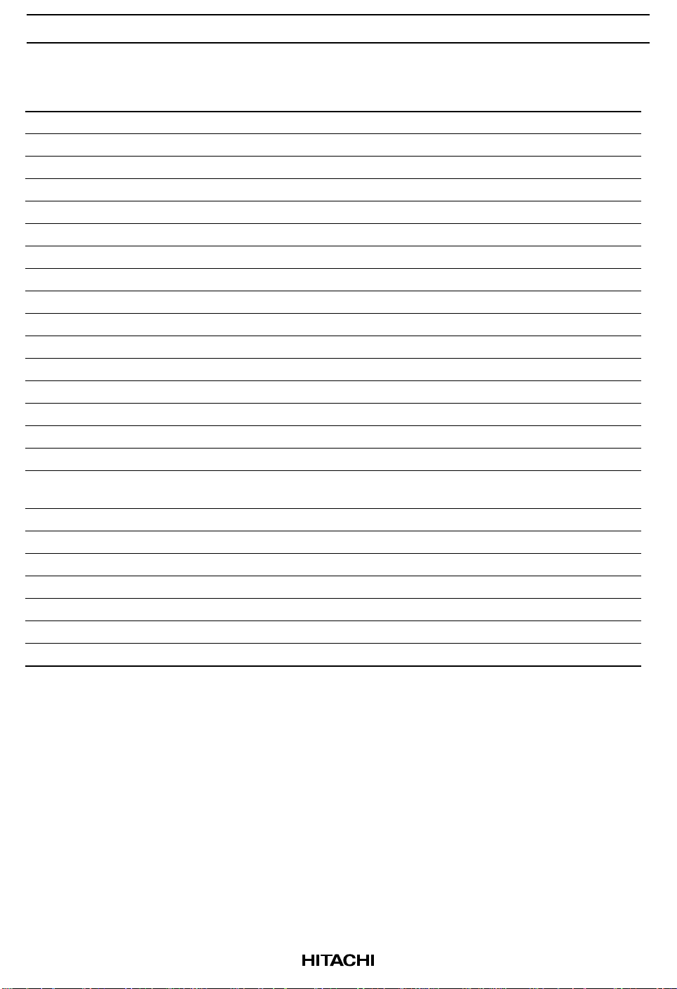
HB288800/640/448/320/256/192/160/128/096/064/032A5
Identify Drive Information
Word address Default value Total bytes Data field type information
0 848AH 2 General configuration bit-significant information
1 XXXX 2 Default number of cylinders
2 0000H 2 Reserved
3 00XXH 2 Default number of heads
4 0000H 2 Number of unformatted bytes per track
5 XXXX 2 Number of unformatted bytes per sector
6 XXXX 2 Default number of sectors per track
7 to 8 XXXX 4 Number of sectors per card (Word7 = MSW, Word8 = LSW)
9 0000H 2 Reserved
10 to 19 XXXX 20 Reserved
20 0002H 2 Buffer type (dual ported)
21 0002H 2 Buffer size in 512 byte increments
22 0004H 2 # of ECC bytes passed on Read/Write Long Commands
23 to 46 XXXX 48 Firmware revision in ASCII etc.
47 0001H 2 Maximum of 1 sector on Read/Write Multiple command
48 0000H 2 Double Word not supported
49 0200H 2 Capabilities: DMA NOT Supported (bit 8), LBA supported
(bit9)
50 0000H 2 Reserved
51 0100H 2 PIO data transfer cycle timing mode 1
52 0000H 2 DMA data transfer cycle timing mode not Supported
53 to 58 XXXX 12 Reserved
59 010XH 2 Multiple sector setting is valid
60 to 61 XXXX 4 Total number of sectors addressable in LBA Mode
62 to 255 0000H 388 Reserved
6. Idle (code: E3H or 97H): This command causes the Card to set BSY, enter the Idle mode, clear BSY and
generate an interrupt. If sector count is non-zero, the automatic power down mode is enabled. If the sector
count is zero, the automatic power down mode is disabled.
7. Idle Immediate (code: E1H or 95H): This command causes the Card to set BSY, enter the Idle (Read)
mode, clear BSY and generate an interrupt.
8. Initialize Drive Parameters (code: 91H): This command enables the host to set the number of sectors per
track and the number of heads per cylinder.
9. Read Buffer (code: E4H): This command enables the host to read the current contents of the card's sector
buffer.
43
Page 44

HB288800/640/448/320/256/192/160/128/096/064/032A5
10. Read Multiple (code: C4H): This command performs similarly to the Read Sectors command.
Interrupts are not generated on each sector, but on the transfer of a block which contains the number of
sectors defined by a Set Multiple command.
11. Read Long Sector (code: 22H or 23H): This command performs similarly to the Read Sector(s)
command except that it returns 516 bytes of data instead of 512 bytes.
12. Read Sector(s) (code: 20H, 21H): This command reads from 1 to 256 sectors as specified in the Sector
Count register. A sector count of 0 requests 256 sectors. The transfer begins at the sector specified in the
Sector Number register.
13. Read Verify Sector(s) (code: 40H or 41H): This command is identical to the Read Sectors command,
except that DRQ is never set and no data is transferred to the host .
14. Recalibrate (code: 1XH): This command is effectively a NOP command to the Card and is provided for
compatibility purposes.
15. Request Sense (code: 03H): This command requests an extended error code after command ends with an
error.
16. Seek (code: 7XH): This command is effectively a NOP command to the Card although it does perform a
range check.
17. Set Features (code: EFH): This command is used by the host to establish or select certain features.
Feature Operation
01H Enable 8-bit data transfers.
55H Disable Read Look Ahead.
66H Disable Power on Reset (POR) establishment of defaults at Soft Reset.
81H Disable 8-bit data transfers.
BBH 4 bytes of data apply on Read/Write Long commands.
CCH Enable Power on Reset (POR) establishment of defaults at Soft Reset.
18. Set Multiple Mode (code: C6H): This command enables the Card to perform Read and Write Multiple
operations and establishes the block count for these commands.
19. Set Sleep Mode (code: E6H or 99H): This command causes the Card to set BSY, enter the Sleep mode,
clear BSY and generate an interrupt.
20. Stand By (code: E2H or 96H): This command causes the Card to set BSY, enter the Sleep mode (which
corresponds to the ATA "Standby" Mode), clear BSY and return the interrupt immediately.
21. Stand By Immediate (code: E0H or 94H): This command causes the Card to set BSY, enter the Sleep
mode(which corresponds to the ATA "Standby" Mode), clear BSY and return the interrupt immediately.
44
Page 45

HB288800/640/448/320/256/192/160/128/096/064/032A5
22. Translate Sector (code: 87H): This card does not support by this command the function of determining
the exact number of times a user sector has been erased and programmed because this card always responds
with “00H”, though this command could provide information containing the desired cylinder, head and sector,
including its Logical Address, etc.
23. Wear Level (code: F5H): This command effectively a NOP command and only implemented for
backward compatibility. The Sector Count Register will always be returned with an 00H indicating Wear
Level is not needed.
24. Write Buffer (code: E8 H): This command enables the host to overwrite contents of the Card's sector
buffer with any data pattern desired.
25. Write Long Sector (code: 32H or 33H): This command is provided for compatibility purposes and is
similar to the Write Sector(s) command except that it writes 516 bytes instead of 512 bytes.
26. Write Multiple (code: C5H): This command is similar to the Write Sectors command. Interrupts are not
presented on each sector, but on the transfer of a block which contains the number of sectors defined by Set
Multiple command.
27. Write Multiple without Erase (code: CDH): This command is similar to the Write Multiple command
with the exception that an implied erase before write operation is not performed.
28. Write Sector(s) (code: 30H or 31H): This command writes from 1 to 256 sectors as specified in the
Sector Count register. A sector count of zero requests 256 sectors. The transfer begins at the sector specified
in the Sector Number register.
29. Write Sector(s) without Erase (code: 38H): This command is similar to the Write Sector(s) command
with the exception that an implied erase before write operation is not performed.
30. Write Verify (code: 3CH): This command is similar to the Write Sector(s) command, except each sector
is verified immediately after being written.
45
Page 46
HB288800/640/448/320/256/192/160/128/096/064/032A5
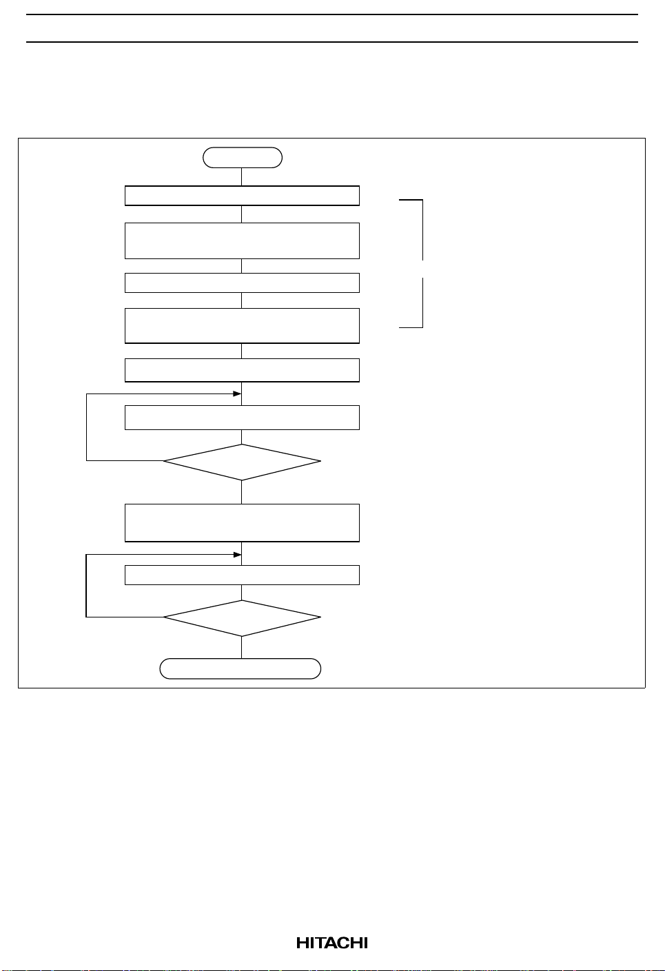
Sector Transfer Protocol
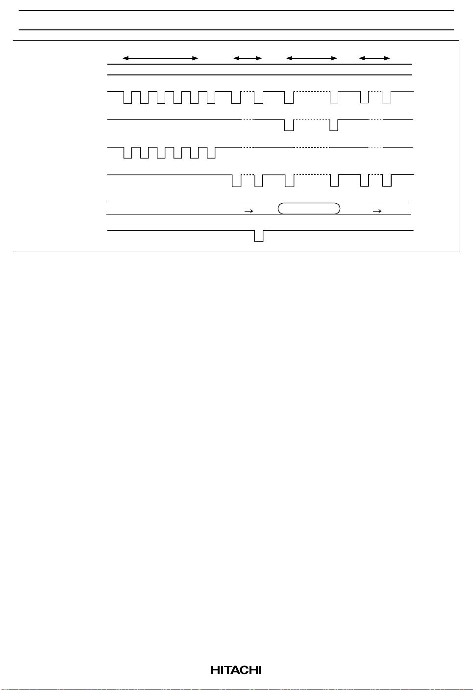
1. Sector read: 1 sector read procedure after the card configured I/O interface is shown as follows.
Start
Set the cylinder low / high register
Set the head No. of drive head register
Set the sector number register
Set "01H" in sector count register
Set "20H" in Command register
Read the status register
N
Read 256 times the data register
"58H"?
Y
(512 bytes)
I/O Access, INDEX=1
(1)Set the logical sector number
(2)
(3)
(4)Burst data transfer
46
Read the status register
N
Wait the command input
"50H"?
(5)
Y
Page 47
HB288800/640/448/320/256/192/160/128/096/064/032A5
(1) (2) (3) (4) (5)
A0 to A10
-CE1
-CE2
-IOWR
-IORD
D0 to D15
-IREQ
4H 5H 6H 3H 2H 7H 7H 7H 0H 0H 7H 7H
01H20H 80H 58H 50H80H
Data transfer
47
Page 48
HB288800/640/448/320/256/192/160/128/096/064/032A5
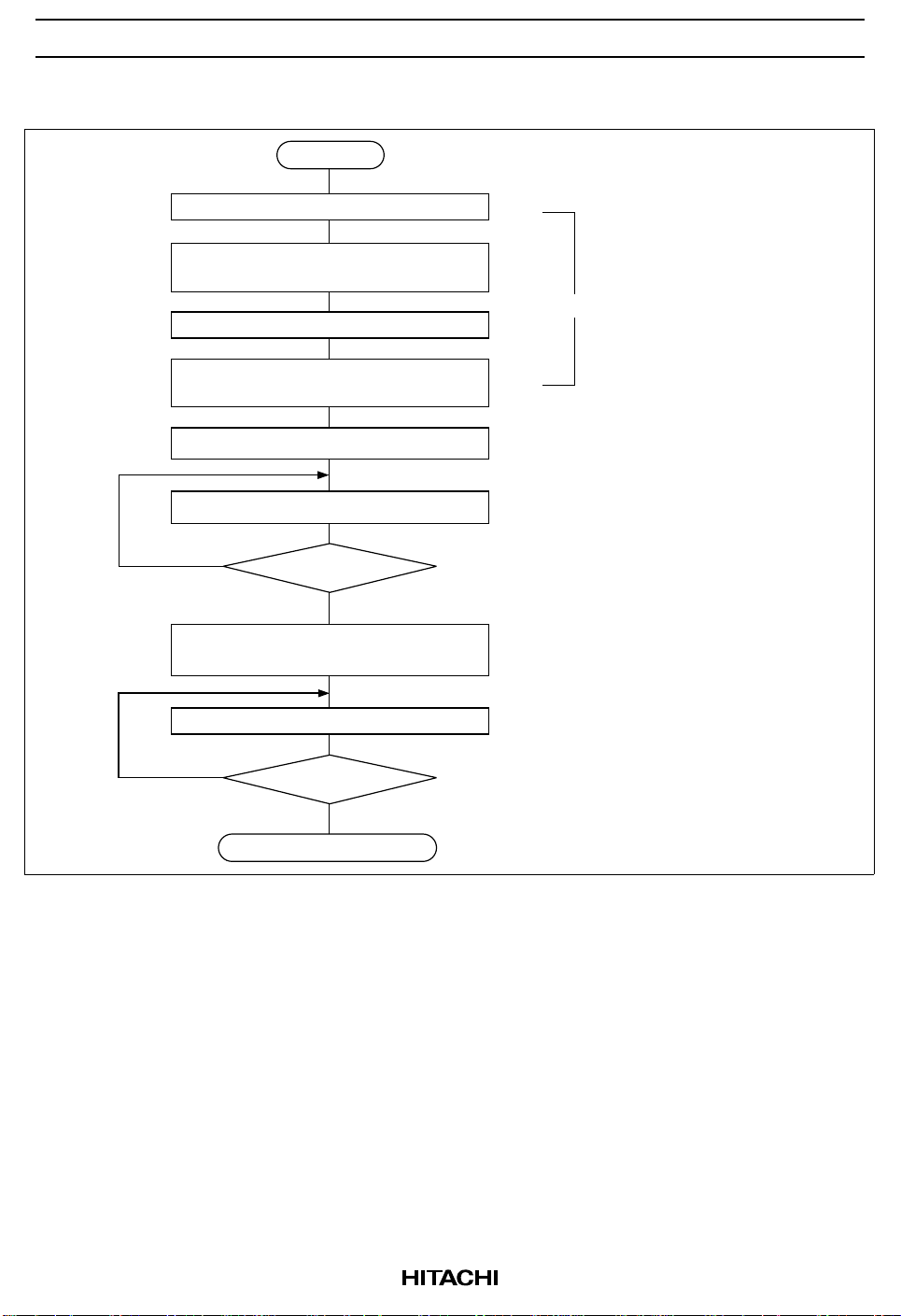
2. Sector write: 1 sector write procedure after the card configured I/O interface is shown as follows.
Start
Set the cylinder low / high register
Set the head No. of drive head register
Set the sector number register
Set "01H" in sector count register
Set "30H" in command register
Read the status register
N
Write 256 times the data register
"58H"?
Y
(512 bytes)
I/O Access, INDEX=1
(1) Set the logical sector number
(2)
(3)
(4) Burst data transfer
Read the status register
N
Wait the command input
"50H"?
(5)
Y
48
Page 49
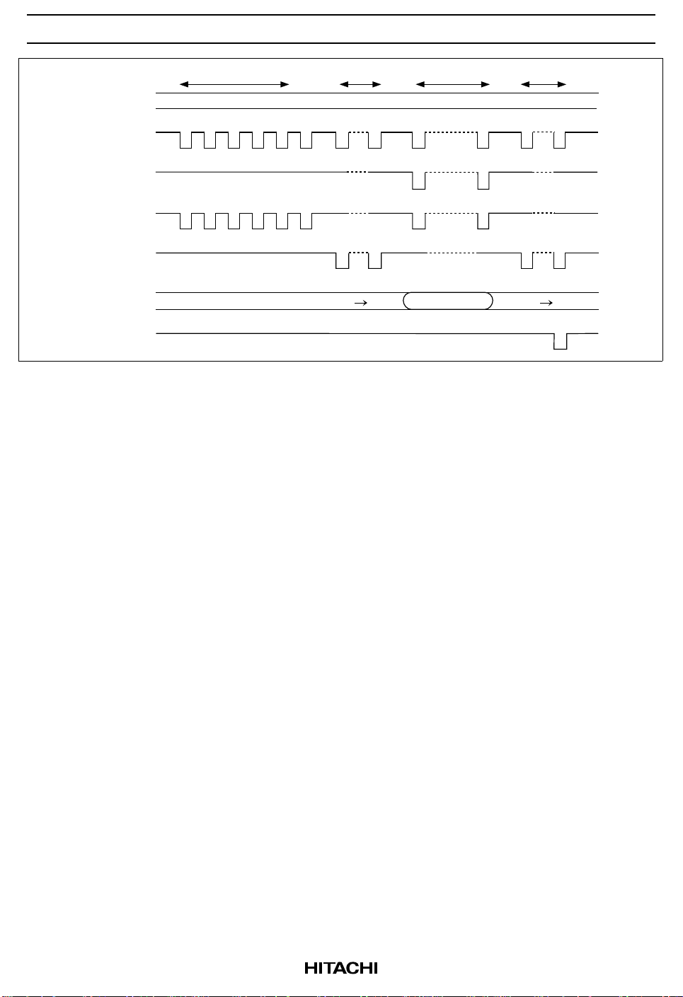
HB288800/640/448/320/256/192/160/128/096/064/032A5
(1) (2) (3) (4) (5)
A0 to A10
-CE1
-CE2
-IOWR
-IORD
D0 to D15
-IREQ
4H 5H 6H 3H 2H 7H 7H 7H 0H 0H 7H 7H
01H30H 80H 58H 50H80H
Data transfer
49
Page 50
HB288800/640/448/320/256/192/160/128/096/064/032A5
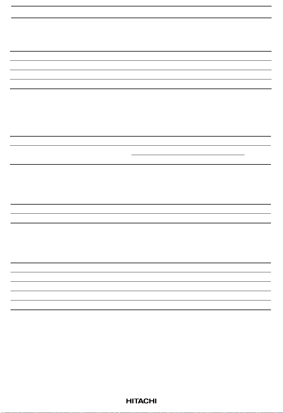
Absolute Maximum Ratings
Parameter Symbol Value Unit Note
All input/output voltages Vin, Vout –0.3 to V
VCC voltage V
Operating temperature range Topr 0 to +60 °C
Storage temperature range Tstg –20 to +65 °C
Note: 1. Vin, Vout min = –2.0 V for pulse width ≤ 20 ns.
CC
–0.3 to +6.5 V
Recommended DC Operating Conditions
Parameter Symbol Min Typ Max Unit Note
Operating temperature Ta 0 25 60 ˚C
VCC voltage V
CC
4.5 5.0 5.5 V
3.15 3.3 3.45 V
+ 0.3 V 1
CC
Capacitance (Ta = 25˚C, f = 1MHz)
Parameter Symbol Min Typ Max Unit Test conditions
Input capacitance Cin — — 35 pF Vin = 0 V
Output capacitance Cout — — 35 pF Vout = 0 V
System Performance
Item Performance
Start up times (Reset to ready) 100 ms (max)
Start up times (Sleep to idle) 2 ms (max)
Data transfer rate to/from host 8 MB/s burst
Controller overhead (Command to DRQ) 2 ms (max)
Data transfer cycle end to ready (Sector write) 2 ms (typ)
50
Page 51
HB288800/640/448/320/256/192/160/128/096/064/032A5
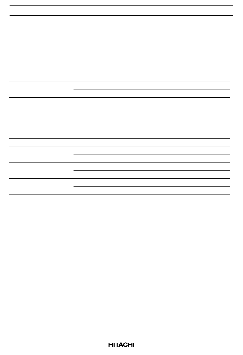
DC Characteristics-1 (Ta = 0 to +60˚C, VCC = 5.0 V ± 10%)
Parameter Symbol Min Typ Max Unit Test conditions Note
Input leakage current I
Input voltage (CMOS) V
Input voltage (schmitt trigger) V
Output voltage V
LI
IL
V
IH
IL
V
IH
OL
V
OH
——± 1 µA Vin = GND to V
— — 0.8 V
4.0 — — V
— 2.0 — V
— 2.8 — V
— — 0.4 V IOL = 8 mA
VCC – 0.8 — — V IOH = –8 mA
Note: 1. Except pulled up input pin.
DC Characteristics-2 (Ta = 0 to +60˚C, VCC = 3.3 V ± 5%)
Parameter Symbol Min Typ Max Unit Test conditions Note
Input leakage current I
Input voltage (CMOS) V
Input voltage (schmitt trigger) V
Output voltage V
LI
IL
V
IH
IL
V
IH
OL
V
OH
Note: 1. Except pulled up input pin.
——± 1 µA Vin = GND to V
— — 0.6 V
2.4 — — V
— 1.0 — V
— 1.8 — V
— — 0.4 V IOL = 8 mA
VCC – 0.8 — — V IOH = –8 mA
1
CC
1
CC
51
Page 52

HB288800/640/448/320/256/192/160/128/096/064/032A5
DC Characteristics-3 (Ta = 0 to +60˚C, VCC = 5.0 V ± 10%)
32MB/64MB/
96MB/
128MB
160MB/192
MB/256MB/
320MB
448MB/640
MB/800MB
Parameter Symbol Typ Max Typ Max Typ Max Unit Test conditions
Sleep/standby
current
I
SP1
0.5 1.0 0.7 1.5 1.0 2.0 mA CMOS level (control signal =
V
– 0.2 V)
CC
(In Memory card mode and
I/O card mode)
Sector read
current
I
(DC) 40 75 40 75 40 75 mA CMOS level (control signal =
CCR
V
– 0.2 V) during sector
CC
read transfer
I
CCR
80 120 80 120 80 120 mA
(Peak)
Sector write
current
I
(DC) 45 75 45 75 45 75 mA CMOS level (control signal =
CCW
V
– 0.2 V) during sector
CC
write transfer
I
CCW
80 120 80 120 80 120 mA
(Peak)
DC Characteristics-4 (Ta = 0 to +60˚C, VCC = 3.3 V ± 5%)
32MB/64MB/
96MB/
128MB
Parameter Symbol Typ Max Typ Max Typ Max Unit Test conditions
Sleep/standby
I
SP1
0.3 1.0 0.4 1.5 0.5 2.0 mA CMOS level (control signal =
current
Sector read
I
(DC) 25 50 25 50 25 50 mA CMOS level (control signal =
CCR
current
I
CCR
50 80 50 80 50 80 mA
(Peak)
Sector write
I
(DC) 25 50 25 50 25 50 mA CMOS level (control signal =
CCW
current
I
CCW
50 100 50 100 50 100 mA
(Peak)
160MB/192
MB/256MB/
320MB
448MB/640
MB/800MB
V
– 0.2 V)
CC
(In Memory card mode and
I/O card mode)
V
– 0.2 V) during sector
CC
read transfer
V
– 0.2 V) during sector
CC
write transfer
52
Page 53
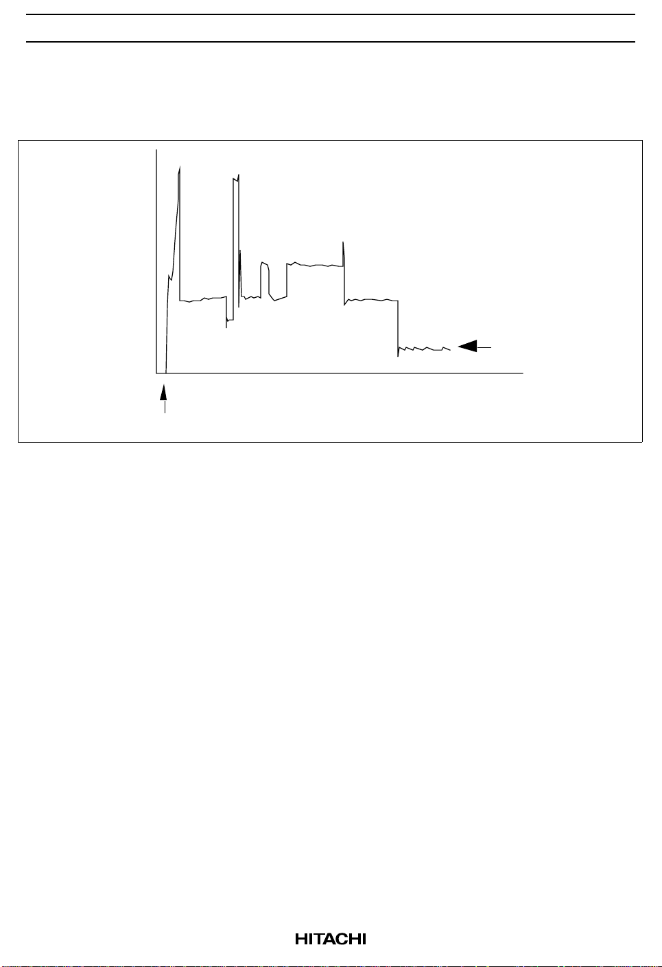
HB288800/640/448/320/256/192/160/128/096/064/032A5
DC Current Waveform (VCC = 5 V, Ta = 25˚C)
Power on Operation (Reference only)
Current
Power on
DC
Time
53
Page 54
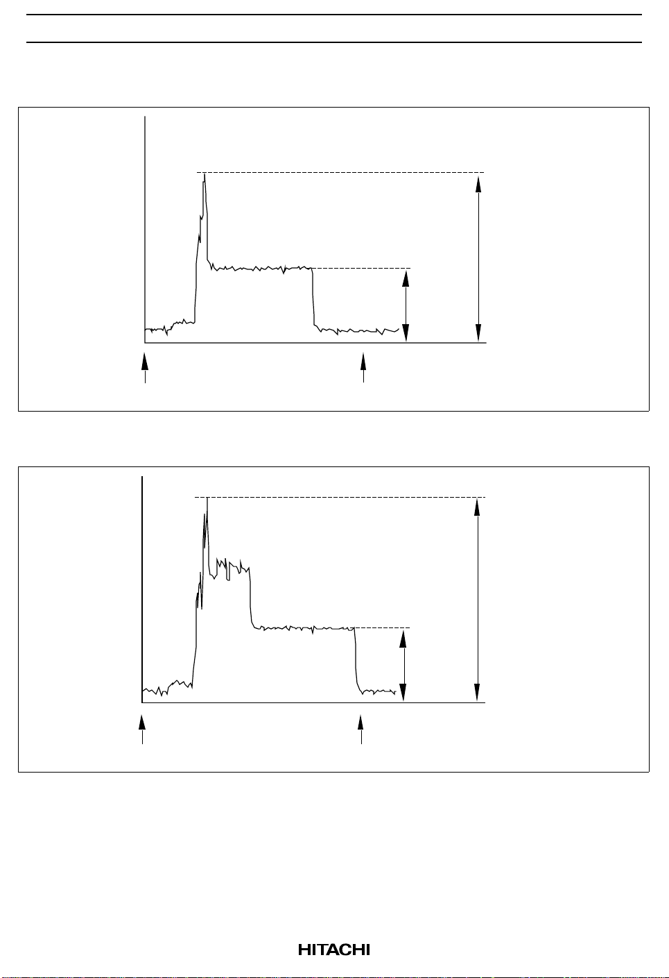
HB288800/640/448/320/256/192/160/128/096/064/032A5
Sector Read
Sector Write
Current
0
Command write
Current
I
CCR(DC)
Complete of sector read
ICCR(Peak)
Time
ICCW(Peak)
54
0
Command write Complete of sector write
CCW(DC)
I
Time
Page 55
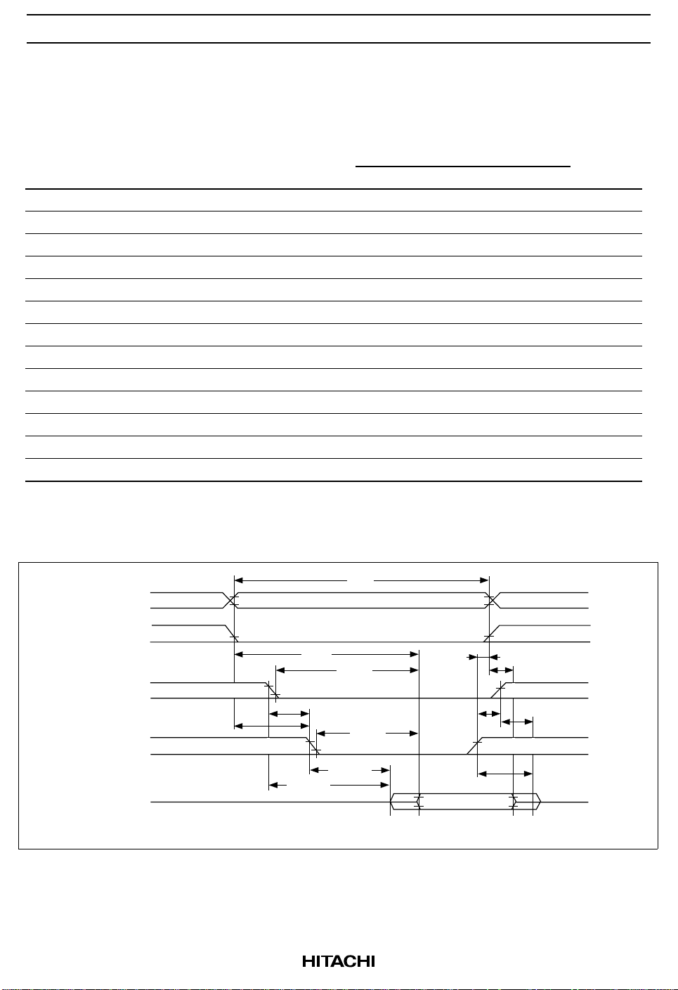
HB288800/640/448/320/256/192/160/128/096/064/032A5
AC Characteristics (Ta = 0 to +60˚C, VCC = 5 V ± 10%, VCC = 3.3 V ±5%)
Attribute Memory Read AC Characteristics
250 ns
Parameter Symbol Min Typ Max Unit
Read cycle time tCR 250 — — ns
Address access time ta(A) — — 250 ns
-CE access time ta(CE) — — 250 ns
-OE access time ta(OE) — — 125 ns
Output disable time (-CE) tdis(CE) — — 100 ns
Output disable time (-OE) tdis(OE) — — 100 ns
Output enable time (-CE) ten(CE) 5 — — ns
Output enable time (-OE) ten(OE) 5 — — ns
Data valid time (A) tv(A) 0 — — ns
Address setup time tsu(A) 30 — — ns
Address hold time th(A) 20 — — ns
-CE setup time tsu(CE) 0 — — ns
-CE hold time th(CE) 20 — — ns
Attribute Memory Read Timing
A0 to A10
-REG
-CE2/-CE1
tsu(A)
-OE
D0 to D15
a(A)
t
t
ten(CE)
ta(CE)
su(CE)
ten(OE)
tCR
ta(OE)
th(A)
th(CE)
Valid Output
-WE, -IOWR, -IORD : High Fix
tv(A)
tdis(CE)
tdis(OE)
55
Page 56
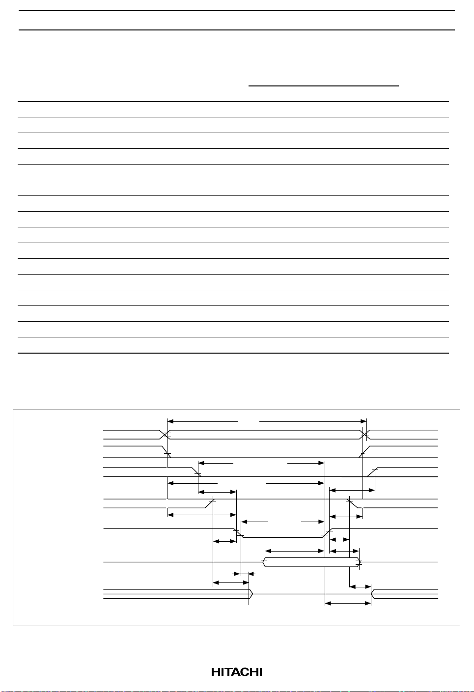
HB288800/640/448/320/256/192/160/128/096/064/032A5
Attribute Memory Write AC Characteristics
250 ns
Parameter Symbol Min Typ Max Unit
Write cycle time tCW 250 — — ns
Write pulse time tw(WE) 150 — — ns
Address setup time tsu(A) 30 — — ns
Address setup time (-WE) tsu(A-WEH) 180 — — ns
-CE setup time (-WE) tsu(CE-WEH) 180 — — ns
Data setup time (-WE) tsu(D-WEH) 80 — — ns
Data hold time th(D) 30 — — ns
Write recover time trec(WE) 30 — — ns
Output disable time (-WE) tdis(WE) — — 100 ns
Output disable time (-OE) tdis(OE) — — 100 ns
Output enable time (-WE) ten(WE) 5 — — ns
Output enable time (-OE) ten(OE) 5 — — ns
Output enable setup time (-WE) tsu(OE-WE) 10 — — ns
Output enable hold time (-WE) th(OE-WE) 10 — — ns
-CE setup time tsu(CE) 0 — — ns
-CE hold time th(CE) 20 — — ns
Attribute Memory Write Timing
A0 to A10
-REG
-CE2/-CE1
-OE
tsu(A)
-WE
D0 to D15(Din)
D0 to D15(Dout)
tsu(OE-WE)
tdis(OE)
tCW
tsu(CE-WEH)
tsu(A-WEH)
tsu(CE)
tw(WE)
tsu(D-WEH)
tdis(WE)
th(CE)
trec(WE)
th(OE-WE)
th(D)
Input Data
ten(OE)
ten(WE)
-IOWR, -IORD : High Fix
56
Page 57
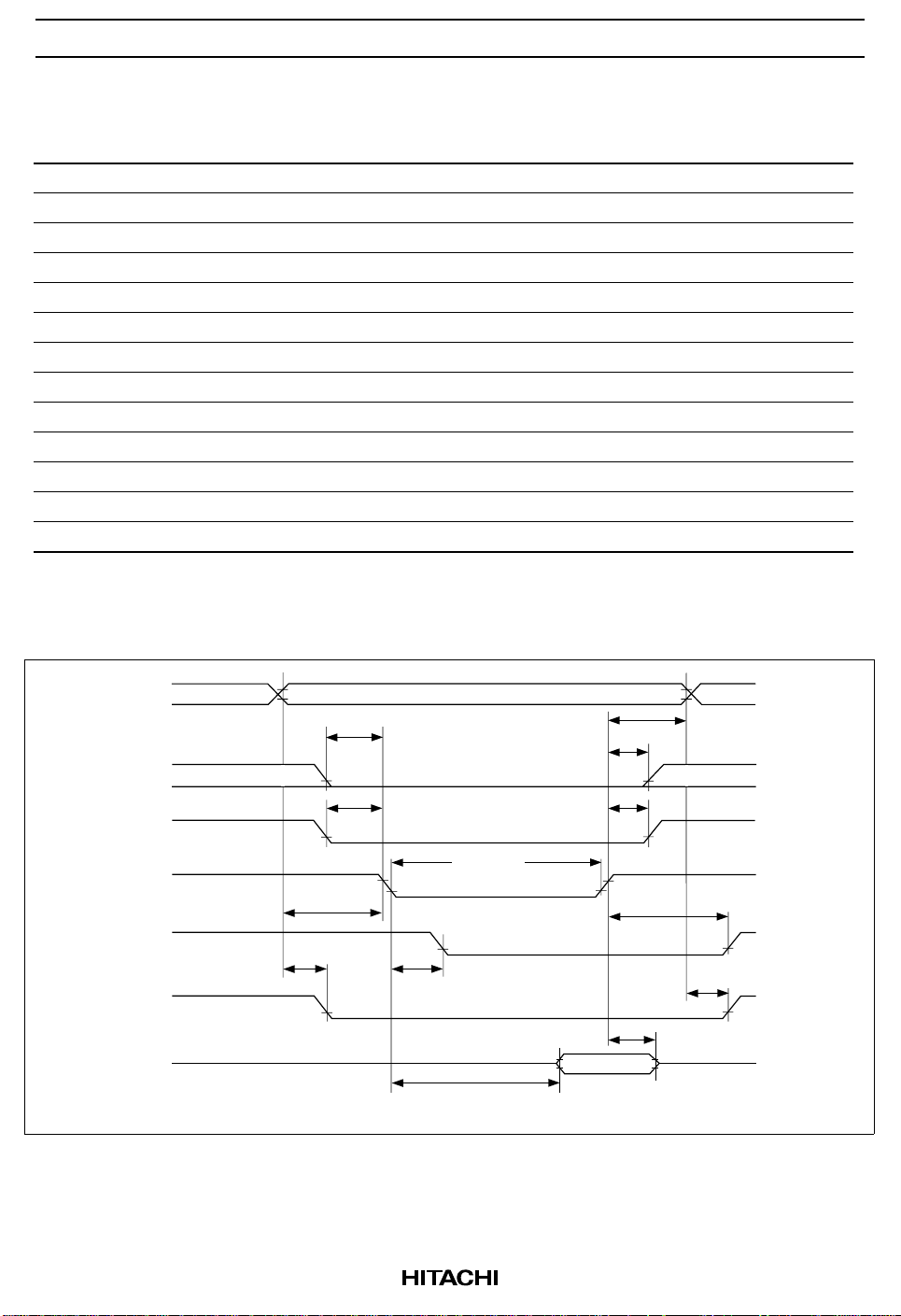
HB288800/640/448/320/256/192/160/128/096/064/032A5
I/O Access Read AC Characteristics
Parameter Symbol Min Typ Max Unit
Data delay after -IORD td(IORD) — — 100 ns
Data hold following -IORD th(IORD) 0 — — ns
-IORD pulse width tw(IORD) 165 — — ns
Address setup before -IORD tsuA(IORD) 70 — — ns
Address hold following -IORD thA(IORD) 20 — — ns
-CE setup before -IORD tsuCE(IORD) 5 — — ns
-CE hold following -IORD thCE(IORD) 20 — — ns
-REG setup before -IORD tsuREG(IORD) 5 — — ns
-REG hold following -IORD thREG(IORD) 0 — — ns
-INPACK delay falling from -IORD tdfINPACK(IORD) 0 — 45 ns
-INPACK delay rising from -IORD tdrINPACK(IORD) — — 45 ns
-IOIS16 delay falling from address tdfIOIS16(ADR) — — 35 ns
-IOIS16 delay rising from address tdrIOIS16(ADR) — — 35 ns
I/O Access Read Timing
A0 to A10
-REG
-CE2/-CE1
-IORD
tsuA(IORD)
-INPACK
tdfIOIS16(ADR)
-IOIS16
D0 to D15
suREG(IORD)
t
tsuCE(IORD)
tw(IORD)
tdfINPACK(IORD)
td(IORD)
thA(IORD)
thREG(IORD)
thCE(IORD)
tdrINPACK(IORD)
tdrIOIS16(ADR)
th(IORD)
Valid Output
-WE, -OE, -IOWR : High Fix
57
Page 58
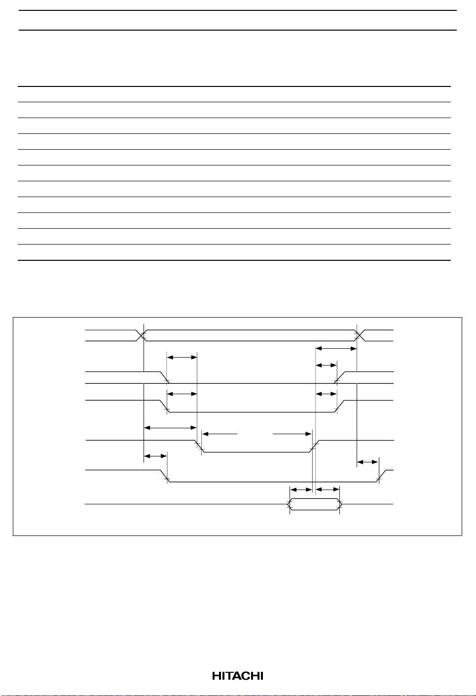
HB288800/640/448/320/256/192/160/128/096/064/032A5
I/O Access Write AC Characteristics
Parameter Symbol Min Typ Max Unit
Data setup before -IOWR tsu(IOWR) 60 — — ns
Data hold following -IOWR th(IOWR) 30 — — ns
-IOWR pulse width tw(IOWR) 165 — — ns
Address setup before -IOWR tsuA(IOWR) 70 — — ns
Address hold following -IOWR thA(IOWR) 20 — — ns
-CE setup before -IOWR tsuCE(IOWR) 5 — — ns
-CE hold following -IOWR thCE(IOWR) 20 — — ns
-REG setup before -IOWR tsuREG(IOWR) 5 — — ns
-REG hold following -IOWR thREG(IOWR) 0 — — ns
-IOIS16 delay falling from address tdfIOIS16(ADR) — — 35 ns
-IOIS16 delay rising from address tdrIOIS16(ADR) — — 35 ns
I/O Access Write Timing
A0 to A10
-REG
-CE2/-CE1
-IOWR
-IOIS16
D0 to D15
tdfIOIS16(ADR)
tsuA(IOWR)
t
suREG(IOWR)
tsuCE(IOWR)
tw(IOWR)
thA(IOWR)
thREG(IOWR)
thCE(IOWR)
tsu(IOWR)
tdrIOIS16(ADR)
th(IOWR)
Data In
-WE, -OE, -IORD : High Fix
58
Page 59
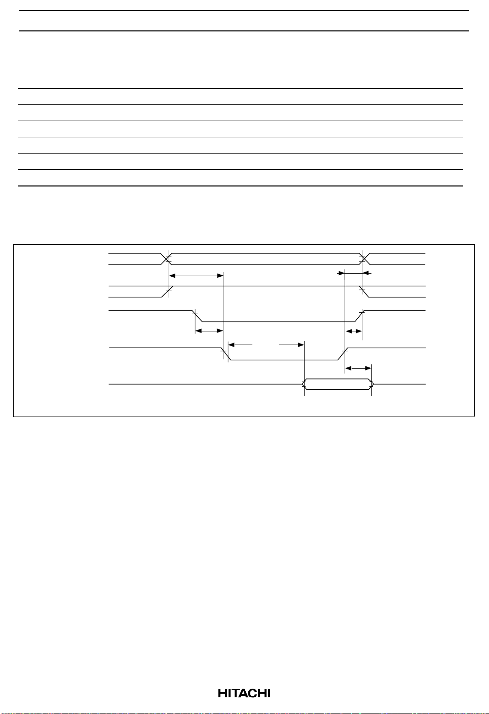
HB288800/640/448/320/256/192/160/128/096/064/032A5
Common Memory Access Read AC Characteristics
Parameter Symbol Min Typ Max Unit
-OE access time ta(OE) — — 125 ns
Output disable time (-OE) tdis(OE) — — 100 ns
Address setup time tsu(A) 30 — — ns
Address hold time th(A) 20 — — ns
-CE setup time tsu(CE) 0 — — ns
-CE hold time th(CE) 20 — — ns
Common Access Read Timing
A0 to A10
th(A)
-REG
su(A)
t
-CE2/-CE1
-OE
D0 to D15
tsu(CE)
th(CE)
ta(OE)
tdis(OE)
Valid Output
-WE, -IORD, -IOWR : High Fix
59
Page 60
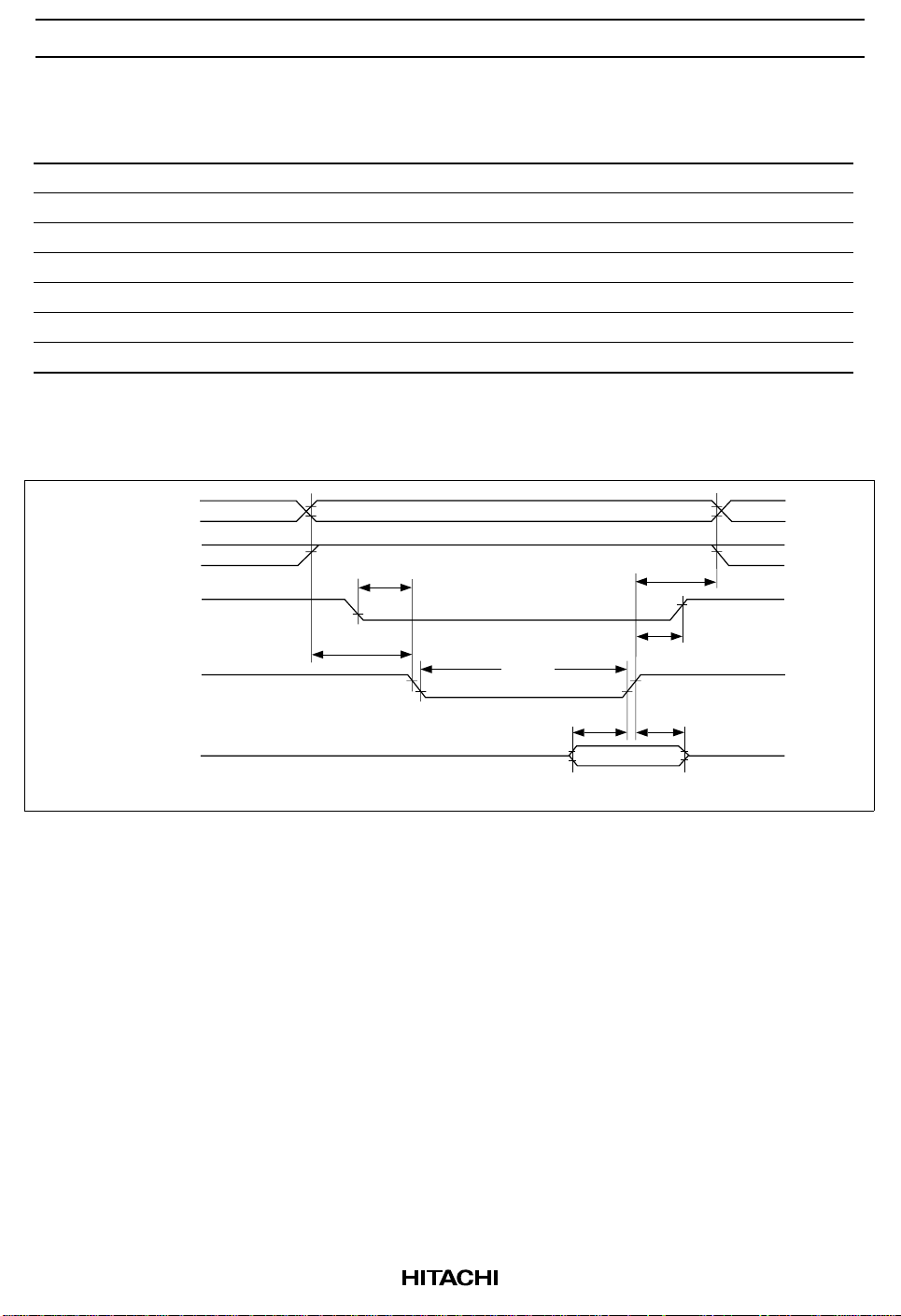
HB288800/640/448/320/256/192/160/128/096/064/032A5
Common Memory Access Write AC Characteristics
Parameter Symbol Min Typ Max Unit
Data setup time (-WE) tsu(D-WEH) 80 — — ns
Data hold time th(D) 30 — — ns
Write pulse time tw(WE) 150 — — ns
Address setup time tsu(A) 30 — — ns
-CE setup time tsu(CE) 0 — — ns
Write recover time trec(WE) 30 — — ns
-CE hold following -WE th(CE) 20 — — ns
Common Access Write Timing
A0 to A10
-REG
-CE2/-CE1
-WE
D0 to D15
tsu(CE)
tsu(A)
tw(WE)
trec(WE)
th(CE)
t
tsu(D-WEH)
-IOWR, -IORD, -OE : High Fix
h(D)
Data In
60
Page 61
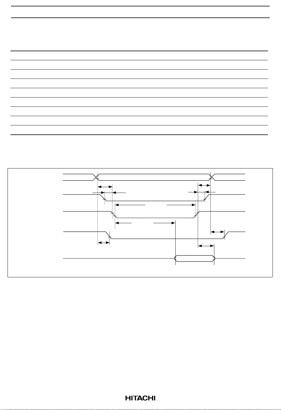
HB288800/640/448/320/256/192/160/128/096/064/032A5
True IDE Mode Access Read AC Characteristics
Parameter Symbol Min Typ Max Unit
data delay after IORD td(IORD) — — 100 ns
data hold following IORD th(IORD) 0 — — ns
IORD width time tw(IORD) 165 — — ns
address setup before IORD tsuA(IORD) 70 — — ns
address hold following IORD thA(IORD) 20 — — ns
CE setup before IORD tsuCE(IORD) 5 — — ns
CE hold following IORD thCE(IORD) 20 — — ns
IOIS16 delay falling from address tdfIOIS16(ADR) — — 35 ns
IOIS16 delay rising from address tdrIOIS16(ADR) — — 35 ns
True IDE Mode Access Read Timing
A0 to A2
thA(IORD)
thCE(IORD)
-CE2/-CE1
-IORD
suA(IORD)
t
tsuCE(IORD)
tw(IORD)
-IOIS16
D0 to D15
tdflOIS16(ADR)
td(IORD)
th(IORD)
Valid Output
-IOWR: High Fix, -OE: Low Fix, -WE: High Fix, A3 to A10: GND
tdrlOIS16(ADR)
61
Page 62
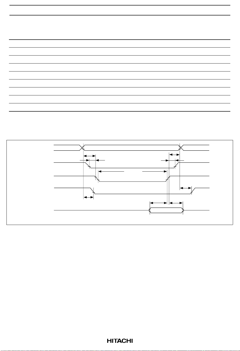
HB288800/640/448/320/256/192/160/128/096/064/032A5
True IDE Mode Access Write AC Characteristics
Parameter Symbol Min Typ Max Unit
Data setup before IOWR tsu(IOWR) 60 — — ns
data hold following IOWR th(IOWR) 30 — — ns
IORD width time tw(IOWR) 165 — — ns
address setup before IOWR tsuA(IOWR) 70 — — ns
address hold following IOWR thA(IOWR) 20 — — ns
CE setup before IOWR tsuCE(IOWR) 5 — — ns
CE hold following IOWR thCE(IOWR) 20 — — ns
IOIS16 delay falling from address tdfIOIS16(ADR) — — 35 ns
IOIS16 delay rising from address tdrIOIS16(ADR) — — 35 ns
True IDE Mode Access Write Timing
A0 to A2
thA(IOWR)
thCE(IOWR)
tsu(IOWR)
tdrlOIS16(ADR)
th(IOWR)
-CE2/-CE1
-IOWR
-IOIS16
tdflOIS16(ADR)
suA(IOWR)
t
tsuCE(IOWR)
tw(IOWR)
62
D0 to D15
Valid Output
-IORD: High Fix, -OE: Low Fix, -WE: High Fix, A3 to A10: GND
Page 63
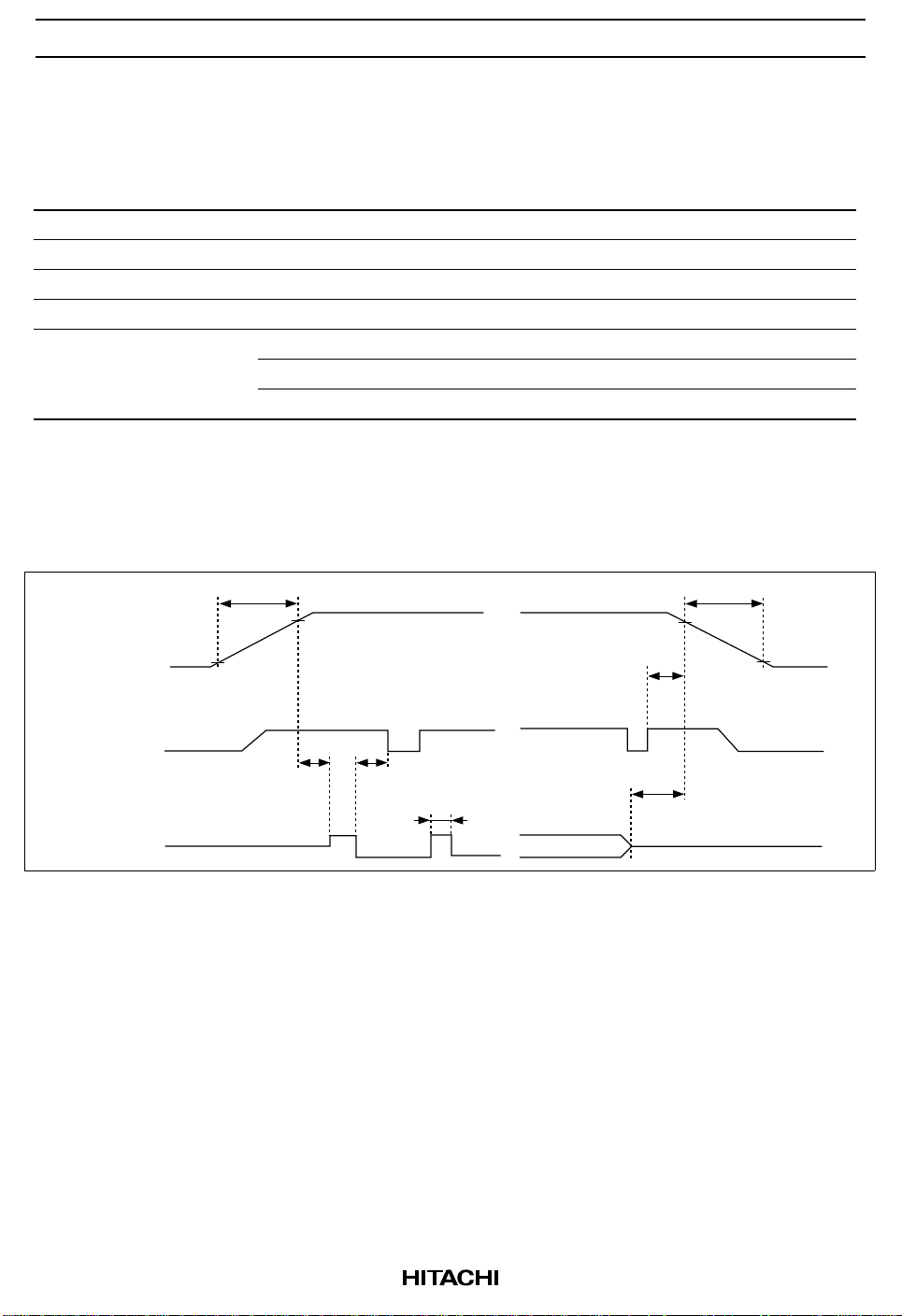
HB288800/640/448/320/256/192/160/128/096/064/032A5
Reset Characteristics (only Memory Card Mode or I/O Card Mode)
Hard Reset Characteristics
Parameter Symbol Min Typ Max Unit Test conditions Note
Reset setup time tsu(RESET) 100 — — ms
-CE recover time trec(VCC) 1 — — µs
VCC rising up time tpr 0.1 — 100 ms
VCC falling down time tpf 3 — 300 ms
Reset pulse width tw(RESET) 10 — — µs
th(Hi-ZRESET) 1 — — ms
ts(Hi-ZRESET) 100 — — ms 1
Note: 1. As for this specification, it is fitted activity state when change. When reset signal is non-activity
state and a card is ready state, can shift to power supply cutoff sequence instantly.
Hard Reset Timing
Vcc
-CE1, -CE2
RESET
t
pr tpf
90%
10%
h(Hi-ZRESET)
t
High-Z High-Z
tsu(RESET)
tw(RESET)
Low
90%
rec(Vcc)
t
ts(Hi-ZRESET)
10%
63
Page 64
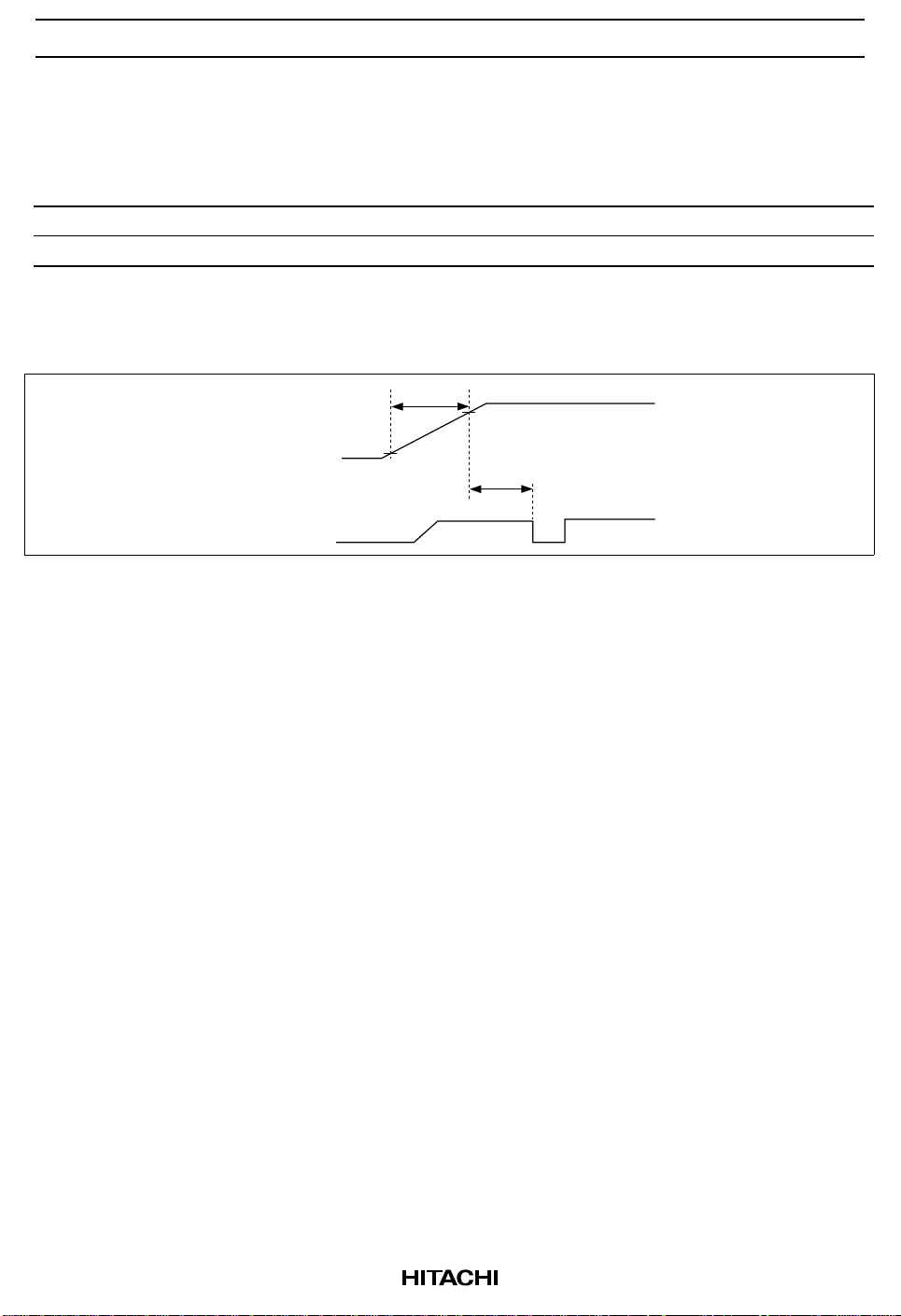
HB288800/640/448/320/256/192/160/128/096/064/032A5
Power on Reset Characteristics
All card status are reset automatically when VCC voltage goes over about 2.3 V.
Parameter Symbol Min Typ Max Unit Test conditions
-CE setup time tsu(VCC) 100 — — ms
VCC rising up time tpr 0.1 — 100 ms
Power on Reset Timing
tpr
Vcc
tsu(vcc)
-CE1, -CE2
Attention for Card Use
• In the reset or power off, all register informations are cleared.
• All card status are cleared automatically when VCC voltage turns below about 2.5V.
• Notice that the card insertion/removal should not be executed during host is active, if the card is used in
True IDE mode.
• After the card hard reset, soft reset, or power on reset, ATA reset, command applied the card cannot
access during +RDY/-BSY pin is "low" level. Flash card can’t be operated in this case.
• Card removal or power off should not be done during internal operations. When the removal or power off
occurred during internal operation, there is the possibility that data are lost.
• Before the card insertion VCC can not be supplied to the card. After confirmation that -CD1, -CD2 pins are
inserted, supply VCC to the card.
• -OE must be kept at the VCC level during power on reset in memory card mode and I/O card mode. -OE
must be kept constantly at the GND level in True IDE mode.
64
Page 65
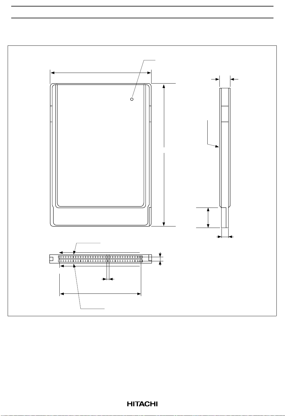
Physical Outline
HB288800/640/448/320/256/192/160/128/096/064/032A5
Unit: mm
Surface A
54.0 ± 0.1
85.6 ± 0.2
5.0 (max)
Surface A
34 pin 1 pin
68 pin
(Reference value)
Surface A
35 pin
1.27 ± 0.1
41.91
Surface B
10.0 min
3.3 ± 0.1
1.27 ± 0.1
65
Page 66

HB288800/640/448/320/256/192/160/128/096/064/032A5
Cautions
1. Hitachi neither warrants nor grants licenses of any rights of Hitachi’s or any third party’s patent,
copyright, trademark, or other intellectual property rights for information contained in this document.
Hitachi bears no responsibility for problems that may arise with third party’s rights, including intellectual
property rights, in connection with use of the information contained in this document.
2. Products and product specifications may be subject to change without notice. Confirm that you have
received the latest product standards or specifications before final design, purchase or use.
3. Hitachi makes every attempt to ensure that its products are of high quality and reliability. However,
contact Hitachi’s sales office before using the product in an application that demands especially high
quality and reliability or where its failure or malfunction may directly threaten human life or cause risk of
bodily injury, such as aerospace, aeronautics, nuclear power, combustion control, transportation, traffic,
safety equipment or medical equipment for life support.
4. Design your application so that the product is used within the ranges guaranteed by Hitachi particularly for
maximum rating, operating supply voltage range, heat radiation characteristics, installation conditions and
other characteristics. Hitachi bears no responsibility for failure or damage when used beyond the
guaranteed ranges. Even within the guaranteed ranges, consider normally foreseeable failure rates or
failure modes in semiconductor devices and employ systemic measures such as fail-safes, so that the
equipment incorporating Hitachi product does not cause bodily injury, fire or other consequential damage
due to operation of the Hitachi product.
5. This product is not designed to be radiation resistant.
6. No one is permitted to reproduce or duplicate, in any form, the whole or part of this document without
written approval from Hitachi.
7. Contact Hitachi’s sales office for any questions regarding this document or Hitachi semiconductor
products.
Hitachi, Ltd.
Semiconductor & Integrated Circuits.
Nippon Bldg., 2-6-2, Ohte-machi, Chiyoda-ku, Tokyo 100-0004, Japan
Tel: Tokyo (03) 3270-2111 Fax: (03) 3270-5109
URL NorthAmerica : http://semiconductor.hitachi.com/
Europe : http://www.hitachi-eu.com/hel/ecg
Asia : http://www.hitachi.com.sg/grp3/sicd
Japan : http://www.hitachi.co.jp/Sicd/indx.htm
For further information write to:
Hitachi Semiconductor
(America) Inc.
179 East Tasman Drive,
San Jose,CA 95134
Tel: <1> (408) 433-1990
Fax: <1>(408) 433-0223
Hitachi Europe GmbH
Electronic Components Group
Dornacher Straße 3
D-85622 Feldkirchen, Munich
Germany
Tel: <49> (89) 9 9180-0
Fax: <49> (89) 9 29 30 00
Hitachi Europe Ltd.
Electronic Components Group.
Whitebrook Park
Lower Cookham Road
Maidenhead
Berkshire SL6 8YA, United Kingdom
Tel: <44> (1628) 585000
Fax: <44> (1628) 585160
Hitachi Asia Ltd.
16 Collyer Quay #20-00
Hitachi Tower
Singapore 049318
Tel: 535-2100
Fax: 535-1533
Hitachi Asia Ltd.
Taipei Branch Office
3rd Flr, Hung Kuo Building, No.167,
Tun Hwa North Road, Taipei (105)
Taiwan
Tel: <886> (2) 2718-3666
Fax: <886> (2) 2718-8180
Telex: 23222 HAS-TP
66
Hitachi Asia (Hong Kong) Ltd.
Group III (Electronic Components)
7th Flr, North Tower, World Finance Centre,
Harbour City, Canton Road, Tsim Sha Tsui,
Kowloon, Hong Kong
Tel: <852> (2) 735 9218
Fax: <852> (2) 730 0281
Telex: 40815 HITEC HX
Copyright © Hitachi, Ltd., 2000. All rights reserved. Printed in Japan.
Colophon 1.0
 Loading...