

Page 1

HB288016MM1
MultiMediaCard
16 MByte
ADE-203-1015B (Z)
Rev. 1.0
Jul. 25, 2000
Description
The Hitachi MultiMediaCard HB288016MM1 is a highly integrated flash memory with serial and
random access capability. It is accessible via a dedicated serial interface optimized for fast and reliable
data transmission. This interface allows several cards to be stacked by through connecting their peripheral
contacts. The HB288016MM1 is fully compatible to a new consumer standard, called the MultiMediaCard
system standard defined in the MultiMediaCard system specification [1]. The MultiMediaCard system is a
new mass-storage system based on innovations in semiconductor technology. It has been developed to
provide an inexpensive, mechanically robust storage medium in card form for multimedia consumer
applications. MultiMediaCard allows the design of inexpensive players and drives without moving parts.
A low power consumption and a wide supply voltage range favors mobile, battery-powered applications
such as audio players, organizers, palmtops, electronic books, encyclopedia and dictionaries. Using very
effective data compression schemes such as MPEG, the MultiMediaCard will deliver enough capacity for
all kinds of multimedia data: software/programs, text, music, speech, images, video etc.
Note: MultiMediaCard is a trademark of Siemens AG.
Features
• 16 MByte memory capacity
• On card error correction
Page 2

HB288016MM1
• MultiMediaCard system standard compatibility
System specification version 2.11 compliant
SPI interface supported
Block and partial block read supported (Command classes 0 and 2)
Stream read supported (Command class 1)
Block write and erase supported (Command classes 4 and 5)
Group write protection (Command classes 6)
Stream write supported (Command classes 3)
Password data access protection
Small erase block size of 512 bytes, tagged erase supported
Read block size programmable between 1 and 2048 bytes
VCC = 2.7 V to 3.6 V operation voltage range (VCC = 2.0 V to 3.6 V for the interface)
No external programming voltage required
Damage free powered card insertion and removal
4kV ESD protection
• High speed serial interface with random access
Read speed: sustained: 13.7 Mbits/s (multi-block read)
burst (one block): 20 Mbit/s
Write speed: sustained: 3.2 Mbit/s (multi-block write to pre-erased sectors)
burst (one block): 20 Mbit/s
Up to 10 stacked card (at 20 MHz, VCC = 2.7 to 3.6V)
Access time: 300 µs (max) (at 20 MHz, VCC = 2.7 to 3.6V, random byte access (Typical case))
• Low power dissipation
High speed: 95 mW (max) (at 20 MHz, VCC = 2.7 V)
2
Page 3
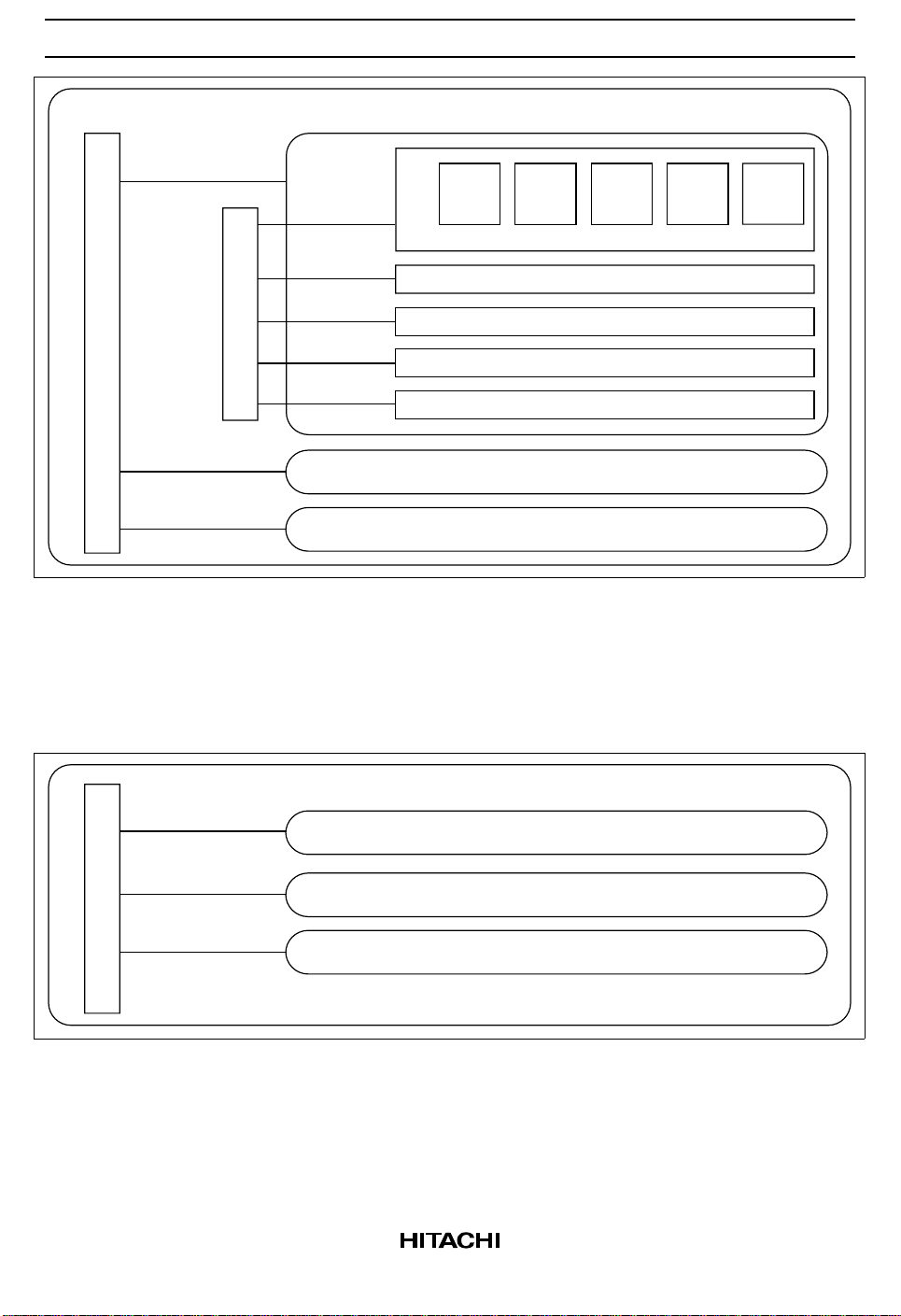
Block Diagram
HB288016MM1
V
PP
Generator
Flash control
1234
V
CC
CS CMD/DI DAT/DOCLK/SCLK
Internal clock
OCR[31:0]
CID[127:0]
set
CSD[127:0]
Register
RCA[15:0]
Interface driver
Interface
Core control
Memory core
567
DA T
CMD
Power on reset unit
All units in the HB288016MM1 are clocked by an internal clock generator. The Interface driver unit
synchronizes the DAT and CMD signals from external CLK to the internal used clock signal. The card is
controlled by the three line MultiMediaCard interface containing the signals: CMD, CLK, DAT (refer to
Chapter “Interfaces”). For the identification of the HB288016MM1 in a stack of MultiMediaCards a card
identification register (CID) and a relative card address register (RCA) is foreseen. An additional register
contains different types of operation parameters. This register is called card specific data register (CSD).
The communication using the MultiMediaCard lines to access either the memory field or the registers is
defined by the MultiMediaCard standard (refer to Chapter “Communication”). The card has its own power
on detection unit. No additional master reset signal is required to setup the card after power on. It is
protected against short circuit during insertion and removal while the MultiMediaCard system is powered
up (refer to Chapter “Power Supply”). No external programming voltage supply is required. The
programming voltage is generated on card. HB288016MM1 supports a second interface operation mode
the SPI interface mode. The SPI mode is activated if the CS signal is asserted (negative) during the
reception of the reset command (CMD0) (refer to Chapter “SPI Communication”).
3
Page 4
HB288016MM1
Interface
The HB288016MM1 interface can operate in two different modes:
• MultiMediaCard mode
• SPI mode
Both modes are using the same pins. The default mode is the MultiMediaCard mode. The SPI mode is
selected by activating (= 0) the CS signal (Pin1) and sending the CMD0.
MultiMediaCard Mode
In the HB288016MM1, all data is transferred over a minimal number of lines:
• CLK: with each cycle of this signal an one bit transfer on the command and data lines is done. The
frequency may vary between zero and the maximum clock frequency. The MultiMediaCard bus master
is free to generate these cycles without restrictions in the range of 0 to 20 MHz.
• CMD: is a bidirectional command channel used for card initialization and data transfer commands.
The CMD signal has two operation modes: open drain for initialization mode and push pull for fast
command transfer. Commands are sent from the MultiMediaCard bus master to the HB288016MM1
and responses vice versa.
• DAT: is a bidirectional data channel with a width of one line. The DAT signal of the HB288016MM1
operates in push pull mode.
Interface driver
R
OD
MultiMediaCard Host
R
DA T
R
CMD
CMD
DA T
CLK
1 2 3 4 5 6 7
HB288016MM1
MultiMediaCard Mode Interface
All MultiMediaCards are connected directly to the lines of the MultiMediaCard bus. The following table
defines the card contacts.
4
Page 5
MultiMediaCard Mode Pad Definition
HB288016MM1
Pin No. Name Type*
1
Description
1 RSV NC No connection
2 CMD I/O/PP/OD Command/Response
3V
SS1
S Ground
4VCCS Power supply
5 CLK I Clock
6V
SS2
S Ground
7 DAT I/O/PP Data
Note: 1. S: power supply; I: input; O: output; PP: push-pull; OD: open-drain; NC: No connection or V
DAT
enable
V
SS2
CLK
IH
V
CC
V
SS1
CMD
1 2 3 4 5 6 7
enable
Interface driver
MultiMediaCard Mode I/O-drivers
MultiMediaCard interface controller
Memory core interface
OD/PP
5
Page 6
HB288016MM1
SPI Mode
The Serial Peripheral Interface (SPI) is a general-purpose synchronous serial interface originally found on
certain Motorola microcontrollers. The MultiMediaCard SPI interface is compatible with SPI hosts
available on the market. As any other SPI device the MultiMediaCard SPI interface consists of the
following four signals:
CS: Host to card Chip Select signal.
CLK: Host to card clock signal
Data in: Host to card data signal.
Data out: Card to host data signal.
The MultiMediaCard card identification and addressing methods are replaced by a hardware Chip Select
(CS) signal. There are no broadcast commands. For every command, a card (slave) is selected by asserting
(active low) the CS signal (refer to Figure “SPI Bus System”). The CS signal must be continuously active
for the duration of the SPI transaction (command, response and data). The only exception occurs during
card programming, when the host can de-assert the CS signal without affecting the programming process.
The bidirectional CMD and DAT lines are replaced by unidirectional data in and data out signals. This
eliminates the ability of executing commands while data is being read or written and, therefore, makes the
sequential and multi block read/write operations obsolete. Only single block read/write commands are
supported by the SPI channel. The SPI interface uses the same seven signals of the standard
MultiMediaCard bus (refer to Table “SPI Interface Pin Configuration”).
Power
supply
SPI bus (CLK, Datain, Dataout)
SPI Bus System
SPI bus master
SPI cardSPI card
CS
CS
6
Page 7

HB288016MM1
SPI Interface Pin Configuration
MuitiMediaCard SPI
Pin No. Name Type*
1
1 RSV NC Reserved for future use CS I Chip select (neg true)
2 CMD I/O/PP/OD Command/Response DI I Data in
3V
SS1
S Ground V
4VCCS Power supply V
5 CLK I Clock SCLK I Clock
6V
SS2
S Ground V
7 DAT I/O/PP Data DO O/PP Data out
Note: 1. S: power supply; I: input; O: output; PP: push-pull; OD: open-drain; NC: No connection or V
Description Name Type Description
SS
CC
SS2
S Ground
S Power supply
S Ground
IH
7
Page 8

HB288016MM1
Registers
The HB288016MM1 contains the following information registers:
Name Width Type Description
OCR 32 Programmed by the
manufacturer.
Read only for user
CID 128 Programmed by the
manufacturer.
Read only for user
RCA 16 Programmed during
initialization, not readable
CSD 128 Programmed by the
manufacturer. Partially
programmable by the user.
CID and RCA are used for identifying and addressing the HB288016MM1. The third register contains the
card specific data record. This record is a set of information fields to define the operation conditions of the
HB288016MM1.
Supported voltage range, card power up status bit
Card identification number, card individual number for
identification.
Relative card address, local system address of a card,
dynamically assigned by the host during initialization.
Card specific data, information about the card operation
conditions.
For the user the CID and the CSD are read only registers. They are read out by special commands (refer to
Chapter “Commands”). The RCA registers are write only registers. Unlike CID and CSD, RCA looses its
contents after powering down the card. Its value is reassigned in each initialization cycle. The
MultiMediaCard registers usage in SPI mode is summarized in Table “MultiMediaCard Registers in SPI
Mode”:
MultiMediaCard Registers in SPI Mode
Name Available in SPI mode Width (Bytes) Description
OCR Yes 32 Operation condition register.
CID Yes 16 Card identification data (serial number, manufacturer ID
etc.)
RCA No
CSD Yes 16 Card specific data, information about the card operation
conditions.
8
Page 9
HB288016MM1
Card Identification (CID)
This register contains the card identification information used during the card identification procedure. It is
a 128 bit wide register, one-time programmable by the provider. The CID is divided into eight slices:
CID Fields
Name Field Width CID-slice
Manufacturer ID MID 8 [127:120]
OEM/Application ID OID 16 [119:104]
Product name PNM 48 [103:56]
Product revision PRV 8 [55:48]
Product serial number PSN 32 [47:16]
Manufacturing date MDT 8 [15:8]
CRC checksum CRC 7 [7:1]
not used, always 1 — 1 [0:0]
The CID has to be error free. To ensure the correctness of the CID a CRC checksum is added to the end of
the CID. The CRC checksum is computed by the following formula:
CRC Calculation: G(x) = x7 + x3 + 1
M(x) = CID[127]∗x
CRC[6...0] = Remainder [(M(x)∗x7)/G(x)]
119
+...+ CID[8]∗x
0
Relative Card Address (RCA)
The 16-bit relative card address register carries the card address assigned by the host during the card
identification. This address is used for the addressed host to card communication after the card
identification procedure. The default value of the RCA register is 0x0001. The value 0x0000 is reserved to
set all cards in Standby State with the command SELECT_DESELECT_CARD (CMD7). The RCA is
programmed with the command SET_RELATIVE_ADDRESS (CMD3) during the initialization procedure.
The content of this register is lost after power down. The default value is assigned when an internal reset is
applied by the power up detection unit of the HB288016MM1.
9
Page 10

HB288016MM1
Card Specific Data (CSD)
The card specific data register describes how to access the card content. The CSD defines card operating
parameters like maximum data access time, data transfer speed.
The CSD Fields
Name Field Width CSD-slice Value Type
CSD structure CSD_STRUCTURE 2 [127:126] 1 read only
Spec version SPEC_VERS 4 [125:122] 2 read only
Reserved — 2 [121:120] 0 read only
Data read access-time-1 TAAC 8 [119:112] 0x0E (1 ms) read only
Data read access-time-2 in
CLK cycles (NAC*100)
Max. data transfer rate TRAN_SPEED 8 [103:96] 0x2A (20 Mbit/s) read only
Card command classes CCC 12 [95:84] 0x0FF (class 0, 1,
Max. read data block length READ_BLK_LEN 4 [83:80] 0x9 (512 bytes) read only
Partial blocks for read
allowed
Write block misalignment WRITE_BLK_MISALIGN1 [78:78] ‘0’ (Disabled) read only
NSAC 8 [111:104] 0x01 (100 cycles) read only
read only
2, 3, 4, 5, 6, 7)
READ_BLK_PARTIAL 1 [79:79] ‘1’*1 (Enabled) read only
Read block misalignment READ_BLK_MISALIGN 1 [77:77] ‘0’ (Disabled) read only
DSR implemented DSR_IMP 1 [76:76] ‘0’ (Disabled) read only
Reserved — 2 [75:74] 0 read only
Device size C_SIZE 12 [73:62] 0x7AB
(16 MByte)*
2
read only
Max. read current at VDD min VDD_R_CURR_MIN 3 [61:59] 0x5 (35 mA) read only
Max. read current at VDD max VDD_R_CURR_MAX 3 [58:56] 0x4 (35 mA) read only
Max. write current at V
Max. write current at V
Device size multiplier C_SIZE_MULT 3 [49:47] 2 (16 MByte)*
min VDD_W_CURR_MIN 3 [55:53] 0x5 (35 mA) read only
DD
max VDD_W_CURR_MAX 3 [52:50] 0x4 (35 mA) read only
DD
3
read only
Erase sector size SECTOR_SIZE 5 [46:42] 0 (512 Bytes) read only
Erase group size ERASE_GRP_SIZE 5 [41:37] 0x0F (8 kByte) read only
10
Page 11

HB288016MM1
Name Field Width CSD-slice Value Type
Write protect group size WP_GRP_SIZE 5 [36:32] 0x01 (16 kByte) read only
Write protect group enable WP_GRP_ENABLE 1 [31:31] ‘1’ read only
Manufacturer default ECC DEFAULT_ECC 2 [30:29] 0 read only
Write speed factor R2W_FACTOR 3 [28:26] 2 (4) read only
Max. write data block length WRITE_BLK_LEN 4 [25:22] 9 (512 Bytes) read only
Partial blocks for write
allowed
Reserved — 5 [20:16] 0 read only
File format group FILE_FORMAT_GRP 1 [15:15] × read/write
Copy flag (OTP) COPY 1 [14:14] ×*
Permanent write protection PERM_WRITE_PROTECT1 [13:13] × read/write
Temporary write protection TMP_WRITE_PROTECT1 [12:12] × read/write/
File format FILE_FORMAT 2 [11:10] × read/write
ECC code ECC 2 [9:8] × read/write/
CRC CRC 7 [7:1] × read/write/
Not used, always 1 — 0 [0:0] 1 read only
Notes: 1. Access time from block to block within sector is 1 µs. For blocks smaller than 256 Byte, it is 62
µs.
2. This field is depended on the model. Refer to also C_SIZE_MULT
3. This field is depended on the model. Refer to also C_SIZE
4. × means user programmable
WRITE_BLK_PARTIAL 1 [21:21] ‘0’ read only
4
read/write
erase
erase
erase
Some of the CSD fields are one-time or multiple programmable by the customer or provider. All other
field values are fixed. The following section describes the CSD fields and their values for the
HB288016MM1:
• CSD_STRUCTURE
CSD Register Structure
CSD_STRUCTURE CSD register structure
‘01’ CSD version No. 1.1
The CSD version of the HB288016MM1 is related to the “MultiMediaCard system specification, Version
2.11”. The parameter CSD_STRUCTURE has permanently the value 1.
11
Page 12

HB288016MM1
• SPEC_VERS
Defines the Spec version supported by the card. It includes the commands set definition and the definition
of the card responses. The card identification procedure is compatible for all spec versions!
SPEC Version
SPEC_VERS System specification version number
‘0010’ System specification version 2.11
The Spec version of the HB288016MM1 is related to the “MultiMediaCard system specification, Version
2.11”. The parameter SPEC_VERS has permanently the value 2.
• TAAC
Defines the asynchronous data access time:
TAAC Access Time Definition
TAAC bit Description Values
2:0 time exponent 0 = 1 ns, 1 = 10 ns, 2 = 100 ns, 3 = 1 µs, 4 = 10 µs,
5 = 100 µs, 6 = 1 ms, 7 = 10 ms
6:3 time mantissa 0 = reserved, 1 = 1.0, 2 = 1.2, 3 = 1.3, 4 = 1.5,
5 = 2.0, 6 = 2.5, 7 = 3.0, 8 = 3.5, 9 = 4.0, A = 4.5,
B = 5.0, C = 5.5, D = 6.0, E = 7.0, F = 8.0
7 reserved always ‘0’
The value for the asynchronous delay for the HB288016MM1 is 1 ms. The coded TAAC value is 0x0E (=
1 ms). For more details refer to Chapter “Operating Characteristics”.
• NSAC
Defines the worst case for the synchronous data access time. NAC is defined as 100*NSAC clock cycles,
where NSAC presents a binary value. Max. value for the data access time NAC is 25.6k clock cycles. The
total access time is the sum of both TAAC and NAC*clock period. The value of NSAC for the
HB288016MM1 is 0x01 (100 cycles). For more details refer to Chapter “Operating Characteristics”.
12
Page 13

HB288016MM1
• TRAN_SPEED
The following table defines the maximum data transfer rate TRAN_SPEED:
Maximum Data Transfer Rate Definition
TRAN_SPEED bit Description
2:0 transfer rate exponent 0 = 100 kbit/s, 1 = 1 Mbit/s, 2 = 10 Mbit/s, 3 = 100
Mbit/s, 4...7 = reserved
6:3 time mantissa 0x0 = reserved, 0x1 = 1.0, 0x2 = 1.2, 0x3 = 1.3, 0x4 = 1.5,
0x5 = 2.0, 0x6 = 2.5, 0x7 = 3.0, 0x8 = 3.5, 0x9 = 4.0, 0xA = 4.5, 0xB = 5.0,
0xC = 5.5, 0xD = 6.0, 0xE = 7.0, 0xF = 8.0
7 reserved = ’0’
The HB288016MM1 supports a transfer rate between 0 and 20 Mbit/s. The parameter TRAN_SPEED is
0x2A.
• CCC
The MultiMediaCard command set is divided into subsets (command classes). The card command class
register CCC defines which command classes are supported by this card. A set CCC bit means that the
corresponding command class is supported. For command class definition refer to Table “HB288016MM1
Command Classes”.
Supported Card Command Classes
CCC bit Supported card command classes
0 class0
1 class1
...... ......
11 class11
The HB288016MM1 supports the command classes 0, 1, 2, 3, 4, 5, 6 and 7. The parameter CCC is
permanently assigned to the value 0x0FF.
13
Page 14

HB288016MM1
• READ_BLK_LEN
The data block length is computed as 2
READ_BLK_LEN
.
Data Block Length
READ_BLK_LEN Block length Remark
0
02
12
...... ......
11 211 = 2048 bytes
12–15 reserved
= 1 byte
1
= 2 bytes
The block length might therefore be in the range 1, 2, 4...2048 bytes. This parameter defines the block
length if READ_BLK_PARTIAL is not set. If READ_BLK_PARTIAL is set this parameter contains the
maximum allowed value of the block length in bytes. All block lengths between one and this value are
permitted. The actual block size is programmed by the command SET_BLOCKLEN (CMD16). The
HB288016MM1 supports block lengths from 1 byte up to 2048 bytes. The parameter READ_BLK_LEN is
permanently assigned to the value 0x9.
• READ_BLK_PARTIAL
READ_BLK_PARTIAL defines whether partial block sizes can be used in block read and block write
commands. READ_BLK_PARTIAL = 0 means that only the block size defined by READ_BLK_LEN can
be used for block-oriented data transfers. READ_BLK_PARTIAL = 1 means that smaller blocks can be
used as well. The minimum block size will be equal to minimum addressable unit (one byte). The
HB288016MM1 supports partial block read. The parameter READ_BLK_PARTIAL is permanently
assigned to the value ‘1’.
• WRITE_BLK_MISALIGN
Defines if the data block to be written by one command can be spread over more than one physical blocks
of the memory device. The size of the memory block is defined in WRITE_BLK_LEN.
WRITE_BLK_MISALIGN is permanently assigned to the value ‘0’, signalling that crossing physical block
boundaries is not allowed.
• READ_BLK_MISALIGN
Defines if the data block to be read by one command can be spread over more than one physical block of
the memory device. The size of the data block is defined in READ_BLK_LEN. READ_BLK_MISALIGN
= 0 signals that crossing physical block boundaries is not allowed. READ_BLK_MISALIGN = 1 signals
that crossing physical block boundaries is allowed. The HB288016MM1 does not support read block
operations with boundary crossing. The parameter READ_BLK_MISALIGN is permanently assigned to
the value ‘0’.
14
Page 15

HB288016MM1
• DSR_IMP
Defines if the configurable driver stage option is integrated on the card or not. If implemented a driver
stage register (DSR) must be implemented also.
DSR Implementation
DSR_IMP DSR type
0 no DSR implemented
1 DSR implemented
The HB288016MM1 output drivers are not configurable. The parameter DSR_IMP is permanently
assigned to the value ‘0’.
• C_SIZE
This parameter is used to compute the card capacity. The memory capacity of the card is computed from
the entries C_SIZE, C_SIZE_MULT and READ_BLK_LEN as follows:
memory capacity = BLOCKNR*BLOCK_LEN
Where
BLOCKNR = (C_SIZE+1)*MULT
MULT = 2
BLOCK_LEN = 2
C_SIZE_MULT+2
READ_BLK_LEN
(C_SIZE_MULT < 8)
, (READ_BLK_LEN < 12)
Therefore, the maximal capacity which can be coded is 4096*512*512 = 1 GBytes.
Example: A 16 MBytes card with BLOCK_LEN = 512 can be coded with C_SIZE_MULT = 2 and
C_SIZE = 1963.
The card capacity is 16 MBytes.
The value of the parameter C_SIZE used in the formula above for the HB288016MM1 is 0x7AB.
15
Page 16

HB288016MM1
• VDD_R_CURR_MIN, VDD_W_CURR_MIN
The maximum supply current at the minimum supply voltage V
Maximum Supply Current Consumption at V
VDD_R_CURR_MIN
VDD_W_CURR_MIN Code for current consumption at 2.7 V
2:0 0 = 0.5 mA; 1 = 1 mA; 2 = 5 mA; 3 = 10 mA; 4 = 25 mA; 5 = 35 mA; 6
= 60 mA; 7 = 100 mA
= 2.7 V
CC
(2.7 V) is coded as follows:
CC
The parameter VDD_R_CURR_MIN and VDD_W_CURR_MIN are permanently assigned to the value 5
(35 mA).
• VDD_R_CURR_MAX, VDD_W_CURR_MAX
The maximum supply current at the maximum supply voltage VCC (3.6 V) is coded as follows:
Maximum Supply Current Consumption at V
VDD_R_CURR_MAX
VDD_W_CURR_MAX Code for current consumption at 3.6 V
2:0 0 = 1 mA; 1 = 5 mA; 2 = 10 mA; 3 = 25 mA; 4 = 35 mA; 5 = 45 mA; 6 =
80 mA; 7 = 200 mA
= 3.6 V
CC
The parameter VDD_R_CURR_MAX and VDD_W_CURR_MAX are permanently assigned to the value 4
(35 mA). For more details refer to Chapter “Characteristics”.
16
Page 17
• C_SIZE_MULT
HB288016MM1
This parameter is used for coding a factor MULT for computing the total device size (refer to “C_SIZE”).
The factor MULT is defined as 2
C_SIZE_MULT+2
.
Multiply Factor for the Device Size
C_SIZE_MULT MULT Remark
2
02
12
22
32
42
52
62
72
= 4
3
= 8
4
= 16
5
= 32
6
= 64
7
= 128
8
= 256
9
= 512
The card capacity is 16 MBytes. The value of the parameter C_SIZE_MULT used in the formula to
calculate the card capacity (refer to parameter “C_SIZE”) for the HB288016MM1 is 2 (multiplier = 16).
• SECTOR_SIZE
The size of an erasable or write protection sector. The content of this register is a binary coded value
defining the number of write blocks (refer to “WRITE_BLK_LEN”) of a sector. The sector size of the
HB288016MM1 is set to 0 (= one write block = 512 bytes).
• ERASE_GROUP_SIZE
The size of an erasable group. The content of this register is a binary coded value defining the number of
sectors (refer to “SECTOR_SIZE”) of a group. This parameters value is 15 which means a group size of
(15+1)*512 bytes = 8 kByte.
• WP_GRP_SIZE
The size of a write protection group. The content of this register is a binary coded value defining the
number of sectors (refer to “SECTOR_SIZE”) of a group. This parameters value is 1 which means a group
size of (1+1)*(ERASE_GROUP_SIZE) = 16 kByte.
• WP_GRP_ENABLE
The value is set to ‘1’, meaning group write protection is enabled.
17
Page 18

HB288016MM1
• DEFAULT_ECC
Set by the card manufacturer and defines the ECC code which is recommended to use (e.g. the device is
tested for). The value is set to ‘0’, indicating that no designated ECC is recommended.
• R2W_FACTOR
Defines the typical block program time as a multiple of the read access time. The following table defines
the field format.
R2W_FACTOR
R2W_FACTOR Multiples of read access time
01
1 2 (write half as fast as read)
24
38
416
532
6, 7 reserved
This parameter value is 2 for the HB288016MM1.
• WRITE_BLK_LEN
The data block length is computed as 2
WRITE_BLK_LEN
.
Data Block Length
WRITE_BLK_LEN Block length Remark
0
02
12
...... ......
11 211 = 2048 bytes
12–15 reserved
= 1 byte
1
= 2 bytes
The block length might therefore be in the range 1, 2, 4...2048 bytes. This parameter defines the block
length if WRITE_BLK_PARTIAL is not set. If WRITE_BLK_PARTIAL is set this parameter contains the
maximum allowed value of the block length in bytes. All block lengths between one and this value are
permitted. The actual block size is programmed by the command SET_BLOCKLEN (CMD16). The
HB288016MM1 supports blocks with the length 512 bytes. The parameter WRITE_BLK_LEN is
permanently assigned to the value 0x9.
18
Page 19

HB288016MM1
• WRITE_BLK_PARTIAL
WRITE_BLK_PARTIAL defines whether partial block sizes can be used in block read and block write
commands. WRITE_BLK_PARTIAL = 0 means that only the block size defined by WRITE_BLK_LEN
can be used for block-oriented data transfers. WRITE_BLK_PARTIAL = 1 means that smaller blocks can
be used as well. The minimum block size will be equal to minimum addressable unit (one byte). The
HB288016MM1 supports no partial block write. The parameter WRITE_BLK_PARTIAL is permanently
assigned to the value ‘0’.
• FILE_FORMAT_GRP
Indicates the selected group of file formats. This field is read-only for ROM. The usage of this field is
shown in table “File_Formats”.
• COPY
Defines if the contents are an original (COPY = “0”) or a copy (= “1”). The COPY bit for OTP and MTP
devices, sold to end consumers, is set to “1” which identifies the card content as a copy. The COPY bit is a
one time programmable bit, being set by the customer
• PERM_WRITE_PROTECT
Permanently protects the whole card content against overwriting or erasing (all write and erase commands
for this card is permanently disabled). This parameter is one-time programmable by the customer. The
default value is ‘0’ (not protected).
• TMP_WRITE_PROTECT
Temporarily protects the whole card content from being overwritten or erased (all write and erase
commands for this card are temporarily disabled). This parameter is programmable by the customer. The
default value is ‘0’ (not protected).
• FILE_FORMAT
Indicates the file format on the card. This field is read-only for ROM. The following formats are defined:
File_Formats
FILE_FORMAT_GRP FILE_FORMAT Type
0 0 Hard disk-like file system with partition table
0 1 DOS FAT (floppy-like) with boot sector only (no partition table)
0 2 Universal File Format
0 3 Others/Unknown
1 0, 1, 2, 3 Reserved
19
Page 20

HB288016MM1
• ECC
Defines the ECC code that was used for storing data on the card. This field is used by the host (or
application) to decode the user data. The following table defines the field format.
ECC Type
ECC ECC type Maximum number of correctable bits
0 none (default) none
1 BCH (542,512) 3
2–15 reserved —
The content provider or customer defines which kind of error correction may be used to protect the contents
of the HB288016MM1. This value is programmable.
• CRC
The CRC register contains the check sum for the CSD content. The check sum is computed by the
following formulas: Generator polynomial:
G(x) = x7 + x3 + 1
119
M(x) = CSD[127]∗x
+...+ CSD[8]∗x0 CRC[6...0] = Remainder [(M(x)∗x7)/G(x)]
The user has to recalculate a new CRC after defining a new CSD.
20
Page 21

HB288016MM1
MultiMediaCard Communication
All communication between host and cards is controlled by the host (master). The host sends commands
and, depending on the command, receives a corresponding response from the selected card. In this chapter
the commands to control the HB288016MM1, the card responses and the contents of the status and error
field included in the responses, are defined.
Memory Array Partitioning
The basic unit of data transfer to/from the MultiMediaCard is one byte. All data transfer operations which
require a block size always define block lengths as integer multiples of bytes. Some special functions need
other partition granularity. For block-oriented commands, the following definition is used:
• Block: is the unit which is related to the block-oriented read and write commands. Its size is the
number of bytes which will be transferred when one block command is sent by the host. The size of a
block is either programmable or fixed. The information about allowed block sizes and the
programmability is stored in the CSD.
For devices which have erasable memory cells, special erase commands are defined. The granularity of the
erasable units is in general not the same as for the block-oriented commands:
• Sector: is the unit which is related to the erase commands. Its size is the number of blocks which will
be erased in one portion. The size of a sector is fixed for each device. The information about the sector
size (in blocks) is stored in the CSD.
• Group: is a number of sectors. Its size is the number of consecutive sectors which will be erased at
once. The size of a group is fixed for each device. The information about the size is stored in the CSD.
For devices which include a write protection:
• WP-Group: is the minimal unit which may have individual write protection. Its size is the number of
sectors which will be write protected by one bit. The size of a WP-group is fixed for each device. The
information about the size is stored in the CSD.
Each erasable unit (group and sector) has a special “tag” bit. This bit may be set or cleared by special
commands to tag the unit. All tagged units will be erased in parallel by one erase command following a
number of tag commands. All tag bits are cleared by each command except a tag or untag command.
Therefore, immediately after a sequence of tag commands an erase command has to be sent by the host.
Commands others than tagging or erasing abort a tag-erase cycle irregularly.
21
Page 22
HB288016MM1
MultiMediaCard
GROUP 0
Block 0 Block 1 Block 2 Block 3 Block n
Sector 0.0
Sector 0.1
Sector 0.2
Sector tagging
Group tagging
GROUP 1
GROUP n
Sector 0.3
Sector 0.n
Erase Tagging Hierarchy
Each WP-group may have an additional write protection bit. The write protection bits are programmable
via special commands (refer to Chapter “Commands”). Both functions are optional and only useful for
writable/erasable devices. The write protection may also be useful for multi type MultiMediaCards (e.g. a
ROM - Flash combination). The information about the availability is stored in the CSD.
WP-GROUP 0
WP-GROUP 1
22
WP-GROUP n
Group write protection
Write Protection
Page 23

HB288016MM1
Commands
The command set of the MultiMediaCard system is divided into classes corresponding to the type of card
(see also [1]). The HB288016MM1 supports the following command classes:
HB288016MM1 Command Classes (Class 0 to Class 2)
Supported commands
Card command
class (CCC) Class description
Class 0 basic ++++++++ +++
Class 1 stream read +
Class 2 block read + + +
HB288016MM1 Command Classes (Class 3 to Class 8)
Card command
class (CCC) Class description
Class 3 stream write +
Class 4 block write ++++
Class 5 erase +++++++
Class 6 write protection + + +
Class 7 lock card +
01234791011121315161718
Supported commands
20 24 25 26 27 28 29 30 32 33 34 35 36 37 38 42
Class 0 is mandatory and supported by all cards. It represents the card identification and initialization
commands, which are intended to handle different cards and card types on the same bus lines. The Card
Command Class (CCC) is coded in the card specific data register of each card, so that the host knows how
to access the card. There are four kinds of commands defined on the MultiMediaCard bus:
• broadcast commands (bc) sent on CMD line, no response
• broadcast commands with response (bcr) sent on CMD line, response (all cards simultaneously) on
CMD line
• addressed (point-to-point) commands (ac) sent on CMD line, response on CMD line
• addressed (point-to-point) data transfer commands (adtc) sent on CMD line, response on CMD line,
data transfer on DAT line
23
Page 24

HB288016MM1
The command transmission always starts with the MSB. Each command starts with a start bit and ends with
a CRC command protection field followed by an end bit. The length of each command frame is fixed to 48
bits (2.4 µs at 20 MHz):
0
start bit1host
Note: 1. (Cyclic Redundancy Check)
bit5...bit0
command
bit31...bit0
argument
bit6...bit0
CRC*
1
1
end bit
The start bit is always ‘0’ in command frames (sent from host to MultiMediaCard). The host bit is always
‘1’ for commands. The command field contains the binary coded command number. The argument
depends on the command (refer to Table “Basic Commands (class 0) and Table “Block-Oriented Read
Commands (class 2)”). The CRC field is defined in Chapter “Cyclic Redundancy Check (CRC)”. The
HB288016MM1 supports the following MultiMediaCard commands:
24
Page 25

HB288016MM1
Read, Write and Erase Time-out Conditions
The times after which a time-out condition for read/write/erase operations occurs are (card indepen-dent)
10 times longer than the access/program times for these operations given below. A card shall complete the
command within this time period, or give up and return an error message. If the host does not get a
response within the defined time-out it should assume the card is not going to respond anymore and try to
recover (e.g. reset the card, power cycle, reject, etc.). The typical access and program times are defined as
follows:
Read
The read access time is defined as the sum of the two times given by the CSD parameters TAAC and
NSAC (refer to Table “Card Specific Data (CSD)”). These card parameters define the typical delay
between the end bit of the read command and the start bit of the data block. This number is card dependent
and should be used by the host to calculate throughput and the maximal frequency for stream read.
Write
The R2W_FACTOR field in the CSD is used to calculate the typical block program time obtained by
multiplying the read access time by this factor. It applies to all write/erase commands (e.g.
SET(CLEAR)_WRITE_PROTECT, PROGRAM_CSD(CID) and the block write commands). It should be
used by the host to calculate throughput and the maximal frequency for stream write.
Erase
The duration of an erase command will be (order of magnitude) the number of sectors to be erased
multiplied by the block write delay.
25
Page 26

HB288016MM1
Basic Commands (class 0) and Read Stream Command (class 1)
CMD
index Type Argument Resp Abbreviation Command description
CMD0 bc [31:0] stuff bits — GO_IDLE_STATE resets all cards to Idle State
CMD1 bcr [31:0] OCR
without busy
CMD2 bcr [31:0] stuff bits R2 ALL_SEND_CID asks all cards in ready state to send
CMD3 ac [31:16] RCA
[15:0] stuff bits
CMD4 bc [31:16] DSR
[15:0] stuff bits
CMD7 ac [31:16] RCA
[15:0] stuff bits
CMD9 ac [31:16] RCA
[15:0] stuff bits
CMD10 ac [31:16] RCA
[15:0] stuff bits
CMD11 adtc [31:0] data
address
CMD12 ac [31:0] stuff bits R1b*
CMD13 ac [31:16] RCA
[15:0] stuff bits
CMD15 ac [31:16] RCA
[15:0] stuff bits
Notes: 1. CID register consists of 128 bits (starting with MSB, it is preceded by an additional start bit, ends
with an end bit)
2. CSD register consists of 128 bits (starting with MSB, it is preceded by an additional start bit,
ends with an end bit)
3. This command is indicating the busy status of the MultiMediaCard via the data channel.
R3 SEND_OP_COND checks for cards not supporting the full
range of 2.0 V to 3.6 V. After receiving
CMD1 the card sends an R3 response
(refer to Chapter “Responses”).
1
numbers on CMD-line
R1 SET_RELATIVE_A
DDR
their CID*
assigns relative address to the card in
identification state.
— SET_DSR programs the DSR of all cards in
stand-by state.
R1 (only
the
selected
card)
SELECT/
DESELECT_CARD
command toggles a card between the
standby and transfer states or between
the programming and disconnect state.
In both cases the card is selected by
its own relative address while
deselecting the prior selected card.
Address 0 deselects all.
R2 SEND_CSD asks the addressed card to send its
card-specific data (CSD)*
2
on CMD-
line.
R2 SEND_CID asks the addressed card to send its
card identification (CID) on CMD- line.
R1 READ_DAT_UNTIL
_STOP
reads data stream from the card,
starting at the given address, until a
STOP_TRANSMISSION follows.
3
STOP_TRANSMIS
forces the card to stop transmission
SION
R1 SEND_STATUS Asks the addressed card to send its
status register.
— GO_INACTIVE_ST
ATE
Sets the card to inactive state in order
to protect the card stack against
communications breakdowns.
26
Page 27

HB288016MM1
Block-Oriented Read Commands (class 2)
CMD
index Type Argument Resp Abbreviation Command description
CMD16 ac [31:0] block
length
CMD17 adtc [31:0] data
address
CMD18 adtc [31:0] data
address
Notes: 1. The default block length is as specified in the CSD.
2. The data transferred must not cross a physical block boundary unless RD_BLK_MISALIGN is
set in the CSD.
Stream Write Command (class 3)
CMD
index Type Argument Resp Abbreviation Command description
CMD20 adtc [31:0] data
address
R1 SET_BLOCKLEN Selects a block length (in bytes) for all
following block commands (read and
1
write).*
R1 READ_SINGLE_BL
OCK
R1 READ_MULTIPLE_
BLOCK
R1 WRITE_DAT_
UNTIL_STOP
Reads a block of the size selected by
the SET_BLOCKLEN command.*
Continuously send blocks of data until
interrupted by a stop.
writes data stream from the host,
starting at the given address, until a
STOP_TRANSMISSION follows.
2
Block-Oriented Write Commands (class 4)
CMD
index Type Argument Resp Abbreviation Command description
CMD24 adtc [31:0] data
address
CMD25 adtc [31:0] data
address
CMD26 adtc [31:0] stuff bits R1 PROGRAM_CID Programming of the card identification
CMD27 adtc [31:0] stuff bits R1 PROGRAM_CSD Programming of the programmable bits
Note: 1. The data transferred must not cross a physical block boundary unless WRITE_BLK_MISALIGN
is set in the CSD.
R1 WRITE_BLOCK Writes a block of the size selected by
the SET_BLOCKLEN command.*
R1 WRITE_MULTIPLE
_ BLOCK
Continuously writes blocks of data until
a STOP_TRANSMISSION follows.
1
register. This command is only done
once per MultiMediaCard card. The
card has some hardware to prevent
this operation after the first
programming. Normally this command
is reserved for the manufacturer.
of the CSD.
27
Page 28

HB288016MM1
Erase Commands (class 5)
CMD
index Type Argument Resp Abbreviation Command description
CMD32 ac [31:0] data
address
CMD33 ac [31:0] data
address
CMD34 ac [31:0] data
address
CMD35 ac [31:0] data
address
CMD36 ac [31:0] data
address
CMD37 ac [31:0] data
address
CMD38 ac [31:0] stuff bits R1b ERASE Erases all previously selected sectors
R1 TAG_SECTOR_ST
ART
R1 TAG_SECTOR_ENDSets the address of the last sector in a
R1 UNTAG_SECTOR Removes one previously selected
R1 TAG_ERASE_GRO
UP_START
R1 TAG_ERASE_GRO
UP_END
R1 UNTAG_ERASE_G
ROUP
Sets the address of the first sector of
the erase group.
continuous range within the selected
erase group to be selected for erase,
or the address of a single sector to be
selected.
sector from the erase selection.
Sets the address of the first erase
group within a range to be selected for
erase
Sets the address of the last erase
group within a continuous range to be
selected for erase
Removes one previously selected
erase group from the erase selection
Write Protection Commands (class 6)
CMD
index Type Argument Resp Abbreviation Command description
CMD28 ac [31:0] data
address
CMD29 ac [31:0] data
address
CMD30 adtc [31:0] write
protect data
address
CMD31 reversed
Note: 1. 32 write protection bits (representing 32 write protect groups starting at the specified address)
followed by 16 CRC bits are transferred in a payload format via the data line. The last (least
significant) bit of the protection bits corresponds to the first addressed group. If the addresses of
the last groups are outside the valid range, then the corresponding write protection bits shall be
set to zero.
R1b SET_WRITE_PROT if the card has write protection
features, this command sets the write
protection bit of the addressed group.
The properties of write protection are
coded in the card specific data
(WP_GRP_SIZE).
R1b CLR_WRITE_PROT if the card provides write protection
features, this command clears the write
protection bit of the addressed group.
R1 SEND_WRITE_PROTif the card provides write protection
features, this command asks the card
to send the status of the write
protection bits.*
1
28
Page 29

HB288016MM1
Lock Card Command (class 7)
CMD
index Type Argument Resp Abbreviation Command description
CMD42 adtc [31:0] stuff bits R1b LOCK_UNLOCK used to set/reset the password or
lock/unlock the card. The size of the
data block is set by the
SET_BLOCK_LEN command.
29
Page 30

HB288016MM1
Card identification mode
All the data communication in the card identification mode uses only the command line (CMD).
Power on
card is busy or
host omitted
voltage range
card looses bus
Idle state
(idle)
CMD1
cards with non-compatible voltage range
Ready state
(ready)
CMD2
Indentification state
(ident)
CMD3
Stand-by state
(stby)
CMD0
Inactive state
(ina)
card wins bus
card-indentification mode
data-transfer mode
from all states except (ina)
CMD15
from all states in data-transfer mode
MultiMediaCard State Diagram (Card Identification Mode)
The host starts the card identification process in open drain mode with the identification clock rate f
OD
(generated by a push pull driver stage). The open drain driver stages on the CMD line allow the parallel
card operation during card identification. After the bus is activated the host will request the cards to send
their valid operation conditions with the command SEND_OP_COND (CMD1). Since the bus is in open
drain mode, as long as there is more than one card with operating conditions restrictions, the host gets in
the response to the CMD1 a “wired or” operation condition restrictions of those cards. The host then must
pick a common denominator for operation and notify the application that cards with out of range
parameters (from the host perspective) are connected to the bus. Incompatible cards go into Inactive State
(refer to also Chapter “Operating Voltage Range Validation”). The busy bit in the CMD1 response can be
used by a card to tell the host that it is still working on its power-up/reset procedure (e.g. downloading the
register information from memory field) and is not ready yet for communication. In this case the host must
repeat CMD1 until the busy bit is cleared. After an operating mode is established, the host asks all cards
for their unique card identification (CID) number with the broadcast command ALL_SEND_CID (CMD2).
All not already identified cards (i.e. those which are in Ready State) simultaneously start sending their CID
numbers serially, while bit-wise monitoring their outgoing bitstream. Those cards, whose outgoing CID
30
Page 31

HB288016MM1
bits do not match the corresponding bits on the command line in any one of the bit periods, stop sending
their CID immediately and must wait for the next identification cycle (cards stay in the Ready State).
There should be only one card which successfully sends its full CID-number to the host. This card then
goes into the Identification State. The host assigns to this card (using CMD3, SET_RELATIVE_ADDR) a
relative card address (RCA, shorter than CID), which will be used to address the card in future
communication (faster than with the CID). Once the RCA is received the card transfers to the Standby
State and does not react to further identification cycles. The card also switches the output drivers from the
open-drain to the push-pull mode in this state. The host repeats the identification process as long as it
receives a response (CID) to its identification command (CMD2). When no card responds to this
command, all cards have been identified. The time-out condition to recognize this, is waiting for the start
bit for more than 5 clock periods after sending CMD2.
Operating Voltage Range Validation
The MultiMediaCard standards operating range validation is intended to support reduced voltage range
MultiMediaCards. The HB288016MM1 supports the range of 2.7 V to 3.6V supply voltage. So the
HB288016MM1 sends a R3 response to CMD1 which contains an OCR value of 0x80FF8000 if the busy
flag is set to “ready” or 0x00FF8000 if the busy flag is active (refer to Chapter “Responses”). By omitting
the voltage range in the command, the host can query the card stack and determine the common voltage
range before sending out-of-range cards into the Inactive State. This bus query should be used if the host is
able to select a common voltage range or if a notification to the application of non usable cards in the stack
is desired. Afterwards, the host must choose a voltage for operation and reissue CMD1 with this condition,
sending incompatible cards into the Inactive State.
31
Page 32

HB288016MM1
Data Transfer Mode
When in Standby State, both CMD and DAT lines are in the push-pull mode. As long as the content of all
CSD registers is not known, the f
PushPull
clock rate is equal to the slow f
OpenDrain
clock rate. SEND_CSD
(CMD9) allows the host to get the Card Specific Data (CSD register), e.g. ECC type, block length, card
storage capacity, maximum clock rate etc..
card-indentification mode
data-transfer mode
CMD13
no state transition
in data-transfer mode
Stand-by state
(stby)
CMD9, 10
''operation
complete''
CMD15 CMD0CMD3
from all states in
data-transfer mode
CMD28, 29, 38
CMD7
CMD7
''operation
complete''
CMD12,
''operation
complete''
CMD24, 25
Sending-data state
(data)
CMD11, 17, 18, 30
Transfer state
(tran)
CMD20, 24, 25, 26, 27, 42
Receive-data state
(rcv)
CMD16, 32...37
Disconnect state
(dis)
CMD7
CMD7
Programming state
(prg)
CMD12 or
''transfer end''
HB288016MM1 State Diagram (Data Transfer Mode)
The command SELECT_DESELECT_CARD (CMD7) is used to select one card and place it in the
Transfer State. If a previously selected card is in the Transfer State its connection with the host is released
and it will move back to the Stand-by State. Only one card can be, at any time, in the Transfer State. A
selected card is responding the CMD7, the deselected one does not respond to this command. When
CMD7 is sent including the reserved relative card address “0x0000”, all cards transfer back to Stand-by
State. This command is used to identify new cards without resetting other already acquired cards. Cards to
which an RCA has already been assigned, do not respond to the identification command flow in this state.
All the data communication in the Data Transfer Mode is consequently a point-to point communication
between the host and the selected card (using addressed commands). All addressed commands are
acknowledged by a response on the CMD line. All read commands (data is sent from the card via data
lines) can be interrupted at any time, by a stop command. The data transfer will terminate and the card will
stop or start working on the next command. The DAT bus line signal level is high when no data is
transmitted. A transmitted data block consists of a start bit (LOW), followed by a continuous data stream.
32
Page 33

HB288016MM1
The data stream contains the net payload data (and error correction bits if an off-card ECC is used). The
data stream ends with an end bit (HIGH). The data transmission is synchronous to the clock signal. The
payload for block-oriented data transfer is preserved by a CRC check sum (refer to Chapter “Cyclic
Redundancy Check (CRC)”).
• Stream read
There is a stream oriented data transfer controlled by READ_DAT_UNTIL_STOP (CMD11). This
command instructs the card to send its payload, starting at a specified address, until the host sends a
STOP_TRANSMISSION command (CMD12). The stop command has an execution delay due to the serial
command transmission. The data transfer stops after the end bit of the stop command. If the end of the
memory range is reached while sending data and no stop command has been sent yet by the host, the
contents of the further transferred payload is undefined. The maximum clock frequency for stream read
operation is given by the following formula:
max. speed = min (TRAN_SPEED, (8*2
these parameters being defined in Chapter “Registers”. If the host attempts to use a higher frequency, the
card may not be able to sustain data transfer. If this happens, the card will set the UNDERRUN error bit in
the status register, abort the transmission and wait in the data state for a stop command.
• Block read
READ_BL_LEN
-NSAC)/TAAC),
The basic unit of data transfer is a block whose maximum size is defined in the CSD (READ_BLK_LEN).
READ_BLK_PARTIAL is set, thus smaller blocks whose starting and ending address are wholly contained
within one physical block (as defined by READ_BLK_LEN) may also be transmitted. A CRC is appended
to the end of each block ensuring data transfer integrity. READ_SINGLE_BLOCK (CMD17) starts a
block read and after a complete transfer the card goes back to Transfer State.
READ_MULTIPLE_BLOCK (CMD18) starts a transfer of several consecutive blocks. Blocks will be
continuously transferred until a stop is issued.
• Stream write
Stream write (CMD20) starts the data transfer from the host to the card beginning from the starting address
until the host issues a stop command. If partial blocks are allowed (if CSD parameter
WRITE_BL_PARTIAL is set) the data stream can start and stop at any address within the card address
space, otherwise it shall start and stop only at block boundaries. Since the amount of data to be transferred
is not determined in advance, CRC can not be used. If the end of the memory range is reached while
sending data and no stop command has been sent by the host, all further transferred data is discarded. The
maximum clock frequency for stream write operation is given by the following formula:
max. speed = min ( TRAN_SPEED, (8*2
WRITE_BL_LEN
-NSAC)/(TAAC*R2W_FACTOR)),
these parameters being defined in Chapter “Registers”. If the host attempts to use a higher frequency, the
card may not be able to process the data and will stop programming, set the OVERRUN error bit in the
status register, and while ignoring all further data transfer, wait (in the Receive-data-State) for a stop
command. The write operation shall also be aborted if the host tries to write over a write-protected area. In
this case, however, the card shall set the WP_VIOLATION bit.
33
Page 34

HB288016MM1
• Block write
Block write (CMD24 - 27) means that one or more blocks of data are transferred from the host to the card
with a CRC appended to the end of each block by the host. A card supporting block write must always be
able to accept a block of data defined by WRITE_BLK_LEN. If the CRC fails, the card will indicate the
failure on the DAT line; the transferred data will be discarded and not written and all further transmitted
blocks (in multiple block write mode) will be ignored. If the host uses partial blocks whose accumulated
length is not block aligned and block misalignment is not allowed (CSD parameter
WRITE_BLK_MISALIGN is not set), the card will detect the block misalignment error and abort
programming before the beginning of the first misaligned block. The card will set the ADDRESS_ERROR
error bit in the status register, and wait (in the Receive-data-State) for a stop command while ignoring all
further data transfer. The write operation will also be aborted if the host tries to write over a writeprotected area. In this case, however, the card will set the WP_VIOLATION bit. Programming of the CID
and CSD register does not require a previous block length setting. The transferred data is also CRC
protected. The HB288016MM1 write operation follows some special rules:
• Write to erased cells is done without automatic erase
• Write to non-erased cells can be done by sending a previous erase command
• Write to non-erased cells without a previous erase command enforces the card to erase before
writing automatically (“rewrite”)
• Erase
It is desirable to erase as many sectors at a time as possible in order to enhance the data throughput.
Identification of these sectors is accomplished with the TAG_* commands. Either an arbitrary set of
sectors within a single erase group, or an arbitrary selection of erase groups may be erased at one time, but
not both together. That is, the unit of measure for determining an erase is either a sector or an erase group,
but if a sector, all selected sectors must lie within the same erase group. To facilitate selection, a first
command with the starting address is followed by a second command with the final address, and all sectors
within this range will be selected for erase. After a range is selected, an individual sector (or group) within
that range can be removed using the UNTAG command. The host must adhere to the following command
sequence; TAG_SECTOR_START, TAG_SECTOR_END, UNTAG_SECTOR (up to 16 untag sector
commands can be sent for one erase cycle) and ERASE (or the same sequence for group tagging). The
following exception conditions are detected by the card: An erase or tag/untag command is received out of
sequence. The card will set the ERASE_SEQUENCE error bit in the status register and reset the whole
sequence. An out of sequence command (except SEND_STATUS) is received. The card will set the
ERASE_RESET status bit in the status register, reset the erase sequence and execute the last command. If
the erase range includes write protected sectors, they will be left intact and only the non-protected sectors
will be erased. The WP_ERASE_SKIP status bit in the status register will be set. The address field in the
tag commands is a sector or a group address in byte units. The card will ignore all LSB’s below the group
or sector size. The number of untags commands (CMD34 and CMD37) which are used in a sequence is
limited up to 16. As described above for block write, the card will indicate that an erase is in progress by
holding DAT low. The actual erase time may be quite long, and the host may choose to deselect the card
using CMD7.
34
Page 35

HB288016MM1
• Write protect management
Card data may be protected against either erase or write. The entire card may be permanently write
protected by the manufacturer or content provider by setting the permanent or temporary write protect bits
in the CSD. Portions of the data may be protected (in units of WP_GRP_SIZE sectors as specified in the
CSD), and the write protection may be changed by the application. The SET_WRITE_PROT command
sets the write protection of the addressed write-protect group, and the CLR_WRITE_PROT command
clears the write protection of the addressed write-protect group. The SEND_WRITE_PROT command is
similar to a single block read command. The card shall send a data block containing 32 write protection
bits (representing 32 write protect groups starting at the specified address) followed by 16 CRC bits. The
address field in the write protect commands is a group address in byte units. The card will ignore all LSB’s
below the group size.
• Card lock/unlock operation
The password protection feature enables the host to lock a card while providing a password, which later
will be used for unlocking the card. The password and its size are kept in a 128-bit PWD and 8-bit
PWD_LEN registers, respectively. These registers are non-volatile so that a power cycle will not erase
them. Locked cards respond to (and execute) all commands in the "basic" command class (class 0) and
“lock card” command class. Thus the host is allowed to reset, initialize, select, query for status, etc., but
not to access data on the card. If the password was previously set (the value of PWD_LEN is not‘0’) will
be locked automatically after power on. Similar to the existing CSD and CID register write commands the
lock/unlock command is available in "transfer state" only. This means that it does not include an address
argument and the card has to be selected before using it. The card lock/unlock command has the structure
and bus transaction type of a regular single block write command. The transferred data block includes all
the required information of the command (password setting mode, PWD itself, card lock/unlock etc.). The
following table describes the structure of the command data block.
Lock Card Data Structure
Byte# Bit7 Bit6 Bit5 Bit4 Bit3 Bit2 Bit1 Bit0
0 Reserved ERASE LOCK_
UNLOCK
1 PWD_LEN
2 Password data
...
PWD_LEN + 1
CLR_
PWD
SET_
PWD
• ERASE: 1 Defines Forced Erase Operation (all other bits shall be ‘0’) and only the cmd byte is
sent.
• LOCK/UNLOCK: 1 = Locks the card. 0 = Unlock the card (note that it is valid to set this bit
together with SET_PWD but it is not allowed to set it together with CLR_PWD).
• CLR_PWD: 1 = Clears PWD.
• SET_PWD: 1 = Set new password to PWD
• PWD_LEN: Defines the following password length (in bytes).
35
Page 36

HB288016MM1
• PWD: The password (new or currently used depending on the command).
The data block size shall be defined by the host before it sends the card lock/unlock command. This will
allow different password sizes. The following paragraphs define the various lock/unlock command
sequences:
• Setting the Password
—Select a card (CMD7), if not previously selected already
—Define the block length (CMD16), given by the 8bit card lock/unlock mode, the 8-bit password
size (in bytes), and the number of bytes of the new password. In case that a password replacement
is done, then the block size shall consider that both passwords, the old and the new one, are sent
with the command.
—Send Card Lock/Unlock command with the appropriate data block size on the data line
including 16 bit CRC. The data block shall indicate the mode (SET_PWD), the length
(PWD_LEN) and the password itself. In case that a password replacement is done, then the length
value (PWD_LEN) shall include both passwords, the old and the new one, and the PWD field
shall include the old password (currently used) followed by the new password.
—In case that the sent old password is not correct (not equal in size and content) then
LOCK_UNLOCK_FAILED error bit will be set in the status register and the old password
password and its size will be saved in the PWD and PWD_LEN fields, respectively.
Note that the password length register (PWD_LEN) indicates if a password is currently set. When it equals
‘0’ there is no password set. If the value of PWD_LEN is not equal to zero the card will lock itself after
power up. It is possible to lock the card immediately in the current power session by set-ting the
LOCK/UNLOCK bit (while setting the password) or sending additional command for card lock.
• Reset the Password:
—Select a card (CMD7), if not previously selected already
—Define the block length (CMD16), given by the 8 bit card lock/unlock mode, the 8 bit password
size (in bytes), and the number of bytes of the currently used password.
—Send the card lock/unlock command with the appropriate data block size on the data line
including 16 bit CRC. The data block shall indicate the mode CLR_PWD, the length
(PWD_LEN) and the password (PWD) itself (LOCK/UNLOCK bit is don’t care). If the PWD
and PWD_LEN content match the sent password and its size, then the content of the PWD
register is cleared and PWD_LEN is set to 0. If the password is not correct then the
LOCK_UNLOCK_FAILED error bit will be set in the status register.
• Locking a card:
—Select a card (CMD7), if not previously selected already
—Define the block length (CMD16), given by the 8 bit card lock/unlock mode, the 8 bit
password size (in bytes), and the number of bytes of the currently used password.
36
Page 37

HB288016MM1
—Send the card lock/unlock command with the appropriate data block size on the data
line including 16 bit CRC. The data block shall indicate the mode LOCK, the length
(PWD_LEN) and the password (PWD) itself.
If the PWD content equals to the sent password then the card will be locked and the card-locked status bit
will be set in the status register. If the password is not correct then LOCK_UNLOCK_FAILED error bit
will be set in the status register. Note that it is possible to set the password and to lock the card in the same
sequence. In such case the host shall perform all the required steps for setting the password (as described
above) including the bit LOCK set while the new password command is sent. If the password was
previously set (PWD_LEN is not ‘0’), then the card will be locked automatically after power on reset. An
attempt to lock a locked card or to lock a card that does not have a password will fail and the
LOCK_UNLOCK_FAILED error bit will be set in the status register.
• Unlocking the card:
—Select a card (CMD7), if not previously selected already.
—Define the block length (CMD16), given by the 8 bit card lock/unlock mode, the 8 bit
password size (in bytes), and the number of bytes of the currently used password.
—Send the card lock/unlock command with the appropriate data block size on the data
line including 16 bit CRC. The data block shall indicate the mode UNLOCK, the length
(PWD_LEN) and the password (PWD) itself.
If the PWD content equals to the sent password then the card will be unlocked and the card-locked status
bit will be cleared in the status register. If the password is not correct then the LOCK_UNLOCK_FAILED
error bit will be set in the status register. Note that the unlocking is done only for the current power
session. As long as the PWD is not cleared the card will be locked automatically on the next power up.
The only way to unlock the card is by clearing the password. An attempt to unlock an unlocked card will
fail and LOCK_UNLOCK_FAILED error bit will be set in the status register.
• Forcing Erase:
In case that the user forgot the password (the PWD content) it is possible to erase all the card data content
along with the PWD content. This operation is called Forced Erase.
—Select a card (CMD7), if not previously selected already.
—Define the block length (CMD16) to 1 byte (8bit card lock/unlock command). Send
the card lock/unlock command with the appropriate data block of one byte on the data
line including 16 bit CRC. The data block shall indicate the mode ERASE (the ERASE
bit shall be the only bit set).
If the ERASE bit is not the only bit in the data field then the LOCK_UNLOCK_FAILED error bit will be
set in the status register and the erase request is rejected. If the command was accepted then ALL THE
CARD CONTENT WILL BE ERASED including the PWD and PWD_LEN register content and the
locked card will get unlocked. An attempt to force erase on an unlocked card will fail and
LOCK_UNLOCK_FAILED error bit will be set in the status register.
37
Page 38

HB288016MM1
• State transition summary
Table “Card State Transition Table” defines the card state transitions as a function of received command
Card State Transition Table
Current state
Command idle ready ident stby tran data rcv prg dis ina
CRC fail —*1—————————
Commands out of the
supported class(es)
Class0 CMD0 idle idle idle idle idle idle idle idle idle —
CMD1, card V
range compatible
CMD1, card is
busy
CMD1, card V
range not
compatible
CMD2, card wins
bus
CMD2, card loses
bus
CMD3 — — stby ———————
CMD4 — — — stby ——————
CMD7, card is
addressed
CMD7, card is not
addressed
CMD9 — — — stby ——————
CMD10 — — — stby ——————
CMD12 ————× tran prg ××—
CMD13 — — — stby tran data rcv prg dis —
CMD15 — — — ina ina ina ina ina ina —
Class1 CMD11 ————data —————
Class2 CMD16 ————tran ×××——
CMD17 ————data ×××——
CMD18 ————data ×××——
Class3 CMD20 ————rcv—————
——————————
ready —————————
CC
idle —————————
ina—————————
CC
— ident ————————
— ready ————————
— — — tran ×*
2
×××prg —
————stby stby — dis — —
38
Page 39

HB288016MM1
Current state
Command idle ready ident stby tran data rcv prg dis ina
Class4 CMD24 ————rcv××rcv — —
CMD25 ————rcv××rcv — —
CMD26 ————rcv×××——
CMD27 ————rcv×××——
Class5 CMD32 ————tran ×××——
CMD33 ————tran ×××——
CMD34 ————tran ×××——
CMD35 ————tran ×××——
CMD36 ————tran ×××——
CMD37 ————tran ×××——
CMD38 ————prg×××——
Class6 CMD28 ————prg×××——
CMD29 ————prg×××——
CMD30 ————data ×××——
Class7 CMD42 ————rcv—————
Notes: 1. “—” means command is ignored, no state change and no response.
2. “×” means “illegal command”, no state change and bit 22 (ILLEGAL_COMMAND) of the status
word de-fined in Chapter “Status” is set in the corresponding response.
39
Page 40

HB288016MM1
Responses
All responses are sent via command line (CMD), all data starts with the MSB.
Format R1 (response command): response length 48 bit.
0
start bit0card
bit5...bit0
command
bit31...bit0
status
bit6...bit0
CRC
1
end bit
The contents of the status field are described in Chapter “Status”
Format R1b (response command with busy signal):
R1b is identical to R1 with an optional busy signal transmitted on the data line. The card may become
busy after receiving these commands based on its state prior to the command reception.
Format R2 (CID, CSD register): response length 136 bits.
Note: Bit 127 down to bit 1 of CID and CSD are transferred, the reserved bit [0] is replaced by the end bit.
0
start bit0card
bit5...bit0
reserved
bit127...bit1
CID or CSD register
including internal CRC
1
end bit
CID register is sent as a response to commands CMD2 and CMD10.
CSD register is sent as a response to the CMD9.
Format R3 (OCR): response length 48 bits.
0
start bit0card
bit5...bit0
reserved
bit31...bit0
OCR field
bit6...bit0
reserved
1
end bit
The OCR is sent as a response to the CMD1 to signalize the supported voltage range. The HB288016MM1
supports the range from 2.7 V to 3.6 V. Respectively the value of all bits of the OCR field of the
HB288016MM1 is set to 0x80FF8000. So the R3 frame of the HB288016MM1 contains the value
0x3F80FF8000FF if the card is ready and 0x3F00FF8000FF if the card is busy.
40
Page 41

HB288016MM1
Status
The response format R1 contains a 32-bit field with the name card status. This field is intended to transmit
status information which is stored in a local status register of each card to the host. The following table
defines the status register structure. The Type and Clear-Condition fields in the table are coded as follows:
• Type:
• E: Error bit.
• S: Status bit.
• R: Detected and set for the actual command response.
• X: Detected and set during command execution. The host must poll the card by sending status
command in order to read these bits.
• Clear Condition:
• A: According to the card state.
• B: Always related to the previous command. Reception of a valid command will clear it (with a
delay of one command).
• C: Clear by read.
41
Page 42

HB288016MM1
Status
Bits Identifier Type Value Description Clear condition
31 OUT_OF_RANGE E R ’0’= no error
’1’= error
30 ADDRESS_ERROR E R X ’0’= no error
’1’= error
29 BLOCK_LEN_ERRORE R ’0’= no error
’1’= error
28 ERASE_SEQ_ERRORE R ’0’= no error
’1’= error
27 ERASE_PARAM E X ’0’= no error
’1’= error
26 WP_VIOLATION E R X ’0’= not protected
’1’= protected
25 CARD_IS_LOCKED S X ’0’= card
unlocked
’1’= card locked
24 LOCK_UNLOCK_
FAILED
23 COM_CRC_ERROR E R ’0’= no error
22 ILLEGAL_COMMANDE R ’0’= no error
21 CARD_ECC_FAILEDE X ’0’= success
20 CC_ERROR E R X ’0’= no error
19 ERROR E R X ’0’= no error
18 UNDERRUN E X ’0’= no error
17 OVERRUN E X ’0’= no error
E R X ’0’= no error
’1’= error
’1’= error
’1’= error
’1’= failure
’1’= error
’1’= error
’1’= error
’1’= error
The commands argument was out
of allowed range for this card.
A misaligned address, which did
not match the block length was
used in the command.
The transferred block length is not
allowed for this card or the
number of transferred bytes does
not match the block length
An error in the sequence of erase
commands occurred.
An invalid selection, sectors or
groups, for erase.
The command tried to write a
write protected block.
When set, signals that the card is
locked by the host.
Set when a sequence or
password error has been detected
in lock/unlock card command or it
there was an attempt to access a
locked card.
The CRC check of the previous
command failed.
Command not legal for the current
state
Card internal ECC was applied
but the correction of data is failed.
Internal card controller error C
A general or an unknown error
occurred during the operation.
The card could not sustain data
transfer in stream read mode.
The card could not sustain data
programming in stream write
mode.
C
C
C
C
C
C
A
C
B
B
C
C
C
C
42
Page 43

HB288016MM1
Bits Identifier Type Value Description Clear Condition
16 CID_OVERWRITE/
CSD_OVERWRITE
E R X ’0’= no error
’1’= error
can be either one of the following
errors:
• The CID register is already
written and can not be
overwritten.
• The read only section of the
CSD does not match the card
content.
• An attempt to reversecopy (set
as original) or permanent WP
(unprotect) bits was done.
C
15 WP_ERASE_SKIP S X ’0’= not protected
’1’= protected
14 CARD_ECC_
DISABLED
13 ERASE_RESET S R ’0’= cleared
12:9 CURRENT_STATE S X 0 = idle
8 BUFFER_EMPTY S X ’0’= not empty
7:6 reserved Permanently 0
5 APP_CMD S R ’0’= disabled
4 reserved Permanently 0
3:2 reserved for application specific commands
1:0 reserved for manufacturer test mode
S X ’0’= enabled
’1’= disabled
’1’= set
1 = ready
2 = ident
3 = stby
4 = tran
5 = data
6 = rcv
7 = prg
8 = dis
9-15 = reserved
’1’= empty
’1’= enabled
Only partial address space was
erased due to existing WP blocks.
The command has been executed
without using the internal ECC.
An erase sequence was cleared
before executing because an out
of erase sequence command was
received
Current state of the card. B
corresponds to buffer empty
signalling on the bus
The card will expect ACMD or
indication that the command has
been interpreted as ACMD.
C
A
C
A
C
43
Page 44

HB288016MM1
Command Response Timings
All timing diagrams use the following schematics and abbreviations:
S: Start bit (= 0)
T: Transmitter bit (Host = 1, Card = 0)
P: One-cycle pull-up (= 1)
E: End bit (= 1)
Z: high impedance state (-> = 1)
D: Data bits
*: repeater
CRC: Cyclic redundancy check bits (7 bits)
The difference between the P-bit and Z-bit is that a P-bit is actively driven to HIGH by the card
respectively host output driver, while the Z-bit is driven to (respectively kept) HIGH by the pull-up
resistors R
timing of the HB288016MM1, the following values are defined:
respectively R
CMD
. Actively driven P-bits are less sensitive to noise superposition. For the
DAT
Timing Values
Value [clock cycles]
Symbol Min Max Description
N
CR
N
ID
N
AC
N
RC
N
CC
N
WR
Notes: 1. Refer to Chapter “Electrical Characteristics” for more details about the access time.
2. Refer to Chapter “Time-out Condition”.
2 64 Number of cycles between command and
response
5 5 Number of cycles between card identification
or card operation conditions command and the
corresponding response
1
2*
TAAC + NSAC*2Number of cycles between a command and
the start of a related data block
8 — Number of cycles between the last response
and a new command
8 — Number of cycles between two commands, if
no response will be sent after the first
command (e.g. broadcast)
2 — Number of cycles between a write command
and the start of a related data block
44
Page 45

HB288016MM1
The host command and the card response are clocked out with the rising edge of the host clock. The delay
between host command and card response is NCR clock cycles. The following timing diagram is relevant
for host command CMD3:
CMD
Host command
S T content CRC E Z * * * * * * Z
Host active
S T content CRC E Z Z Z
ResponseNCR cycles
Card active
Command Response Timing (Identification Mode)
There is just one Z bit period followed by P bits pushed up by the responding card. The following timing
diagram is relevant for all host commands followed by a response, except CMD1, CMD2 and CMD3:
CMD
Host command
S T content CRC E Z Z P * * * P
Host active
NCR cycles
S T content CRC E Z Z Z
Response
Card active
Command Response Timing (Data Transfer Mode)
• Card identification and card operation conditions timing
The card identification (CMD2) and card operation condition (CMD1) timing are processed in the open-
drain mode. The card response to the host command starts after exactly NID clock cycles.
Host command
S T content CRC E Z * * * ZCMD
S T content Z Z Z
Host active
CID or OCRNID cycles
Card active
Identification Timing (Card Identification Mode)
• Last card response - next host command timing
After receiving the last card response, the host can start the next command transmission after at least N
clock cycles. This timing is relevant for any host command.
CMD
Response
S T content CRC E Z * * * * * * Z
Card active
Host commandNRC cycles
S T content CRC E
Host active
Timing Response End to Next CMD Start (Data Transfer Mode)
RC
45
Page 46

HB288016MM1
• Last host command - next host command timing diagram
After the last command, which does not force a response, has been sent, the host can continue sending the
next command after at least NCC clock periods.
CMD
Host command
S T content CRC E Z * * * * * * Z
Host active Host active
Timing CMDn End to CMD
Start (All Modes)
n+1
Host commandNCC cycles
S T content CRC E
In the case the CMDn command was a last identification command (no more response sent by a card), then
the next CMD
command is allowed to follow after at least NCC +136 (the length of the R2 response)
n+1
clock periods.
• Data access timing
Data transmission starts with the access time delay tAC (which corresponds to NAC), beginning from the end
bit of the data address command. The data transfer stops automatically in case of a data block transfer or
by a transfer stop command.
CMD
DAT
Host command
S T content CRC E Z Z P * * * P
Host active
N
AC
Z Z Z Z Z Z Z Z Z P P S D D D * * * * * * * * * * * * * * * * * *
S T content CRC E
Card active
cycles
ResponseNCR cycles
Read data
Card active
Data Read Timing (Data Transfer Mode)
• Data transfer stop command timing
The card data transmission can be stopped using the stop command. The data transmission stops
immediately with the end bit of the stop command.
CMD
DAT
Host command
S T content CRC E Z Z P * * * P
Host active Card active
DDD DDDE
* * * * * * * * Z * * * * * * * * * * * * * * * * * * * * * *
Card active
Z
S T content CRC E
ResponseNCR cycles
Timing of Stop Command (CMD12, Data Transfer Mode)
46
Page 47

HB288016MM1
• Stream read
The data transfer starts NAC clock cycles after the end bit of the host command. The bus transaction is
identical to that of a read block command (refer to Figure “Data Read Timing”). As the data transfer is not
block-oriented, the data stream does not include the CRC checksum. Consequently the host can not check
for data validity. The data stream is terminated by a stop command. The corresponding bus transaction is
identical to the stop command for the multiple read block (refer to Figure “Timing of Stop Command”).
• Single or multiple block write
The host selects one card for data write operation by CMD7. The host sets the valid block length for block-
oriented data transfer by CMD16. The host transfers the data with CMD24. The address of the data block
is determined by the argument of this command. This command is responded by the card on the CMD line
as usual. The data transfer from the host starts NWR clock cycles after the card response was received. The
write data have CRC check bits to allow the card to check the transferred data for transmission errors. The
card sends the CRC check information as a CRC status to the host (on the data line). The CRC status
contains the information if the write data transfer was non-erroneous (the CRC check did not fail) or not.
In the case of transmission error the card sends a negative CRC status (“101” bin) which forces the host to
retransmit the data. In the case of non-erroneous transmission the card sends a positive CRC status (“010”
bin) and starts the data programming procedure.
N
CR
Card response
S T content CRC E
N
WR
SZP
Write data
content
Host active
CMD
DA T
CMD
Host command
S T content CRC E
Host active Card active
Z Z Z * * * * * * * *Z
ZZZZZZZ ZZZZZ
Write data
DA T
Host active Card active
L ... pull down to LOW bit
CRC E content
CRC status Card busy
ZZS ES Estatus busy = 'L'
Z
Timing of The Block Write Command
If the card does not have any more free data receive buffer, the card indicates it by pulling down the data
line to LOW. The card stops pulling down the data line as soon as at least one receive buffer for the
defined data transfer block length becomes free. This signalling does not give any information about the
data write status. This information has to be polled by the status polling command.
47
Page 48

HB288016MM1
• Stream write
The data transfer starts NWR clock cycles after the card response to the sequential write command was
received. The bus transaction is identical to that of a write block command (see Figure “Timing of The
Block Write Command”). As the data transfer is not block-oriented, the data stream does not include the
CRC checksum. Consequently the host can not receive any CRC status information from the card. The
data stream is terminated by a stop command. The bus transaction is identical to the write block option
when a data block is interrupted by the stop command (see Figure “Stop Transmission During Data
Transfer From The Host”).
Host command
CMD
S T content CRC E Z Z P * * * P
DA T
D D D D D D D D D D E Z Z S L
* * * * * * * * * * * * * * * * * * E Z Z Z Z Z Z Z Z
Card responseNCR cycles
S T content CRC E
Card is programming
Host command
S T content
Stop Transmission During Data Transfer From The Host
• Erase block timing
The host must first tag the sector to erase. The tagged sector(s) are erased in parallel by using the CMD32-
CMD38. The card busy signalling is also used for the indication of the card erase procedure duration. In
this case the end of the card busy signalling also does mean that the erase of all tagged sectors has been
finished. The host can (also) request the card to send the actual card state using the CMD13.
Card response
S T content CRC E
card is erasing
card busy
Card active
CRC E content
CMD
DA T
CMD
N
CR
T content CRC
Host active
Z Z * * * * * * * * * * * Z Z Z S L L * * * * * * * * * * * * * * * * * * * * L E
E
Host command
S T
Host active
48
DA T
L ... pull down to LOW bit
LLE
Card active
* * * * * * * *
Z * * * * *
Timing of Erase Operation
Page 49

HB288016MM1
Reset
GO_IDLE_STATE (CMD0) is the software reset command, which sets the HB288016MM1 into the Idle
State independently of the current state. In the Inactive State the HB288016MM1 is not affected by this
command. After power-on the HB288016MM1 is always in the Idle State. After power-on or command
GO_IDLE_STATE (CMD0) all output bus drivers of the HB288016MM1 is in a high-impedance state and
the card will be initialized with a default relative card address (“0x0001”). The host runs the bus at the
identification clock rate fOD generated by a push-pull driver stage (refer to also Chapter “Power on” for
more details).
49
Page 50

HB288016MM1
SPI Communication
The SPI mode consists of a secondary communication protocol. This mode is a subset of the
MultiMediaCard protocol, designed to communicate with a SPI channel, commonly found in Motorola’s
(and lately a few other vendors’) microcontrollers. The interface is selected during the first reset command
after power up (CMD0) and cannot be changed once the part is powered on. The SPI standard defines the
physical link only, and not the complete data transfer protocol. The MultiMediaCard SPI implementation
uses a subset of the MultiMediaCard protocol and command set. It is intended to be used by systems which
require a small number of card (typically one) and have lower data transfer rates (compared to
MultiMediaCard protocol based systems). From the application point of view, the advantage of the SPI
mode is the capability of using an off-the-shelf host, hence reducing the design-in effort to minimum. The
disadvantage is the loss of performance of the SPI system versus MultiMediaCard (lower data transfer rate,
fewer cards, hardware CS per card etc.). While the MultiMediaCard channel is based on command and
data bitstreams which are initiated by a start bit and terminated by a stop bit, the SPI channel is byte
oriented. Every command or data block is built of 8-bit bytes and is byte aligned to the CS signal (i.e. the
length is a multiple of 8 clock cycles). Similar to the MultiMediaCard protocol, the SPI messages consist
of command, response and data-block tokens (refer to Chapter “Commands” and Chapter “Responses” for
a detailed description). All communication between host and cards is controlled by the host (master). The
host starts every bus transaction by asserting the CS signal low. The response behavior in the SPI mode
differs from the MultiMediaCard mode in the following three aspects:
• The selected card always responds to the command.
• An additional (8 bit) response structure is used
• When the card encounters a data retrieval problem, it will respond with an error response (which
replaces the expected data block) rather than by a time-out as in the MultiMediaCard mode.
Only single block read write operations are supported in SPI mode. In addition to the command response,
every data block sent to the card during write operations will be responded with a special data response
token. A data block may be as big as one card sector and as small as a single byte. Partial block read/write
operations are enabled by card options specified in the CSD register.
Mode Selection
The MultiMediaCard wakes up in the MultiMediaCard mode. It will enter SPI mode if the CS signal is
asserted (negative) during the reception of the reset command (CMD0). If the card recognizes that the
MultiMediaCard mode is required it will not respond to the command and remain in the MultiMediaCard
mode. If SPI mode is required the card will switch to SPI and respond with the SPI mode R1 response.
The only way to return to the MultiMediaCard mode is by entering the power cycle. In SPI mode the
MultiMediaCard protocol state machine is not observed. All the MultiMediaCard commands supported in
SPI mode are always available.
50
Page 51

HB288016MM1
Bus Transfer Protection
Every MultiMediaCard token transferred on the bus is protected by CRC bits. In SPI mode, the
MultiMediaCard offers a non protected mode which enables systems built with reliable data links to
exclude the hardware or firmware required for implementing the CRC generation and verification
functions. In the non-protected mode the CRC bits of the command, response and data tokens are still
required in the tokens. However, they are defined as “don’t care” for the transmitter and ignored by the
receiver. The SPI interface is initialized in the non protected mode. The host can turn this option on and
off using the CRC_ON_OFF command (CMD59).
Data Read Overview
The SPI mode supports single block read operations only (CMD17 in the MultiMediaCard protocol). Upon
reception of a valid read command the card will respond with a response token followed by a data token of
the length defined in a previous SET_BLOCKLEN (CMD16) command (refer to Figure “Read
Operation”).
Data in
Data out
from
host
to card
command
response
from
card
to host
data from card
to host
data block CRC
Next
commnand
command
Read Operation
A valid data block is suffixed with a 16 bit CRC generated by the standard CCITT polynomial
x16 + x12 + x5 +1.
The maximum block length is given by READ_BL_LEN, defined in the CSD. If partial blocks are allowed
(i.e. the CSD parameter READ_BL_PARTIAL equals 1), the block length can be any number between 1
and the maximum block size. Otherwise, the only valid block length for data read is given by
READ_BL_LEN. The start address can be any byte address in the valid address range of the card. Every
block, however, must be contained in a single physical card sector. In case of a data retrieval error, the card
will not transmit any data. Instead, a special data error token will be sent to the host. Figure “Read
Operation-Data Error” shows a data read operation which terminated with an error token rather than a data
block.
51
Page 52

HB288016MM1
Data in
Data out
from
host
to card
command
from
card
to host
response
data error token
from card to host
data error
Next
commnand
command
Read Operation-Data Error
Data Write Overview
As for the read operation, while in SPI mode the MultiMediaCard supports single block write commands
only. Upon reception of a valid write command (CMD24 in the MultiMediaCard protocol), the card will
respond with a response token and will wait for a data block to be sent from the host. CRC suffix, block
length and start address restrictions are (with the exception of the CSD parameter WRITE_BL_PARTIAL
controlling the partial block write option) identical to the read operation (refer to Figure “Write
Operation”).
Data in
from
host
to card
from
card
to host
command data block
data from
host
to card
data
response and
busy from
card
new command
from host
command
Data out
response
data_response busy
Write Operation
After a data block has been received, the card will respond with a data-response token. If the data block
has been received without errors, it will be programmed. As long as the card is busy programming, a
continuous stream of busy tokens will be sent to the host (effectively holding the DataOut line low). Once
the programming operation is completed, the host must check the results of the programming using the
SEND_STATUS command (CMD13). Some errors (e.g. address out of range, write protect violation etc.)
are detected during programming only. The only validation check performed on the data block and
communicated to the host via the data-response token is the CRC. While the card is busy, resetting the CS
signal will not terminate the programming process. The card will release the DataOut line (tri-state) and
continue with programming. If the card is reselected before the programming is finished, the DataOut line
will be forced back to low and all commands will be rejected. Resetting a card (using CMD0) will
terminate any pending or active programming operation. This may destroy the data formats on the card. It
is in the responsibility of the host to prevent it.
52
Page 53

HB288016MM1
Erase and Write Protect Management
The erase and write protect management procedures in the SPI mode are identical to those of the
MultiMediaCard mode. While the card is erasing or changing the write protection bits of the predefined
sector list, it will be in a busy state and hold the DataOut line low. Figure “No Data Operations” illustrates
a ‘no data’ bus transaction with and without busy signalling.
Data in
Data out
from
host
to card
command
response
from
card
to host
from
host
to card
from
card
to host
command
response busy
‘No Data’ Operations
Reading CID/CSD Registers
Unlike the MultiMediaCard protocol (where the register contents are sent as a command response), reading
the contents of the CSD and CID registers in SPI mode is a simple read-block transaction. The card will
respond with a standard response token (refer to Figure “Read Operation”) followed by a data block of 16
bytes suffixed with a 16 bit CRC. The data timeout for the CSD command cannot be set to the card TAAC
since this value is stored in the CSD. Therefore the standard response timeout value (NCR) is used for read
latency of the CSD register.
Reset Sequence
The MultiMediaCard requires a defined reset sequence. After power on reset or CMD0 (software reset) the
card enters an idle state. At this state the only legal host command is CMD1 (SEND_OP_COND) and
CMD58 (READ_OCR). In SPI mode, as opposed to MultiMediaCard mode, CMD1 has no operands and
does not return the contents of the OCR register. Instead, the host may use CMD58 (available in SPI mode
only) to read the OCR register. Furthermore, it is in the responsibility of the host to refrain from accessing
cards that do not support its voltage range. The usage of CMD58 is not restricted to the initializing phase
only, but can be issued at any time. The host must poll the card (by repeatedly sending CMD1) until the
‘in-idle-state’ bit in the card response indicates (by being set to 0) that the card completed its initialization
processes and is ready for the next command. The host must poll the card (by repeatedly sending CMD1)
until the ‘in-idle-state’ bit in the card response indicates (by being set to 0) that the card completed its
initialization processes and is ready for the next command.
53
Page 54

HB288016MM1
Error Conditions
Unlike the MultiMediaCard protocol, in the SPI mode the card will always respond to a command. The
response indicates acceptance or rejection of the command. A command may be rejected if it is not
supported (illegal opcode), if the CRC check failed, if it contained an illegal operand, or if it was out of
sequence during an erase sequence.
Memory Array Partitioning
Same as for MultiMediaCard mode.
Card Lock/Unlock
Usage of card lock and unlock commands in SPI mode is identical to MultiMediaCard mode. In both cases
the command response is of type R1b. After the busy signal clears, the host should obtain the result of the
operation by issuing a GET_STATUS command. Please refer to Chapter “Card lock/unlock operation” for
details.
Commands
All the MultiMediaCard commands are 6 bytes long. The command transmission always starts with the left
bit of the bitstring corresponding to the command codeword. All commands are protected by a CRC. The
commands and arguments are listed in Table
Bit position [47] [46] [45:40] [39:8] [7:1] [0]
Width (bits) 1 1 6 32 7 1
Value ‘0’ ‘1’ ××ב1’
Description start bit transmission bit command index argument CRC7 end bit
The following table provides a detailed description of the SPI bus commands. The responses are defined in
Chapter “Responses”. The Table “Commands and Arguments” lists all MultiMediaCard commands. A
“yes” in the SPI mode colon indicates that the command is supported in SPI mode. With these restrictions,
the command class description in the CSD is still valid. If a command does not require an argument, the
value of this field should be set to zero. The reserved commands are reserved in MultiMediaCard mode as
well. The binary code of a command is defined by the mnemonic symbol. As an example, the content of
the command index field is (binary) ‘000000’ for CMD0 and ‘100111’ for CMD39.
54
Page 55

HB288016MM1
Commands and Arguments
CMD index SPI mode Argument Resp Abbreviation Command description
CMD0 Yes None R1 GO_IDLE_STATE resets the MultiMediaCard
CMD1 Yes None R1 SEND_OP_COND Activates the card’s initialization
process.
CMD2 No
CMD3 No
CMD4 No
CMD5 reversed
CMD6 reversed
CMD7 No
CMD8 reversed
CMD9 Yes None R1 SEND_CSD asks the selected card to send its
card-specific data (CSD)
CMD10 Yes None R1 SEND_CID asks the selected card to send its
card identification (CID)
CMD11 No
CMD12 No
CMD13 Yes None R2 SEND_STATUS asks the selected card to send its
status register.
CMD14 reversed
CMD15 No
CMD16 Yes [31:0] block length R1 SET_BLOCKLEN selects a block length (in bytes) for
CMD17 Yes [31:0] data
address
CMD18 No
CMD19 reversed
CMD20 No
CMD21...
reversed
CMD23
R1 READ_SINGLE_
BLOCK
all following block commands (read
and write).*
reads a block of the size selected by
the SET_BLOCKLEN command.*
1
2
55
Page 56

HB288016MM1
CMD index SPI mode Argument Resp Abbreviation Command description
CMD24 Yes [31:0] data
address
CMD25 No
CMD26 No
CMD27 Yes None R1b PROGRAM_CSD programming of the programmable
CMD28 Yes [31:0] data
address
CMD29 Yes [31:0] data
address
CMD30 Yes [31:0] write protect
data address
CMD31 reversed
CMD32 Yes [31:0] data
address
CMD33 Yes [31:0] data
address
CMD34 Yes [31:0] data
address
CMD35 Yes [31:0] data
address
CMD36 Yes [31:0] data
address
CMD37 Yes [31:0] data
address
CMD38 Yes [31:0] stuff bits R1b ERASE erases all previously selected
CMD39 No
CMD40 No
R1b*3WRITE_BLOCK writes a block of the size selected by
the SET_BLOCKLEN command.*
bits of the CSD.
R1b SET_WRITE_
PROT
if the card has write protection
features, this command sets the
write protection bit of the addressed
group. The properties of write
protection are coded in the card
specific data (WP_GRP_SIZE).
R1b CLR_WRITE_
PROT
if the card has write protection
features, this command clears the
write protection bit of the addressed
group.
R1 SEND_WRITE_
PROT
R1 TAG_SECTOR_
START
R1 TAG_SECTOR_
END
if the card has write protection
features, this command asks the
card to send the status of the write
protection bits.*
5
sets the address of the first sector of
the erase group.
sets the address of the last sector in
a continuous range within the
selected erase group, or the address
of a single sector to be selected for
erase.
R1 UNTAG_SECTOR removes one previously selected
sector from the erase selection.
R1 TAG_ERASE_
GROUP_START
sets the address of the first erase
group within a range to be selected
for erase
R1 TAG_ERASE_
GROUP_END
sets the address of the last erase
group within a continuous range to
be selected for erase
R1 UNTAG_ERASE_
GROUP
removes one previously selected
erase group from the erase selection
sectors
4
56
Page 57

HB288016MM1
CMD index SPI mode Argument Resp Abbreviation Command description
CMD41 reserved
CMD42 Yes [31:0] stuff bits R1b LOCK/UNLOCK Used to set/reset the password or
lock/unlock the card. The structure
of the data block is described in
chapter “Card lock/unlock
operation”. The size of the Data
Block is defined by the
SET_BLOCK_LEN command.
CMD43...
CMD57
CMD58 Yes None R3 READ_OCR Reads the OCR register of a card.
CMD59 Yes [31:1] stuff bits
CMD60 No
Notes: 1. The default block length is as specified in the CSD.
reserved
R1 CRC_ON_OFF Turns the CRC option on or off. A
[0:0] CRC option
2. The data transferred must not cross a physical block boundary unless READ_BLK_MISALIGN is
set in the CSD.
3. R1b: R1 response with an optional trailing busy signal.
4. The data transferred must not cross a physical block boundary unless WRITE_BLK_MISALIGN
is set in the CSD.
5. 32 write protection bits (representing 32 write protect groups starting at the specified address)
followed by 16 CRC bits are transferred in a payload format via the data line. The last (least
significant) bit of the protection bits corresponds to the first addressed group. If the addresses of
the last groups are outside the valid range, then the corresponding write protection bits shall be
set to zero.
‘1’ in the CRC option bit will turn the
option on, a ‘0’ will turn it off
57
Page 58

HB288016MM1
Responses
There are several types of response tokens. As in the MultiMediaCard mode, all are transmitted MSB first:
• Format R1
This response token is sent by the card after every command with the exception of SEND_STATUS
commands. It is one byte long, and the MSB is always set to zero. The other bits are error indications, an
error being signaled by a ‘1’. The structure of the R1 format is given in Figure “R1 Response Format”.
The meaning of the flags is defined as following:
• In idle state: The card is in idle state and running the initializing process.
• Erase reset: An erase sequence was cleared before executing because an out of erase sequence
command was received.
• Illegal command: An illegal command code was detected.
• Communication CRC error: The CRC check of the last command failed.
• Erase sequence error: An error in the sequence of erase commands occurred.
• Address error: A misaligned address, which did not match the block length, was used in the
command.
• Parameter error: The command’s argument (e.g. address, block length) was out of the allowed
range for this card.
07
0
in idle state
erase reset
illegal command
com crc error
erase sequence error
address error
parameter error
R1 Response Format
• Format R1b
This response token is identical to the R1 format with the optional addition of the busy signal. The busy
signal token can be any number of bytes. A zero value indicates card is busy. A non-zero value indicates
the card is ready for the next command.
58
Page 59

HB288016MM1
• Format R2
This response token is two bytes long and sent as a response to the SEND_STATUS command. The format
is given in Figure “R2 Response Format”.
1. Byte 2. Byte
0
77
0
0
card is locked
wp erase skip | lock/unlock command failed
error
CC error
card ecc failed
wp violation
erase param
out of range
in idle state
erase reset
illegal command
com crc error
erase sequence error
address error
parameter error
R2 Response Format
The first byte is identical to the response R1. The content of the second byte is described in the following:
• Erase param: An invalid selection, sectors or groups, for erase.
• Write protect violation: The command tried to write a write protected block.
• Card ECC failed: Card internal ECC was applied but failed to correct the data.
• CC error: Internal card controller error
• Error: A general or an unknown error occurred during the operation.
• Write protect erase skip | lock/unlock command failed: This status bit has two functions
overloaded. It is set when the host attempts to erase a write protected sector or if a sequence or
password error occurred during card lock/unlock operation.
• Card is locked: Set when the card is locked by the user. Reset when it is unlocked.
59
Page 60

HB288016MM1
• Format R3
This response token is sent by the card when a READ_OCR command is received. The response length is
5 bytes (refer to Figure “R3 Response Format”). The structure of the first (MSB) byte is identical to
response type R1. The other four bytes contain the OCR register.
32
3139
0
R1 OCR
R3 Response Format
• Data Response
Every data block written to the card will be acknowledged by a data response token. It is one byte long and
has the following format:
07
×××0 status 1
Data Response
0
0
The meaning of the status bits is defined as follows:
‘010’ - Data accepted.
‘101’ - Data rejected due to a CRC error.
Data Tokens
Read and write commands have data transfers associated with them. Data is being transmitted or received
via data tokens. All data bytes are transmitted MSB first. Data tokens are 4 to 2051 bytes long and have
the following format:
• First byte: Start Byte
07
11111110
Data Tokens
• Bytes 2-2049 (depends on the data block length): User data
• Last two bytes: 16 bit CRC.
60
Page 61

HB288016MM1
Data Error Token
If a read operation fails and the card cannot provide the required data, it will send a data error token
instead. This token is one byte long and has the following format:
07
0000
Error
CC Error
Card ECC failed
out of range
Data Error Token
The 4 least significant bits (LSB) are the same error bits as in the response format R2.
61
Page 62

HB288016MM1
SPI Bus Timing
All timing diagrams use the following schematics and abbreviations:
H: Signal is high (logical ‘1’)
L: Signal is low (logical ‘0’)
X: Don’t care
Z: High impedance state (-> = 1)
*: Repeater
Busy: Busy Token
Command: Command token
Response: Response token
Data block: Data token
All timing values are defined in Table “Timing Values”. The host must keep the clock running for at least
NCR clock cycles after receiving the card response. This restriction applies to both command and data
response tokens.
Command/Response
• Host Command to Card Response - Card is ready
CS
Datain
Dataout
HHL L L
N
CS
X X H H H H 6 bytes command H HHH XXX
ZZZHHH HHHH HZZ
H HH H H H 1 or 2 bytes response
* * * * * * *
* * * * * * * * * * * * * * * * * * L L H H H
H H H H H * * * * * * *
• Host Command to Card Response - Card is busy
CS
Datain
Dataout
HLLL
N
CS
X H H H H 6 bytes command H HHH XX
ZZHHHH H
* * * * * * * * * * * * * * * * * * L LLLLHH
HHHHH HHHHHHHH
N
CR
* * * * * * *
LL
N
EC
N
CR
LLLL
HHH
N
EC
busycard response
N
DS
XXX
LZZZHHHH
busy HH
L
N
EC
HH
HZ
62
Page 63

• Card Response to Host Command
HB288016MM1
CS
Datain
Dataout
LLL L L * * * * * * * * * * * * * * * * * * L L H H H
H H H H H H * * * * * * * * * H HHH XXX
HHHHH HHHH HZ Z
• Data Read
CS
HLLL
N
CS
Datain
Dataout
X H H H H Read command
ZZHHHH
• Reading The CSD Register
CS
HLLL
N
CS
Datain
Dataout
X H H H H read command H H X X
ZZHHHH H
* * * * * * *
* * * * * * *
H H H H 6 Bytes command
N
RC
HHHH1 or 2 bytes response
* * * * * * * * * * * * * * * * * *
* * * * * * * * * * * * *
LLLL HHH
N
H H H H H * * * * * * * * * *
N
CR
HHHH
Card response Data block
N
AC
HHHH
* * * * * * * * * * * * * * * * * * L L H H
* * * * * * *
N
CR
card response
N
CR
HHHH
HHHXXX
L
N
EC
HHHHHH
HZ
HHdata blockHHHH
HHZZ
H
H
X
X
Z
Z
EC
• Data Write
CS
HLL
Datain
Dataout
X H H H Write command
ZZHHH HZ
* * * * * * * * * * * * * * * * * * L H H
N
CS
* * * * * * *
HHHH HHHHHHHH
N
CR
HHH
* * * *
Card
response
N
WR
HHHHHH
LLLL
Data block
* * * * * * *
Data
resp
* * * * * * *
*
Busy Busy
HXX
63
Page 64

HB288016MM1
Timing Values
Symbol Min Max Unit
N
CS
N
CR
N
RC
N
AC
N
WR
N
EC
N
DS
Note: 1. Refer to Chapter “Time-out Condition”.
Error Handling
MultiMediaCards are defined as error free devices or as devices with a defined maximum bit error rate
(with external error correction circuitry). To correct defects in the memory field of the cards the system
may include error correction codes in the payload data (ECC). This correction is intended to correct static
errors. Additionally two methods of detecting errors generated during the data transfer (dynamic errors)
via a cyclic redundancy check (CRC) are implemented.
0 — 8 clock cycles
1 8 8 clock cycles
1 — 8 clock cycles
1 spec. in the CSD*
1
8 clock cycles
1 — 8 clock cycles
0 — 8 clock cycles
0 — 8 clock cycles
On Card Error Correction Code (ECC)
The HB288016MM1 is free of static errors. All errors are covered inside the card, even errors occurring
during the livetime of HB288016MM1 are covered for the user. The only effect which may be notified by
the end user is, that the overall memory capacity may be reduced by small number of blocks. All flash
handling is done on card, so that no external error correction is needed.
64
Page 65

HB288016MM1
Cyclic Redundancy Check (CRC)
The intention of the ECC method is to protect the HB288016MM1 against permanent storage failures in the
memory field of the card. To protect the data against errors generated during the transport over the
MultiMediaCard bus dynamically, an additional feature is implemented: the cyclic redundancy check
(CRC). Following the MultiMediaCard standard, the HB288016MM1 uses two different CRC codes to
protect the data and the command/response transfer between card and host. Unlike the ECC, the CRC is
intended only to detect transfer errors and not to correct them “on the fly”. When a CRC error is detected
the host has to react. This is normally done by repeating the last command. The first CRC code is intended
to protect the command and response frames. They are also used to synchronize the data stream. This
CRC is generated with and checked against the following polynomial:
CRC polynomial: G(x) = x7 + x3 + 1
M(x) = (start bit) * x
39
+...+ (last bit) * x
0
CRC[6...0] = Remainder [(M(x) * x7)/G(x)]
One CRC is checked in the HB288016MM1 for every command. For each response a CRC is generate in
the HB288016MM1. Each data block read from the HB288016MM1 will be succeeded by redundancy bits
generated with the second CRC. The code is usable for payload lengths of up to 2048 Bytes:
CRC polynomial: G(x) = x16 + x12 +x5 + 1,
n
M(x) = (start bit) * x
CRC[15...0] = Remainder [(M(x) * x
n-1
+ x
+...+ (last bit) * x0 , with n < 2048*8
16
) / G(x)]
Both CRCs are mandatory for the card and the host.
65
Page 66

HB288016MM1
Power Supply
Power Supply Decoupling
The V
SS1
, V
and VCC lines supply the card with operating voltage. For this, decoupling capacitors for
SS2
buffering current peak are used. These capacitors are placed on the bus side corresponding to Figure
“Power Supply Decoupling”.
L
= 13 mm
max
C
C = 0.1 µF
V
SS1
V
CC
V
SS2
single card slot
MultiMediaCard
single card slot
Power Supply Decoupling
The host controller includes a central buffer capacitor for VCC. Its value is C
66
= 1µF/slot
buf
Page 67

HB288016MM1
Power on
Each card has its own power on detection circuitry which puts the card into a defined state after the poweron. No explicit reset signal is necessary. The cards can also be reset by a special software command:
GO_IDLE_STATE (CMD0). In case of emergency the host may also reset the cards by switching the
power supply off and on again.
CLK CMD DAT
V
CC
Power up
detection
V
SS
ASYNC.RESET
command
parser
MultiMediaCard controller
Power on Detection
A power on reset is generated on chip as long as VCC is below a certain limit. After this reset the command
parser of the HB288016MM1 works properly but the access to the memory core is not guaranteed. So in
the power up phase (or when the HB288016MM1 is inserted during power up) the host has to wait after
sending SEND_OP_COND (CMD1) for the identification delay before the ALL_SEND_CID (CMD2) can
be interpreted by the card:
ENABLE
core
controller
memory
core
67
Page 68

HB288016MM1
3.6 V
Bus master supply voltage
2.7 V
2.0 V
Power up time Supply ramp up time
Initialization sequence
Initialization delay: The maximum of
1 msec, 74 clock cycles and supply
ramp up time
Card logic working
voltage range
N
CMD1 CMD1 CMD1 CMD2
CC
Optional repetitions of CMD1
until no cards are responding
with busy bit set.
Memory field
working voltage
range
N
CC
Time
N
CC
Power-up Diagram
• After power up (including hot insertion, i.e. inserting a card when the bus is operating) the
MultiMediaCard enters the idle state. During this state the MultiMediaCard ignores all bus transactions
until CMD1 is received.
• CMD1 is a special synchronization command used to negotiate the operation voltage range and to poll
the cards until they are out of their power-up sequence. Besides the operation voltage pro-file of the
cards, the response to CMD1 contains a busy flag, indicating that the card is still working on its powerup procedure and is not ready for identification. This bit informs the host that at least one card is not
ready. The host has to wait (and continue to poll the cards) until this bit is cleared.
• Getting individual cards, as well as the whole MultiMediaCard system, out of idle state is up to the
responsibility of the bus master. Since the power up time and the supply ramp up time depend on
application parameters such as the maximum number of MultiMediaCards, the bus length and the power
supply unit, the host must ensure that the power is built up to the operating level (the same level which
will be specified in CMD1) before CMD1 is transmitted.
• After power up the host starts the clock and sends the initializing sequence on the CMD line. This
sequence is a contiguous stream of logical ‘1’s. The sequence length is the maximum of 1 msec, 74
clocks or the supply-ramp-up-time; The additional 10 clocks (over the 64 clocks after what the card
should be ready for communication) are provided to eliminate power-up synchronization problems.
68
Page 69

HB288016MM1
Short Cut Protection
The HB288016MM1 can be inserted/removed into/from the bus without damage. If one of the supply pins
(VCC or VSS) is not connected properly, then the current is drawn through a data line to supply the card.
Naturally the card can not operate properly under this conditions.
VCC
VCC not connected
card
CMD, DAT
VSS not connected
VSS
Improper Power Supply
Every HB288016MM1 output withstands shortcuts to either supply.
VCC
I
short
controller
CMD, DAT
VSS
worst case shortcut
connector
Short Cut Protection
I
short
card
controller
69
Page 70

HB288016MM1
Characteristics
This chapter defines following characteristics:
• Temperature characteristics
• Electrical characteristics
Temperature Characteristics
Parameter Symbol Min Max Unit
Storage temperature –40 85 ˚C
Operating temperature –25 85 ˚C
Junction temperature –20 95 ˚C
Electrical Characteristics
In this chapter the electrical characteristics for the HB288016MM1 are defined in three steps:
• Pad characteristics: properties of the external connectors
• Absolute maximum ratings: if exceeded the card may be damaged
• Recommended operating conditions: characterization model of the environment of the
HB288016MM1, requirements for the operating characteristics
• Operating characteristics: properties of the HB288016MM1 measurable if the recommended
operating conditions are considered
Pad Characteristics
Parameter Symbol Min Typ Max Unit
Input capacitance 7 pF
70
Page 71

HB288016MM1
Absolute Maximum Ratings
Absolute maximum ratings are those values beyond which damage to the device may occur. Functional
operation under these conditions or at any other condition beyond those indicated in the operational
sections of this specification is not implied:
Parameter Symbol Min Max Unit Remark
Supply voltage V
CC
Total power dissipation 0.2 W
ESD protection –4 4 kV Human body model
Inputs Input voltage V
Outputs Output voltage V
High-level output
Imax
Omax
I
OHmax
current
Low-level output
I
OLmax
current
Bus Signal Line Load
–0.5 4.6 V
–0.5 VCC + 0.5 V ≤ max (VCC)
–0.5 VCC + 0.5 V ≤ max (VCC)
–100 mA short cut protected
150 mA short cut protected
The total capacitance C
C
, the bus capacitance C
HOST
CL = C
HOST
of each line of the MultiMediaCard bus is the sum of the bus master capacitance
L
+ C
+ N*C
BUS
itself and the capacitance C
BUS
CARD
of each card connected to this line:
CARD
where N is the number of connected cards. Requiring the sum of the host and bus capacitance’s not to
exceed 30 pF for up to 10 cards, and 40 pF for up to 30 cards, the following values must not be exceeded:
Parameter Symbol Min Max Unit Remark
Pull-up resistance for CMD R
Pull-up resistance for DAT R
Bus signal line capacitance C
Bus signal line capacitance C
Single card capacitance C
CMD
DAT
L
L
CARD
Maximum signal line inductance — 16 nH f
4.7 100 kΩ to prevent bus floating
50 100 kΩ to prevent bus floating
— 250 pF f
≤ 5 MHz,
PP
30 cards
— 100 pF f
≤ 20 MHz,
PP
10 cards
—7 pF
≤ 20 MHz
PP
71
Page 72

HB288016MM1
Recommended Operating Conditions
The recommended operating conditions define the parameter ranges for optimal performance and durability
of the HB288016MM1.
Parameter Symbol Min Typ Max Unit Remark
Supply voltage V
Inputs Low-level input current V
High-level input current V
Outputs High-level output
CC
IL
IH
I
OH
current
Low-level output
I
OL
current
Clock
input clk*
Clock frequency data
1
transfer mode (pp)
Clock frequency ident.
f
PP
f
OD
mode (od)
Clock cycle time data
tPP = 1/f
transfer mode (pp)
Clock cycle time ident.
tOD = 1/fOD2.5 µs
mode (od)
Clock low time t
Clock high time t
Clock input rise time t
Clock input fall time t
Clock low time t
Clock high time t
Clock input rise time t
Clock input fall time t
WL
WH
LH
HL
WL
WH
LH
HL
Note: 1. All values are referred to min (VIH) and max (VIL).
2.7 3.0 3.6 V
VSS – 0.3 0.25V
0.625V
CC
VCC + 0.3 V
V
CC
–2 mA
6mA
0 20 MHz CL < 100 pF
0 400 kHz
50 ns
PP
10 ns CL < 100 pF
10 ns CL < 100 pF
10 ns CL < 100 pF
10 ns CL < 100 pF
50 ns CL < 250 pF
50 ns CL < 250 pF
50 ns CL < 250 pF
50 ns CL < 250 pF
(10 cards)
(10 cards)
(10 cards)
(10 cards)
(10 cards)
(30 cards)
(30 cards)
(30 cards)
(30 cards)
72
Page 73

HB288016MM1
Operating Characteristics
The operating characteristics are parameters measured in a MultiMediaCard system assuming the
recommended operating conditions (refer to Chapter “Recommended Operating Conditions”).
Parameter Symbol Min Typ Max Unit Remark
High speed supply current 35 mA at 20 MHz, 3.6 V
Minimal supply current 100 µA at 0 Hz, 3.6 V stby
state
All digital inputs
(Including I/O
current)
All outputs High-level
Inputs: CMD, DAT
(Referred to CLK),
DI (Referred to
SCLK), CS
Outputs: CMD,
DAT (Referred to
CLK), DO
(Referred to
SCLK)
Input leakage
current
output voltage
Low-level
output voltage
Input set-up
time
Input hold time t
Output set-up
time
Output hold
time
V
V
t
t
t
ISU
IH
OSU
OH
–10 10 µA
OH
OL
0.75V
CC
0.125V
V at min I
V at max I
CC
OH
OL
3ns
3ns
5ns
5 ns at tLH = 10 ns
73
Page 74

HB288016MM1
t
WH
Clock
t
IH
Input
Output
The access time (tAT) is divided into two parts:
Valid data
t
OH
: Invalid
Timing Diagram of Data Input and Output
t
PP
t
t
THL
WL
t
TLH
V
IH
V
IL
V
IH
Valid data
V
t
ISU
IL
V
OH
Valid data
V
t
OSU
OL
• T
: The synchronous access time. This time defines the time of the maximum number of cycles
SAD
which are required to access a byte of the memory field.
• T
: The asynchronous access time to read a byte out of the memory field.
AAD
The synchronous part of the access time is sum of the command frame length and some additional internal
cycles (N
time is T
= 16 cycles). At 20 MHz one cycle is 50 ns (1/f
SAD
= 0.8 µs. The asynchronous access delay of the HB288016MM1 is T
SAD
), multiplied with N
CLK
the resulting frame
SAD
= 300 µs maximum.
AAD
The resulting memory access time tAT is the sum of both parts:
tAT = T
CMD
DAT
+ T
AAD
with T
SAD
T
SAD
= N
SAD
SAD/fCLK
t
AT
T
AAD
command frame response frame
data
Access Time
74
Page 75

HB288016MM1
Access Time
Parameter Symbol Typ Max Unit Remark
Synchronous access delay cycles N
Synchronous access delay T
Asynchronous access delay T
Memory access time t
SAD
SAD
AAD
AT
Note: 1. Refer to Chapter “Time-out Condition”.
In the CSD are two fields to code the asynchronous and the synchronous access delay time:
• TAAC, asynchronous access delay
• NSAC, maximum number of cycles for receiving and interpreting of a command frame
— 16 cycles
— 0.8 µs at 20 MHz clock frequency
300 — µs
300.8 —*
1
µs at 20 MHz clock frequency
The value for the CSD field NSAC is calculated from N
(maximum: 16 cycles) by division with 100
SAD
and rounding up to the next integer:
NSAC = [N
/100] = [16/100]
SAD
• NSAC = 0x01
The value for the CSD field TAAC is 1 ms:
TAAC = [T
] = 1 ms
AAD
• TAAC = 0x0E
For more details on NSAC and TAAC CSD-entries refer to Chapter “Card Specific Data (CSD)”.
References
[1] The MultiMediaCard, System Specification 2.11, MultiMediaCard Association
Number Representations
• decimal numbers: 1234, no special characters
• hexadecimal numbers: 0xAB, leading 0x, each digit represents 4 bits.
• binary numbers (single bit): ‘0’.
• binary number (unsigned bit vector): “100100”.
• 1k is equal to 1024.
• 1M is equal to 1k*1k.
75
Page 76

HB288016MM1
Abbreviations and Terms
Abbreviations Terms
<n> Argument of a command or data field.
CMD<n> MultiMediaCard bus command <n>. See Command.
PP Push Pull, output driver type with low impedance driver capability for 0 and 1.
OD Open Drain, output driver type with low impedance driver capability for 0 and high
impedance driver capability for 1.
CSD Card specific data, MultiMediaCard register to store operating parameters.
CID Card identification data, MultiMediaCard register for the card initialization procedure.
RCA Relative card address, MultiMediaCard register which contains the current card
address of an initialized MultiMediaCard.
OCR Operation condition register, MultiMediaCard register that contains the voltage window
which is supported by the MultiMediaCard.
DSR Driver stage register, control register for the programmable driver stage driver (PDS).
PDS Programmable driver stage driver, is a tri-state output driver which has is
programmable to adapt the driver capabilities to the bus design.
Command A command send from the MultiMediaCard host to one or more MultiMediaCard cards
Response A response is always sent from the card to the host. It is always initiated by a
command (Remark: not all commands enforce responses).
Broadcast Com. A command may send as broadcast or as an addressed command. A broadcast
command is sent to all cards connected to the MultiMediaCard bus simultaneous.
Addressed Com. An addressed command is sent to exactly one selected MultiMediaCard. Normally an
addressed command forces a response of the card.
Point to point C. Same as addressed command
DAT The data (input)/output signal of the MultiMediaCard.
CLK The clk input signal of the MultiMediaCard.
CMD The command/response input/output of the MultiMediaCard.
V
SS1,2
V
CC
Memory core Array of memory cells in the core of the MultiMediaCard.
MultiMediaCard
interface
MID Manufacturer Identifier.
Ground contacts/lines of the MultiMediaCard.
Supply voltage contact/line of the MultiMediaCard.
MultiMediaCard command interpreter module.
76
Page 77

HB288016MM1
Abbreviations Terms
CIN Card individual number.
CRC Cyclic redundancy check.
ECC Error correction code.
G(x) Generator polynomial of error correction/check code.
TAC Asynchronous access delay
NAC Number of synchronous access cycles to be added to the access delay
f
OD
f
PP
MSB Most significant bit.
LSB Least significant bit.
Human Body Model Standard model to simulate electrical conditions induced by handling and touching of
Open drain mode operating frequency (maximum 400kHz).
Push pull mode operating frequency (maximum 20MHz).
electrical devices by humans.
77
Page 78

HB288016MM1
Physical Outline
Unit: mm
Tolerance: 0.1 mm
32.00
24.00 ± 0.08
3 – R1.00
19.75
21.8
Front
+ 0.2
– 0.1
4.00
25.9
2 – R0.5
27.3
4.75
4.00
1.1
4 – R1.0
0.90
+ 0.2
– 0.1
3.0
4.00
+ 0.1
– 0.2
1.4
1.32
78
1.75
Back
2.50
+ 0.1
– 0.2
1.10
+ 0.1
– 0.2
4.70
Page 79

HB288016MM1
Cautions
1. Hitachi neither warrants nor grants licenses of any rights of Hitachi’s or any third party’s patent,
copyright, trademark, or other intellectual property rights for information contained in this document.
Hitachi bears no responsibility for problems that may arise with third party’s rights, including
intellectual property rights, in connection with use of the information contained in this document.
2. Products and product specifications may be subject to change without notice. Confirm that you have
received the latest product standards or specifications before final design, purchase or use.
3. Hitachi makes every attempt to ensure that its products are of high quality and reliability. However,
contact Hitachi’s sales office before using the product in an application that demands especially high
quality and reliability or where its failure or malfunction may directly threaten human life or cause risk
of bodily injury, such as aerospace, aeronautics, nuclear power, combustion control, transportation,
traffic, safety equipment or medical equipment for life support.
4. Design your application so that the product is used within the ranges guaranteed by Hitachi particularly
for maximum rating, operating supply voltage range, heat radiation characteristics, installation
conditions and other characteristics. Hitachi bears no responsibility for failure or damage when used
beyond the guaranteed ranges. Even within the guaranteed ranges, consider normally foreseeable
failure rates or failure modes in semiconductor devices and employ systemic measures such as failsafes, so that the equipment incorporating Hitachi product does not cause bodily injury, fire or other
consequential damage due to operation of the Hitachi product.
5. This product is not designed to be radiation resistant.
6. No one is permitted to reproduce or duplicate, in any form, the whole or part of this document without
written approval from Hitachi.
7. Contact Hitachi’s sales office for any questions regarding this document or Hitachi semiconductor
products.
Hitachi, Ltd.
Semiconductor & Integrated Circuits.
Nippon Bldg., 2-6-2, Ohte-machi, Chiyoda-ku, Tokyo 100-0004, Japan
Tel: Tokyo (03) 3270-2111 Fax: (03) 3270-5109
URL NorthAmerica : http://semiconductor.hitachi.com/
Europe : http://www.hitachi-eu.com/hel/ecg
Asia : http://www.hitachi.com.sg/grp3/sicd
Japan : http://www.hitachi.co.jp/Sicd/indx.htm
For further information write to:
Hitachi Semiconductor
(America) Inc.
179 East Tasman Drive,
San Jose,CA 95134
Tel: <1> (408) 433-1990
Fax: <1>(408) 433-0223
Hitachi Europe GmbH
Electronic Components Group
Dornacher Straße 3
D-85622 Feldkirchen, Munich
Germany
Tel: <49> (89) 9 9180-0
Fax: <49> (89) 9 29 30 00
Hitachi Europe Ltd.
Electronic Components Group.
Whitebrook Park
Lower Cookham Road
Maidenhead
Berkshire SL6 8YA, United Kingdom
Tel: <44> (1628) 585000
Fax: <44> (1628) 585160
Hitachi Asia Ltd.
16 Collyer Quay #20-00
Hitachi Tower
Singapore 049318
Tel: 535-2100
Fax: 535-1533
Hitachi Asia Ltd.
Taipei Branch Office
3rd Flr, Hung Kuo Building, No.167,
Tun Hwa North Road, Taipei (105)
Taiwan
Tel: <886> (2) 2718-3666
Fax: <886> (2) 2718-8180
Telex: 23222 HAS-TP
Copyright © Hitachi, Ltd., 2000. All rights reserved. Printed in Japan.
Hitachi Asia (Hong Kong) Ltd.
Group III (Electronic Components)
7th Flr, North Tower, World Finance Centre,
Harbour City, Canton Road, Tsim Sha Tsui,
Kowloon, Hong Kong
Tel: <852> (2) 735 9218
Fax: <852> (2) 730 0281
Telex: 40815 HITEC HX
Colophon 1.0
79
 Loading...