

Datasheet HAL115UA-K, HAL115UA-E, HAL115UA-C, HAL115SF-E, HAL115SF-C Datasheet (Micronas Intermetall)
...Page 1
HAL114, HAL115
Hall Effect Sensor Family
Edition Dec. 20, 1999
6251-456-2DS
MICRONAS
MICRONAS
Page 2

HAL11x
Contents
Page Section Title
3 1. Introduction
3 1.1. Features
3 1.2. Family Overview
3 1.3. Marking Code
4 1.4. Operating Junction Temperature Range
4 1.5. Hall Sensor Package Codes
4 1.6. Solderability
4 2. Functional Description
5 3. Specifications
5 3.1. Outline Dimensions
5 3.2. Dimensions of Sensitive Area
5 3.3. Positions of Sensitive Areas
6 3.4. Absolute Maximum Ratings
6 3.5. Recommended Operating Conditions
7 3.6. Electrical Characteristics
8 3.7. Magnetic Characteristics
10 4. Type Descriptions
10 4.1. HAL114
12 4.2. HAL115
14 5. Application Notes
14 5.1. Application Circuit
14 5.2. Ambient Temperature
14 5.3. Extended Operating Conditions
14 5.4. Start-up Behavior
16 6. Data Sheet History
2 Micronas
Page 3
HAL11x
Hall Effect Sensor Family
in CMOS technology
Release Notes: Revision bars indicate significant
changes to the previous edition.
1. Introduction
The HAL 11x family consists of different Hall switches
produced in CMOS technology.
All sensors include a temperature-compensated Hall
plate, a comparator, and an open-drain output transistor .
The comparator compares the actual magnetic flux
through the Hall plate (Hall voltage) with the fixed reference values (switching points). Accordingly, the output
transistor is switched on or off. The sensors of this family
differ in the switching behavior.
The sensors are designed for industrial and automotive
applications and operate with supply voltages from
4.5 V to 24 V in the ambient temperature range from
–40 °C up to 125 °C.
All sensors are available in an SMD-package (SOT-89B)
and in a leaded version (TO-92UA).
1.2. Family Overview
The types differ according to the mode of switching.
Type Switching Behavior see Page
HAL114 unipolar 10
HAL115 bipolar 12
Bipolar Switching Sensors:
The output turns low with the magnetic south pole on the
branded side of the package and turns high with the
magnetic north pole on the branded side. The output
state is not defined for all sensors if the magnetic field is
removed again. Some sensors will change the output
state and some sensors will not.
Unipolar Switching Sensors:
The output turns low with the magnetic south pole on the
branded side of the package and turns high if the magnetic field is removed. The sensor does not respond to
the magnetic north pole on the branded side.
1.1. Features
– operates from 4.5 V to 24 V supply voltage
– overvoltage protection
– reverse-voltage protection at V
– short-circuit protected open-drain output by thermal
shut down
– operates with static magnetic fields and dynamic mag-
netic fields up to 20 kHz
– stable switching points over a wide supply voltage
range
– the decrease of magnetic flux density caused by rising
temperature in the sensor system is compensated by
a built-in negative temperature coefficient of the magnetic characteristics
DD
-pin
1.3. Marking Code
All Hall sensors have a marking on the package surface
(branded side). This marking includes the name of the
sensor and the temperature range.
Type Temperature Range
K E C
HAL114 114K 114E 114C
HAL115 115K 115E 115C
3Micronas
Page 4
HAL11x
G
1.4. Operating Junction Temperature Range
The Hall sensors from Micronas are specified to the chip
temperature (junction temperature TJ).
K: TJ = –40 °C to +140 °C
E: TJ = –40 °C to +100 °C
= 0 °C to +100 °C
C: T
J
The relationship between ambient temperature (TA) and
junction temperature is explained in section 5.2. on page
14.
1.5. Hall Sensor Package Codes
HALXXXPA-T
Temperature Range: K, E, or C
Package: SF for SOT-89B
UA for TO-92UA
(SO for SOT-89A)
Type: 11x
Example: HAL114UA-E
→ Type: 114
→ Package: TO-92UA
→ Temperature Range: T
= –40 °C to +100 °C
J
Hall sensors are available in a wide variety of packaging
versions and quantities. For more detailed information,
please refer to the brochure: “Ordering Codes for Hall
Sensors”.
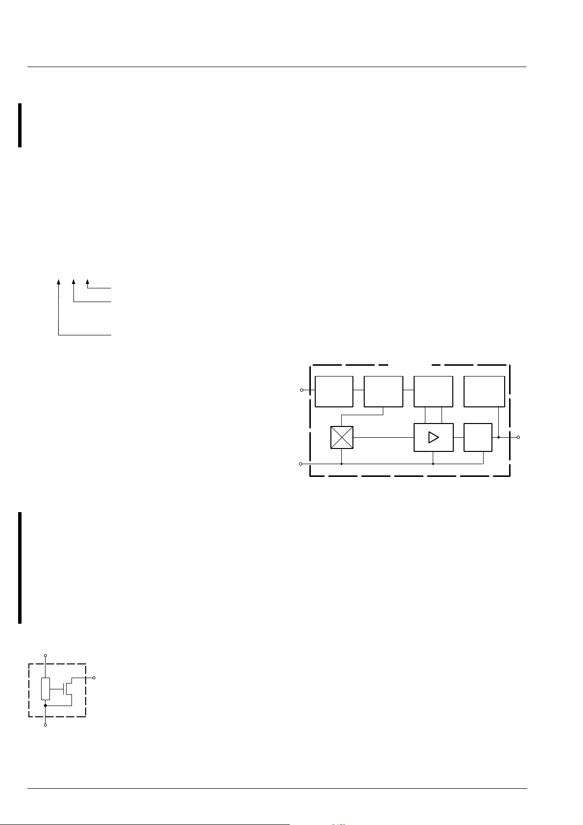
2. Functional Description
The HAL11x sensors are monolithic integrated circuits
which switch in response to magnetic fields. If a
magnetic field with flux lines perpendicular to the
sensitive area is applied to the sensor, the biased Hall
plate forces a Hall voltage proportional to this field. The
Hall voltage is compared with the actual threshold level
in the comparator. The temperature-dependent bias
increases the supply voltage of the Hall plates and
adjusts the switching points to the decreasing induction
of magnets at higher temperatures. If the magnetic field
exceeds the threshold levels, the open drain output
switches to the appropriate state. The built-in hysteresis
eliminates oscillation and provides switching behavior of
output without bouncing.
Shunt protection devices clamp voltage peaks at the
Output-pin and V
resistors. Reverse current is limited at the V
-pin together with external series
DD
-pin by an
DD
internal series resistor up to –15 V . No external reverse
protection diode is needed at the V
-pin for reverse
DD
voltages ranging from 0 V to –15 V.
HAL11x
Reverse
V
DD
ND
1
2
Voltage &
Overvoltage
Protection
Temperature
Dependent
Bias
Hall Plate
Hysteresis
Control
Comparator
Short Circuit &
Overvoltage
Protection
Output
OUT
3
1.6. Solderability
all packages: according to IEC68-2-58
During soldering reflow processing and manual
reworking, a component body temperature of 260 °C
should not be exceeded.
Components stored in the original packaging should
provide a shelf life of at least 12 months, starting from the
date code printed on the labels, even in environments as
extreme as 40 °C and 90% relative humidity.
V
DD
1
OUT
3
2
GND
Fig. 1–1: Pin configuration
Fig. 2–1: HAL11x block diagram
4 Micronas
Page 5
3. Specifications
3.1. Outline Dimensions
0.125
0.7
±0.2
4
min.
0.25
1.53
±0.05
123
±0.1
4.55
x1 x2
1.7
2
0.4
1.5
3.0
HAL11x
±0.1
0.48
0.55
0.42
4.06
x2x1
123
1.271.27
(2.54)
±0.2
0.75
sensitive area
y
±0.1
3.05
±0.2
3.1
14.0
min.
±0.05
1.5
0.3
sensitive area
y
±0.1
2.6
top view
0.40.4
0.36
branded side
±0.04
SPGS7001-7-A3/2E
0.06
Fig. 3–1:
Plastic Small Outline Transistor Package
(SOT-89A)
Weight approximately 0.04 g
Dimensions in mm
Note: The SOT-89A package will be discontinued in
2000 and be replaced by the SOT-89B package.
±0.1
4.55
x1 x2
0.125
0.3
±0.2
4
min.
0.25
±0.05
1.15
1.7
2
123
0.40.4
0.4
1.5
3.0
y
2.55
sensitive area
±0.1
top view
branded side
45°
SPGS7002-7-A/2E
0.8
Fig. 3–3:
Plastic Transistor Single Outline Package
(TO-92UA)
Weight approximately 0.12 g
Dimensions in mm
Note: For all package diagrams, a mechanical tolerance
of ±50 µm applies to all dimensions where no tolerance
is explicitly given.
3.2. Dimensions of Sensitive Area
0.4 mm x 0.2 mm
3.3. Positions of Sensitive Areas
SOT-89A SOT-89B TO-92UA
|x2 – x1| / 2 < 0.2 mm
y = 0.98 mm
± 0.2 mm
y = 0.95 mm
± 0.2 mm
y = 1.0 mm
± 0.2 mm
branded side
SPGS0022-3-A3/2E
Fig. 3–2:
Plastic Small Outline Transistor Package
(SOT-89B)
Weight approximately 0.035 g
Dimensions in mm
0.06
±0.04
5Micronas
Page 6
HAL11x
3.4. Absolute Maximum Ratings
Symbol Parameter Pin No. Min. Max. Unit
V
DD
–V
P
–I
DD
I
DDZ, IOZ
V
O
I
O
I
Omax
T
S
T
J
1)
as long as TJmax is not exceeded
2)
with a 220 Ω series resistor at pin 1
3)
t<2 ms
Supply Voltage 1 –15 28
Test Voltage for Supply 1 –24
Reverse Supply Current 1 – 50
Current through Protection Devices 1 or 3 –200
Output Voltage 3 –0.3 28
Continuous Output On Current 3 – 30
Peak Output On Current 3 – 250
Storage Temperature Range –65 150 °C
Junction Temperature Range –40 150 °C
2)
3)
1)
– V
1)
3)
200
1)
1)
3)
V
mA
mA
V
mA
mA
Stresses beyond those listed in the “Absolute Maximum Ratings” may cause permanent damage to the device. This
is a stress rating only . Functional operation of the device at these or any other conditions beyond those indicated in the
“Recommended Operating Conditions/Characteristics” of this specification is not implied. Exposure to absolute maximum ratings conditions for extended periods may affect device reliability.
3.5. Recommended Operating Conditions
Symbol Parameter Pin No. Min. Max. Unit
V
DD
I
O
V
O
Supply Voltage 1 4.5 24 V
Continuous Output On Current 3 0 20 mA
Output Voltage
3 0 24 V
(output switched off)
R
V
1)
see Fig. 5–1 on page 14
Series Resistor
1)
1 270 Ω
6 Micronas
Page 7

HAL11x
3.6. Electrical Characteristics at TJ = –40 °C to +140 °C , VDD = 4.5 V to 24 V , as not otherwise specified in Conditions
Typical Characteristics for TJ = 25 °C and VDD = 12 V
Symbol Parameter Pin No. Min. Typ. Max. Unit Conditions
I
DD
I
DD
V
OL
V
OL
I
OH
I
OH
t
en(O)
t
r
t
f
R
thJSB
case
SOT-89A
SOT-89B
Supply Current 1 6 8.2 11 mA
Supply Current over
1 3.9 8.2 12 mA
TJ= 25 °C
T emperature Range
Output Voltage over
3 – 120 400 mV IOL = 12.5 mA
T emperature Range
Output Voltage over
3 – 190 500 mV IOL = 20 mA
T emperature Range
Output Leakage Current 3 – 0.06 1 µA B < B
Output Leakage Current over
3 – – 10 µA B < B
Temperature Range
Enable Time of Output after
Setting of V
DD
1 – 6 10 µs VDD = 12 V
,
off
T
= 25 °C, VOH = 0 to 24 V
J
,
off
V
= 0 to 24V
OH
B > B
+ 2 mT or
ON
B < B
OFF
– 2 mT
Output Rise Time 3 – 0.08 0.4 µs VDD = 12 V, RL = 820 Ohm,
C
= 20 pF
L
Output Fall Time 3 – 0.06 0.4 µs VDD = 12 V, RL = 820 Ohm,
C
= 20 pF
L
Thermal Resistance Junction
to Substrate Backside
– – 150 200 K/W Fiberglass Substrate
30 mm x 10 mm x 1.5mm,
pad size see Fig. 3–4
R
thJA
case
Thermal Resistance Junction
to Soldering Point
TO-92UA
5.0
2.0
2.0
1.0
Fig. 3–4: Recommended pad size SOT-89x
Dimensions in mm
– – 150 200 K/W
7Micronas
Page 8

HAL11x
3.7. Magnetic Characteristics at TJ = –40 °C to +140 °C, VDD = 4.5 V to 24 V,
Typical Characteristics for VDD = 12 V
Magnetic flux density values of switching points.
Positive flux density values refer to the magnetic south pole at the branded side of the package.
Sensor Parameter On point B
Switching type T
HAL114 –40 °C 7.5 21.5 36 4.3 17.4 33.2 2.8 4.1 5 mT
unipolar 25 °C 7 21.1 34 4 17.1 31.2 2.8 4 4.5 mT
HAL115 –40 °C –10.7 1.4 12.5 –12.5 –1.4 10.7 1.8 2.8 7 mT
bipolar 25 °C –10.7 1.2 12.5 –12.5 –1.2 10.7 1.8 2.4 7 mT
J
140 °C 6.1 19.4 31.3 3.6 16.1 28.8 2.2 3.3 4 mT
140 °C –10.7 0.9 12.5 –12.5 –0.9 10.7 1 1.8 7 mT
Min. Typ. Max. Min. Typ. Max. Min. Typ. Max.
ON
Off point B
OFF
Hysteresis B
HYS
Unit
Note: For detailed descriptions of the individual types, see pages 10 and following.
The magnetic limits given above refer to parts in the original packaging. Mechanical stress on the hall sensitive areas
on the chip surface may generate an additional magnetic offset, which can slightly change the magnetic switching
points. This behavior is a physical phenomenon and not a malfunction of the sensor. Mechanical stress on the hall plates
can be caused, for example, by overmoulding the plastic package or by wide range temperature changes like soldering
or operating the parts at extreme temperatures.
Please use a sensor of the HAL5xx family if higher robustness against mechanical stress is required.
mA
15
T
10
I
DD
5
0
–5
–10
–15
–15 –10 –5 0 5 1015202530
A
T
A
T
A
Fig. 3–5: Typical supply current
versus supply voltage
HAL11x
= –40 °C
= 25 °C
= 140 °C
V
DD
mA
12
10
I
DD
8
6
4
2
0
V
0123456
T
= –40 °C
A
T
= 25 °C
A
T
= 140 °C
A
V
DD
HAL11x
V
Fig. 3–6: Typical supply current
versus supply voltage
8 Micronas
Page 9

HAL11x
mA
12
10
I
DD
V
= 4.5 V
DD
8
6
4
2
0
VDD = 24 V
–50 0 50 100 150
Fig. 3–7: Typical supply current
versus temperature
HAL11x
T
A
°C
mV
500
V
400
OL
300
I
= 20 mA
O
200
100
0
–50 0 50 100 150
VDD = 12 V
IO = 12.5 mA
T
A
Fig. 3–9: Typical output low voltage
versus temperature
HAL11x
°C
mV
500
IO = 12.5 mA
V
400
OL
300
T
= 140 °C
A
200
T
= 25 °C
A
100
T
= –40 °C
A
0
0 5 10 15 20 25 30
V
DD
Fig. 3–8: Typical output low voltage
versus supply voltage
HAL11x
µA
2
10
1
10
I
OH
0
10
–1
10
–2
10
–3
10
–4
10
V
–50 0 50 100 150
HAL11x
VOH = 24 V
VDD = 5 V
T
A
°C
Fig. 3–10: T ypical output leakage current
versus temperature
9Micronas
Page 10

HAL114
4. Type Description
4.1. HAL114
The HAL114 is a unipolar switching sensor (see
Fig. 4–1).
The output turns low with the magnetic south pole on the
branded side of the package and turns high if the magnetic field is removed. The sensor does not respond to
the magnetic north pole on the branded side.
For correct functioning in the application, the sensor requires only the magnetic south pole on the branded side
of the package.
Magnetic Features:
– switching type: unipolar
– typical B
– typical B
: 21.1 mT at room temperature
ON
: 17.1 mT at room temperature
OFF
– operates with static magnetic fields and dynamic mag-
netic fields up to 20 kHz
Applications
The HAL114 is the optimal sensor for applications with
one magnetic polarity such as:
– solid state switches,
– contactless solution to replace micro switches,
– position and end-point detection, and
– rotating speed measurement.
Output Voltage
V
O
B
HYS
V
OL
0B
OFF
B
ON
B
Fig. 4–1: Definition of magnetic switching points for
the HAL114
Magnetic Characteristics at TJ = –40 °C to +140 °C, VDD = 4.5 V to 24 V,
Typical Characteristics for VDD = 12 V
Magnetic flux density values of switching points.
Positive flux density values refer to the magnetic south pole at the branded side of the package.
Parameter On point B
T
J
–40 °C 7.5 21.5 36 4.3 17.4 33.2 2.8 4.1 5 mT
25 °C 7 21.1 34 4 17.1 31.2 2.8 4 4.5 mT
100 °C 6.3 19.9 31.5 3.6 16.4 28.9 2.6 3.5 4 mT
140 °C 6.1 19.4 31.3 3.6 16.1 28.8 2.2 3.3 4 mT
Min. Typ. Max. Min. Typ. Max. Min. Typ. Max.
ON
The hysteresis is the difference between the switching points B
Off point B
HYS
OFF
= BON – B
OFF
Hysteresis B
HYS
Unit
The magnetic limits given above refer to parts in the original packaging. Mechanical stress on the hall sensitive areas
on the chip surface may generate an additional magnetic offset, which can slightly change the magnetic switching
points. This behavior is a physical phenomenon and not a malfunction of the sensor. Mechanical stress on the hall plates
can be caused, for example, by overmoulding the plastic package or by wide range temperature changes like soldering
or operating the parts at extreme temperatures.
Please use a sensor of the HAL 5xx family if a robustness against mechanical stress is required.
10 Micronas
Page 11

HAL114
mT
30
B
ON
B
OFF
25
20
15
T
= –40 °C
10
A
T
= 25 °C
A
T
= 140 °C
A
5
0
0 5 10 15 20 25 30
V
DD
Fig. 4–2: T ypical magnetic switching
points versus supply voltage
HAL114
mT
30
B
ON
25
B
OFF
B
ON
V
DD
HAL114
= 12 V
20
B
15
OFF
10
5
0
V
–50 0 50 100 150
T
A
°C
Fig. 4–4: Typical magnetic switching
points versus temperature
mT
30
B
ON
B
OFF
25
20
15
T
= –40 °C
10
A
T
= 25 °C
A
T
= 140 °C
A
5
0
3456
V
DD
Fig. 4–3: Typical magnetic switching
points versus supply voltage
HAL114
V
11Micronas
Page 12

HAL115
4.2. HAL115
The HAL1 15 is a bipolar switching sensor (see Fig. 4–5).
The output turns low with the magnetic south pole on the
branded side of the package and turns high with the
magnetic north pole on the branded side. The output
state is not defined for all sensors if the magnetic field is
removed again. Some sensors will change the output
state and some sensors will not.
For correct functioning in the application, the sensor requires both magnetic polarities (north and south) on the
branded side of the package.
Magnetic Features:
– switching type: bipolar
– high sensitivity
– typical B
– typical B
: 1.2 mT at room temperature
ON
: –1.2 mT at room temperature
OFF
– operates with static magnetic fields and dynamic mag-
netic fields up to 20 kHz
Applications
The HAL 115 is the optimal sensor for all applications
with alternating magnetic signals at the sensor position
such as:
– rotating speed measurement,
– commutation of brushless DC-motors and cooling
fans.
Output Voltage
V
O
B
HYS
V
OL
0B
OFF
B
ON
B
Fig. 4–5:Definition of magnetic switching points for the
HAL115
Magnetic Characteristics at TJ = –40 °C to +140 °C, VDD = 4.5 V to 24 V,
Typical Characteristics for VDD = 12 V
Magnetic flux density values of switching points.
Positive flux density values refer to the magnetic south pole at the branded side of the package.
Parameter On point B
T
J
–40 °C –10.7 1.4 12.5 –12.5 –1.4 10.7 1.8 2.8 7 mT
25 °C –10.7 1.2 12.5 –12.5 –1.2 10.7 1.8 2.4 7 mT
100 °C –10.7 1 12.5 –12.5 –1 10.7 1.5 2 7 mT
140 °C –10.7 0.9 12.5 –12.5 –0.9 10.7 1 1.8 7 mT
Min. Typ. Max. Min. Typ. Max. Min. Typ. Max.
ON
The hysteresis is the difference between the switching points B
Off point B
HYS
OFF
= BON – B
OFF
Hysteresis B
HYS
Unit
The magnetic limits given above refer to parts in the original packaging. Mechanical stress on the hall sensitive areas
on the chip surface may generate an additional magnetic offset, which can slightly change the magnetic switching
points. This behavior is a physical phenomenon and not a malfunction of the sensor. Mechanical stress on the hall plates
can be caused, for example, by overmoulding the plastic package or by wide range temperature changes like soldering
or operating the parts at extreme temperatures.
Please use a sensor of the HAL5xx family if higher robustness against mechanical stress is required.
12 Micronas
Page 13

HAL115
mT
6
B
ON,
4
B
OFF
2
0
–2
–4
–6
–50 0 50 100 150
B
B
ON
OFF
HAL115
VDD = 12 V
T
A
Fig. 4–6:Typical magnetic switching
points versus ambient temperature
°C
13Micronas
Page 14

HAL11x
5. Application Notes
5.1. Application Circuit
The HAL1 1x sensors can operate without external components. For applications with disturbances on the supply line or radiated disturbances, a series resistor and a
capacitor are recommended (see Fig. 5–1).
The series resistor and the capacitor should be placed
as closely as possible to the sensor.
R
V
220 Ω
R
1V
DD
V
DD
4.7 nF
2
GND
OUT
3
L
Fig. 5–1: Recommended application circuit
5.2. Ambient Temperature
Due to the internal power dissipation, the temperature
on the silicon chip (junction temperature T
) is higher
J
than the temperature outside the package (ambient temperature T
).
A
TJ = TA + ∆T
At static conditions, the following equation is valid:
∆T = I
* VDD * R
DD
th
For typical values, use the typical parameters. For worst
case calculation, use the max. parameters for I
DD
and
Rth, and the max. value for VDD from the application.
For all sensors, the junction temperature range T
specified. The maximum ambient temperature T
is
J
Amax
can be calculated as:
T
Amax
= T
Jmax
– ∆T
5.3. Extended Operating Conditions
All sensors fulfill the electrical and magnetic characteristics when operated within the Recommended Operating
Conditions (see page 6).
V
DD
L
2
1
HAL115
2
3.3 k R
3
L
1
1
R
2
3.3 k
2.2 µ/50 V 2.2 µ
C
1
Fig. 5–2: Recommended application circuit
for DC fans
/50 V
C
2
Please use the sensors of the HAL 5xx family if lower operation voltage, lower current consumption or tighter
magnetic specifications required.
5.4. Start-up Behavior
The sensors have an initialization time (enable time
t
) after applying the supply voltage. This parameter
en(O)
t
is specified in the Electrical Characteristics (see
en(O)
page 7).
During the initialization time, the output state is not de-
fined and can toggle. After t
, the output will be low
en(O)
if the applied magnetic field B is above BON or high if B
is below B
For magnetic fields between B
OFF
.
and BON, the output
OFF
state of the HAL sensor after applying VDD will be either
low or high. In order to achieve a well-defined output
state, the applied magnetic field must be above B
respectively, below B
OFFmin
.
ONmax
,
14 Micronas
Page 15

HAL11x
15Micronas
Page 16

HAL11x
6. Data Sheet History
1. Final data sheet: “HAL114 Unipolar Hall Switch IC”,
June 10, 1998, 6251-456-1DS. First release of the final
data sheet.
2. Final data sheet: “HAL115 Hall Effect Sensor IC”,
May 7, 1997, 6251-414-1DS. First release of the final
data sheet.
3. Final data sheet: “HAL114, HAL115 Hall Effect Sensor Family, Dec. 20, 1999, 6251-456-2DS. Second release of the final data sheet. Major changes:
– additional package SOT-89B
– temperature range “A” replaced by “K” for HAL114
– additional temperature range “K” for HAL115
– outline dimensions for SOT-89A and TO-92UA
changed
– supply voltage range changed for HAL115
Micronas GmbH
Hans-Bunte-Strasse 19
D-79108 Freiburg (Germany)
P.O. Box 840
D-79008 Freiburg (Germany)
Tel. +49-761-517-0
Fax +49-761-517-2174
E-mail: docservice@micronas.com
Internet: www.micronas.com
Printed in Germany
by Systemdruck+Verlags-GmbH, Freiburg (12/1999)
Order No. 6251-456-2DS
All information and data contained in this data sheet are without any
commitment, are not to be considered as an offer for conclusion of a
contract, nor shall they be construed as to create any liability . Any new
issue of this data sheet invalidates previous issues. Product availability
and delivery are exclusively subject to our respective order confirmation form; the same applies to orders based on development samples
delivered. By this publication, Micronas GmbH does not assume responsibility for patent infringements or other rights of third parties
which may result from its use.
Further, Micronas GmbH reserves the right to revise this publication
and to make changes to its content, at any time, without obligation to
notify any person or entity of such revisions or changes.
No part of this publication may be reproduced, photocopied, stored on
a retrieval system, or transmitted without the express written consent
of Micronas GmbH.
16 Micronas
Page 17

HAL 11x, HAL 5xx, HAL 62x
Data Sheet Supplement
Subject:
Data Sheet Concerned:
Improvement of SOT-89B P ackage
HAL 114, 115, 6251-456-2DS, Dec. 20, 1999
HAL 50x, 51x, 6251-485-1DS, Feb. 16, 1999
HAL 55x, 56x, 6251-425-1DS, April 6, 1999
HAL 621, 629, 6251-504-1DS, Feb. 3, 2000
Supplement:
Edition:
Changes:
– position tolerance of the sensitive area reduced
– tolerances of the outline dimensions reduced
– thickness of the leadframe changed to 0.15 mm (old 0.125 mm)
– SOT-89A will be discontinued in December 2000
sensitive area
∅0.2
y
0.15
0.3
4.55
1.7
2
No. 1/ 6251-531-1DSS
July 4, 2000
±0.2
4
min.
0.25
1.15
SPGS0022-5-A3/2E
123
0.4
1.5
3.0
branded side
2.55
top view
0.40.4
±0.04
0.06
Position of sensitive area
HAL 114, 115
HAL 55x, HAL 56x
HAL 50x, 51x
HAL 621, 629
x center of the package center of the package
y 0.95 mm nomi nal 0.85 mm nominal
Note: A mechanical tolerance of ±0.05 mm applies to all dimensions where no tolerance is e xplicitly given.
Position tolerance of the sensitive area is defined in the package diagram.
Micronas page 1 of 1
 Loading...