

Page 1
HI-SINCERITY
MICROELECTRONICS CORP.
Spec. No. : HE6108
Issued Date : 1997.09.05
Revised Date : 2001.08.13
Page No. : 1/3
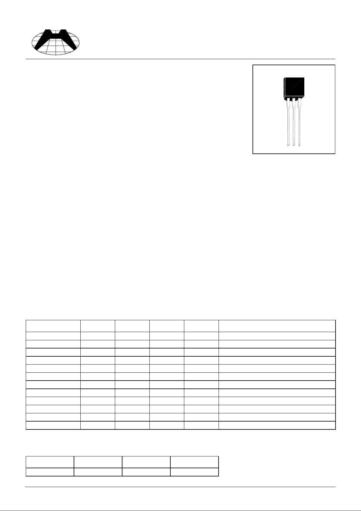
HA8550
PNP EPITAXIAL PLANAR TRANSIST OR
Description
The HA8550 is designed for use in 2W output amplifier of portable radios in
class B push-pull operation.
Features
High total power dissipation (PT: 2W, TC=25°C)
•
High collector current (IC: 1.5A)
•
Complementary to HA8050
•
Absolute Maximum Ratings
Maximum Temperatures
•
Storage Temperature....................................................................................................... -55 ~ +150 °C
Junction Temperature................................................................................................ +150 °C Maximum
Maximum Power Dissipation
•
Total Power Dissipation (Ta=25°C)................................................................................................... 1 W
Total Power Dissipation (Tc=25°C)................................................................................................... 2 W
Maximum Voltages and Currents (Ta=25°C)
•
VCBO Collector to Base Voltage.................................................................................................... -40 V
VCEO Collector to Emitter Voltage ................................................................................................. -25 V
VEBO Emitter to Base Voltage......................................................................................................... -6 V
IC Collector Current ..................................................................................................................... -1.5 A
IB Base Current ............................................................................................................................ -0.5 A
(Ta=25°C)
Characteristics
Symbol Min. Typ. Max. Unit Test Conditions
BVCBO -40 - - V IC=-100uA
BVCEO -25 - - V IC=-2mA
BVEBO -6 - - V IE=-100uA
ICBO - - -100 nA VCB=-35V
IEBO - - -100 nA VEB=-6V
*VCE(sat) - - -0.5 V IC=-0.8A, IB=-80mA
*VBE(sat) - - -1.2 V IC=-0.8A, IB=-80mA
VBE(on) - - -1 V VCE=-1V, IC=-10mA
*hFE1 45 - - VCE=-1V, IC=-5mA
*hFE2 85 - 500 VCE=-1V, IC=-100mA
*hFE3 40 - - VCE=-1V, IC=-800mA
fT 100 - - MHz VCE=-10V, IC=-50mA, f=100MHZ
*Pulse Test : Pulse Width ≤380us, Duty Cycle≤2%
Classification on hFE2
Rank C D E
Range 120-200 160-320 250-500
HA8550 HSMC Product Specification
Page 2
HI-SINCERITY
MICROELECTRONICS CORP.
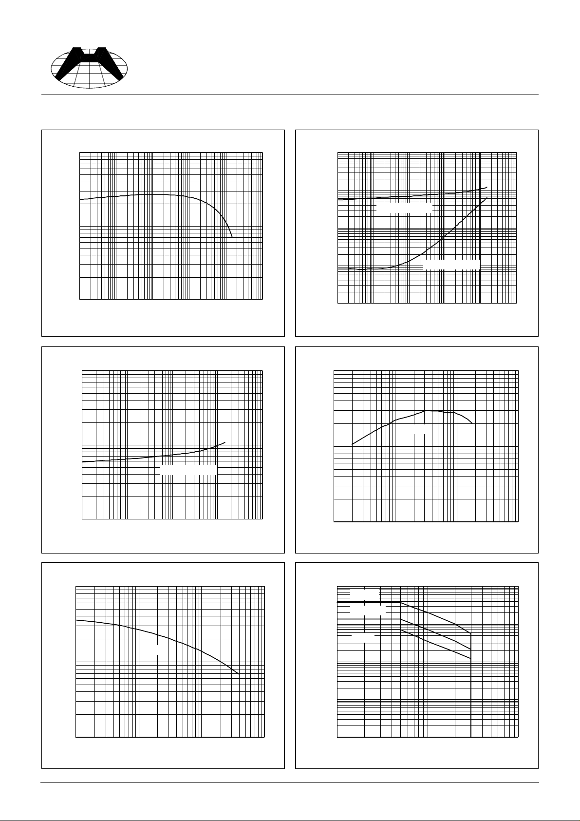
Characteristics Curve
Spec. No. : HE6108
Issued Date : 1997.09.05
Revised Date : 2001.08.13
Page No. : 2/3
1000
100
hFE
10
0.1 1 10 100 1000 10000
10000
Current Gain & Collector Current
Collector Curremt-IC (mA)
On Vol t age & Collector Cur rent
10000
1000
Satu r ation Voltage (mV)
1000
Saturation Volt age & Coll ector Cu rren t
BE(sat)
V
100
10
1
0.1 1 10 100 1000 10000
Collector Curren t-IC (mA)
@ IC=10I
B
CE(sat)
V
@ IC=10I
B
Cut o ff Fr equency & Collect or Current
1000
BE(on)
V
On Voltage (mV)
100
1 10 100 1000 10000
Collector Curren t-IC (mA)
100
10
Capac itanc e (pF)
Capcitance & Reverse-Biased Voltage
Cob
@ VCE=1V
VCE=10V
100
Cutoff Frequency (MHz)
10
1 10 100 1000
10000
1000
(mA)
C
100
Collector Curren t-I
PT=1ms
PT=100ms
PT=1s
10
Collector Curren t-IC (mA)
Safe Operating Area
1
0.1 1 10 100
Reverse-Biased Vol t ag e ( V)
1
1 10 100
Forwar d Vol tage-VCE (V)
HA8550 HSMC Product Specification
Page 3

HI-SINCERITY
g
MICROELECTRONICS CORP.
TO-92 Dimension
A
Spec. No. : HE6108
Issued Date : 1997.09.05
Revised Date : 2001.08.13
Page No. : 3/3
α
2
Marking :
C
B
31
2
α
3
HSMC Logo
Part Number
Date Code
HSMC Logo
D
Part Number
H
α
I
1
G
Style : Pin 1.Emitter 2.Base 3.Collec tor
Product Series
Rank
Laser Mark
Product Series
Ink Mark
E
F
DIM
A 0.1704 0.1902 4.33 4.83 G 0.0142 0.0220 0.36 0.56
B 0.1704 0.1902 4.33 4.83 H - *0.1000 - *2.54
C 0.5000 - 12.70 - I - *0.0500 - *1.27
D 0.0142 0.0220 0.36 0.56
E - *0.0500 - *1.27
F 0.1323 0.1480 3.36 3.76
Notes :
Material :
• Lead : 42 Alloy ; solder plating
• Mold Compound : Epoxy resin family, flammability solid burning class:UL94V-0
1.Dimension and tolerance based on our Spec. dated Apr. 25,1996.
2.Controlling dimension : millimeters.
3.Maximum lead thickness includes lead finish thickness, and minimum lead thickness is the minimum thickness of base material.
4.If there is any question with packing specification or packing method, please contact your l ocal HSMC sales office.
Inches Millimeters Inches Millimeters
Min. Max. Min. Max.
3-Lead TO-92 Plastic Package
HSMC Packa
e Code : A
DIM
1
α
2
α
3
α
Min. Max. Min. Max.
-
-
-
*5
*2
*2
°
°
°
-
-
-
*:Typical
*5
°
*2
°
*2
°
Important Notice:
• All rights are reserved. Reproduction in whole or in part is prohibited without the prior written approval of HSMC.
• HSMC reserves the right to make changes to its products without notice.
•
HSMC semiconductor products are not warranted to be suitable for use in Life-Support Applications, or systems.
• HSMC assumes no liability for any consequence of customer product design, infringement of patents, or appl ication assistance.
Head Office And Factory :
•
Head Office
Tel : 886-2-25212056 Fax : 886-2-25632712, 25368454
•
Factory 1 :
Tel : 886-3-5983621~5 Fax : 886-3-5982931
HA8550 HSMC Product Specification
(Hi-Sincerity Microelectronics Corp.) : 10F.,No. 61, Sec. 2, Chung-Shan N. Rd. Taipei Taiwan R.O.C.
No. 38, Kuang Fu S. Rd., Fu-Kou Hsin-Chu Industrial Park Hsin-Chu Taiwan. R.O.C
 Loading...