

Page 1
HA17747/P
Dual Operational Amplifier
Description
The HA17747/P is a dual internal phase compensation high-performance operational amplifier, that is
appropriate for use in a wide range of applications in the test and control fields.
Features
• High voltage gain : 106 dB (Typ)
• Wide output amplitude : ±13 V (Typ) (at RL ≥ 2 kΩ)
• Shorted output protection
• Adjustable offset voltage
• Internal phase compensation
Ordering Information
Type No. Application Package
HA17747P Industrial use DP-14
HA17747 Commercial use
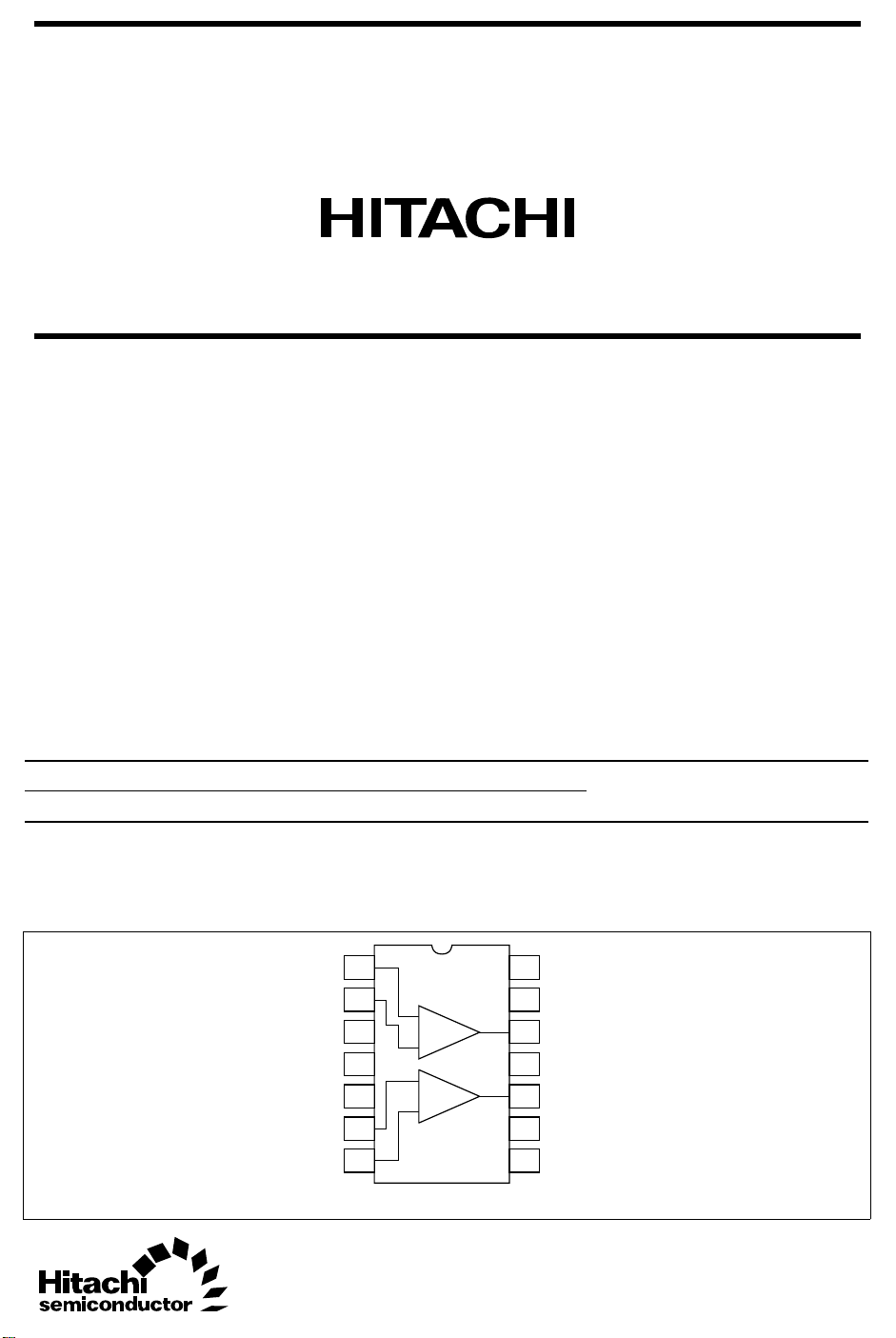
Pin Arrangement
Offset
Vin(−)1
Vin(+)1
Offset
Null 1
V
Offset
Null 2
Vin(+)2
Vin(−)2
1
2
3
4
EE
5
6
7
−
1
+
+
2
−
(Top view)
14
13
12
11
10
9
8
Null 1
V
1
CC
Output 1
NC
Output 2
V
2
CC
Offset
Null 2
Page 2
HA17747/P
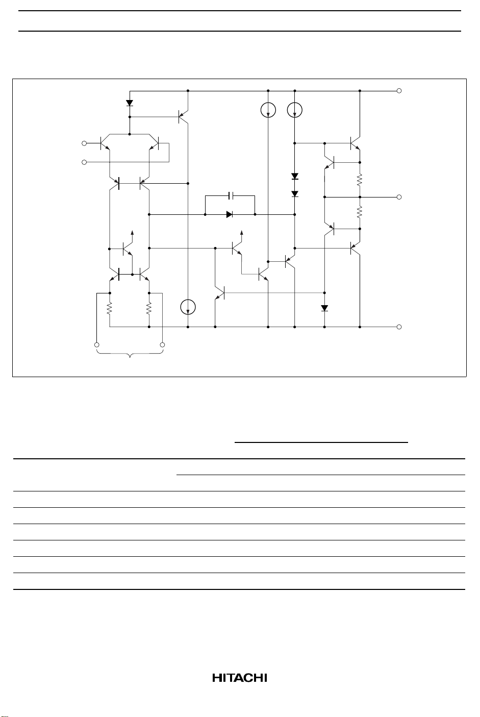
Circuit Structure
Vin(+)
Vin(−)
V
CC
Vout
To V
CC
To V
CC
V
EE
Offset Null
Absolute Maximum Ratings (Ta = 25°C)
Ratings
Item Symbol HA17747P HA17747 Unit
Power-supply voltage V
CC
V
EE
Input voltage Vin ±15 *
Differential input voltage Vin(diff) ±30 ±30 V
Offset adjustment pin – VEE voltage V
Allowable power dissipation P
OFF
T
– V
Operating temperature Topr –20 to +75 –20 to +75 °C
Storage temperature Tstg –55 to +125 –55 to +125 °C
Notes: 1. When the power-supply voltage is less than ±15 V, the input voltage must fall within the power-
supply voltage range.
2. These are the allowable values up to Ta = 45°C. Above that temperature, derate by 8.3 mW/°C.
+18 +18 V
–18 –18 V
1
±0.5 ±0.5 V
EE
2
670 *
±15 *
670 *
1
2
V
mW
2
Page 3

HA17747/P
Electrical Characteristics
Electrical Characteristics-1 (VCC = –VEE = 15 V, Ta = 25°C)
Item Symbol Min Typ Max Unit Test Condition
Input offset voltage V
Input offset current I
Input bias current I
Voltage gain A
Supply current I
IO
IO
IB
VD
CC
Power dissipation Pd — 50 85 mW (per channel rating)
Input resistance Rin 0.3 2.0 — MΩ
Input capacitance Cin — 1.4 — pF
Output resistance Rout — 75 — Ω
Slew rate SR — 1.0 — V/µsRL ≥ 2 kΩ
Rise time t
r
Overshoot Vover — 5.0 — % RL = 2 kΩ, CL = 100 pF
Input offset voltage adjustment range ∆V
Output shorted current I
IO(adj)
OS
Channel separation CS — 120 — dB
— 1.0 6.0 mV RS ≤ 10 kΩ
— 20 200 nA
— 80 500 nA
88 106 — dB RL ≥ 2 kΩ, Vout = ±10 V
— 1.7 2.8 mA No load
— 0.3 — µs Vin = –20 mV,
— ±15 — mV
—25—mA
Electrical Characteristics-2 (VCC = –VEE = 15 V, Ta = –20 to +75°C)
Item Symbol Min Typ Max Unit Test Condition
Input offset voltage V
Input offset current I
Input bias current I
IO
IO
IB
Power-supply rejection ratio ∆VIO/∆VCC— 30 150 µV/V RS ≤ 10 kΩ
∆VIO/∆VEE— 30 150 µV/V RS ≤ 10 kΩ
Voltage gain A
VD
Common-mode rejection ratio CMR 70 90 — dB RS ≤ 10 kΩ
Common-mode input voltage range V
Maximum output V
CM
OP-P
voltage amplitude ±10 ±13 — V RL ≥ 2 kΩ
Supply current I
CC
Power dissipation Pd — 65 110 mW (per channel rating)
— 1.0 9.0 mV RS ≤ 10 kΩ
— 20 400 nA
— 80 1,100 nA
80——dBR
≥ 2 kΩ, Vout = ±10 V
L
±12 ±13 — V
±12 ±14 — V RL ≥ 10 kΩ
— 2.1 3.7 mA No load
3
Page 4

HA17747/P
Package Dimensions
1
19.20
20.32 Max
1.30
Unit: mm
814
6.30
7.40 Max
7
2.54 ± 0.25
2.39 Max
0.48 ± 0.10
2.54 Min 5.06 Max
0.51 Min
Hitachi Code
JEDEC
EIAJ
Mass
7.62
+ 0.10
0.25
– 0.05
0° – 15°
(reference value)
DP-14
Conforms
Conforms
0.97 g
4
Page 5

HA17747/P
Cautions
1. Hitachi neither warrants nor grants licenses of any rights of Hitachi’s or any third party’s patent,
copyright, trademark, or other intellectual property rights for information contained in this document.
Hitachi bears no responsibility for problems that may arise with third party’s rights, including
intellectual property rights, in connection with use of the information contained in this document.
2. Products and product specifications may be subject to change without notice. Confirm that you have
received the latest product standards or specifications before final design, purchase or use.
3. Hitachi makes every attempt to ensure that its products are of high quality and reliability. However,
contact Hitachi’s sales office before using the product in an application that demands especially high
quality and reliability or where its failure or malfunction may directly threaten human life or cause risk
of bodily injury, such as aerospace, aeronautics, nuclear power, combustion control, transportation,
traffic, safety equipment or medical equipment for life support.
4. Design your application so that the product is used within the ranges guaranteed by Hitachi particularly
for maximum rating, operating supply voltage range, heat radiation characteristics, installation
conditions and other characteristics. Hitachi bears no responsibility for failure or damage when used
beyond the guaranteed ranges. Even within the guaranteed ranges, consider normally foreseeable
failure rates or failure modes in semiconductor devices and employ systemic measures such as failsafes, so that the equipment incorporating Hitachi product does not cause bodily injury, fire or other
consequential damage due to operation of the Hitachi product.
5. This product is not designed to be radiation resistant.
6. No one is permitted to reproduce or duplicate, in any form, the whole or part of this document without
written approval from Hitachi.
7. Contact Hitachi’s sales office for any questions regarding this document or Hitachi semiconductor
products.
Hitachi, Ltd.
Semiconductor & Integrated Circuits.
Nippon Bldg., 2-6-2, Ohte-machi, Chiyoda-ku, Tokyo 100-0004, Japan
Tel: Tokyo (03) 3270-2111 Fax: (03) 3270-5109
URL NorthAmerica : http:semiconductor.hitachi.com/
For further information write to:
Hitachi Semiconductor
(America) Inc.
179 East Tasman Drive,
San Jose,CA 95134
Tel: <1> (408) 433-1990
Fax: <1>(408) 433-0223
Europe : http://www.hitachi-eu.com/hel/ecg
Asia (Singapore) : http://www.has.hitachi.com.sg/grp3/sicd/index.htm
Asia (Taiwan) : http://www.hitachi.com.tw/E/Product/SICD_Frame.htm
Asia (HongKong) : http://www.hitachi.com.hk/eng/bo/grp3/index.htm
Japan : http://www.hitachi.co.jp/Sicd/indx.htm
Hitachi Europe GmbH
Electronic components Group
Dornacher Straβe 3
D-85622 Feldkirchen, Munich
Germany
Tel: <49> (89) 9 9180-0
Fax: <49> (89) 9 29 30 00
Hitachi Europe Ltd.
Electronic Components Group.
Whitebrook Park
Lower Cookham Road
Maidenhead
Berkshire SL6 8YA, United Kingdom
Tel: <44> (1628) 585000
Fax: <44> (1628) 778322
Hitachi Asia Pte. Ltd.
16 Collyer Quay #20-00
Hitachi Tower
Singapore 049318
Tel: 535-2100
Fax: 535-1533
Hitachi Asia Ltd.
Taipei Branch Office
3F, Hung Kuo Building. No.167,
Tun-Hwa North Road, Taipei (105)
Tel: <886> (2) 2718-3666
Fax: <886> (2) 2718-8180
Copyright ' Hitachi, Ltd., 1998. All rights reserved. Printed in Japan.
Hitachi Asia (Hong Kong) Ltd.
Group III (Electronic Components)
7/F., North Tower, World Finance Centre,
Harbour City, Canton Road, Tsim Sha Tsui,
Kowloon, Hong Kong
Tel: <852> (2) 735 9218
Fax: <852> (2) 730 0281
Telex: 40815 HITEC HX
5
 Loading...