

Page 1
HA17741/PS
General-Purpose Operational Amplifier
(Frequency Compensated)
Description
The HA17741/PS is an internal phase compensation high-performance operational amplifier, that is
appropriate for use in a wide range of applications in the test and control fields.
Features
• High voltage gain : 106 dB (Typ)
• Wide output amplitude : ±13 V (Typ) (at RL ≥ 2 kΩ)
• Shorted output protection
• Adjustable offset voltage
• Internal phase compensation
Ordering Information
Application Type No. Package
Industrial use HA17741PS DP-8
Commercial use HA17741
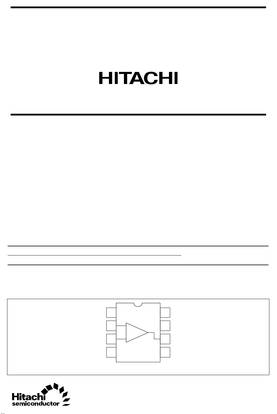
Pin Arrangement
Offset
Vin(−)
Vin(+)
Null
V
EE
1
2
3
4
−
+
(Top view)
8
7
6
5
NC
V
CC
Vout
Offset
Null
Page 2
HA17741/PS
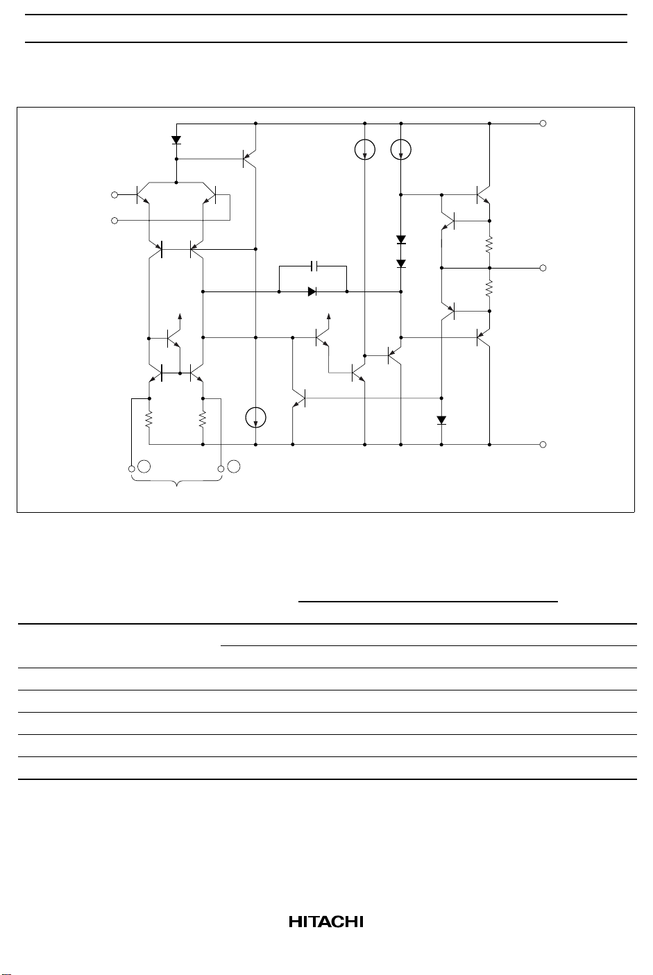
Circuit Structure
Vin(+)
Vin(−)
V
CC
Vout
To V
CC
1
Pin
5
Pin
To V
CC
V
EE
Offset Null
Absolute Maximum Ratings (Ta = 25°C)
Ratings
Item Symbol HA17741PS HA17741 Unit
Power-supply voltage V
CC
V
EE
Input voltage Vin ±15 ±15 V
Differential input voltage Vin(diff) ±30 ±30 V
Allowable power dissipation P
T
Operating temperature Topr –20 to +75 –20 to +75 °C
Storage temperature Tstg –55 to +125 –55 to +125 °C
Note: These are the allowable values up to Ta = 45°C. Derate by 8.3 mW/°C above that temperature.
+18 +18 V
–18 –18 V
670 * 670 * mW
2
Page 3
HA17741/PS
Electrical Characteristics
Electrical Characteristics-1 (VCC = –VEE = 15 V, Ta = 25°C)
Item Symbol Min Typ Max Unit Test Condition
Input offset voltage V
Input offset current I
Input bias current I
IO
IO
IB
Power-supply ∆VIO/∆VCC— 30 150 µV/V RS ≤ 10 kΩ
rejection ratio ∆VIO/∆VEE— 30 150 µV/V RS ≤ 10 kΩ
Voltage gain A
Common-mode
VD
CMR 70 90 — dB RS ≤ 10 kΩ
rejection ratio
Common-mode input
V
CM
voltage range
Maximum output V
OP-P
voltage amplitude ±10 ±13 — V RL ≥ 2 kΩ
Power dissipation Pd — 65 100 mW No load
Slew rate SR — 1.0 — V/µsRL ≥ 2 kΩ
Rise time t
r
Overshoot Vover — 5.0 — % CL = 100 pF
Input resistance Rin 0.3 1.0 — MΩ
— 1.0 6.0 mV RS ≤ 10 kΩ
— 18 200 nA
— 75 500 nA
86 106 — dB RL ≥ 2 kΩ, Vout = ±10 V
±12 ±13 — V RS ≤ 10 kΩ
±12 ±14 — V RL ≥ 10 kΩ
— 0.3 — µs Vin = 20 mV, RL = 2 kΩ,
Electrical Characteristics-2 (VCC = –VEE = 15 V, Ta = –20 to +75°C)
Item Symbol Min Typ Max Unit Test Condition
Input offset voltage V
Input offset current I
Input bias current I
Voltage gain A
Maximum output
voltage amplitude
IO
IO
IB
VD
V
OP-P
— — 9.0 mV RS ≤ 10 kΩ
— — 400 nA
— — 1,100 nA
80——dBR
±10——VR
≥ 2 kΩ, Vout = ±10 V
L
≥ 2 kΩ
L
3
Page 4
HA17741/PS
IC Operational Amplifier Application Examples
Multivibrator
A multivibrator is a square wave generator that uses an RC circuit charge/discharge operation to generate
the waveform. Multivibrators are widely used as the square wave source in such applications as power
supplies and electronic switches.
Multivibrators are classified into three types, astable multivibrators, which have no stable states,
monostable multivibrators, which have one stable state, and bistable multivibrators, which have two stable
states.
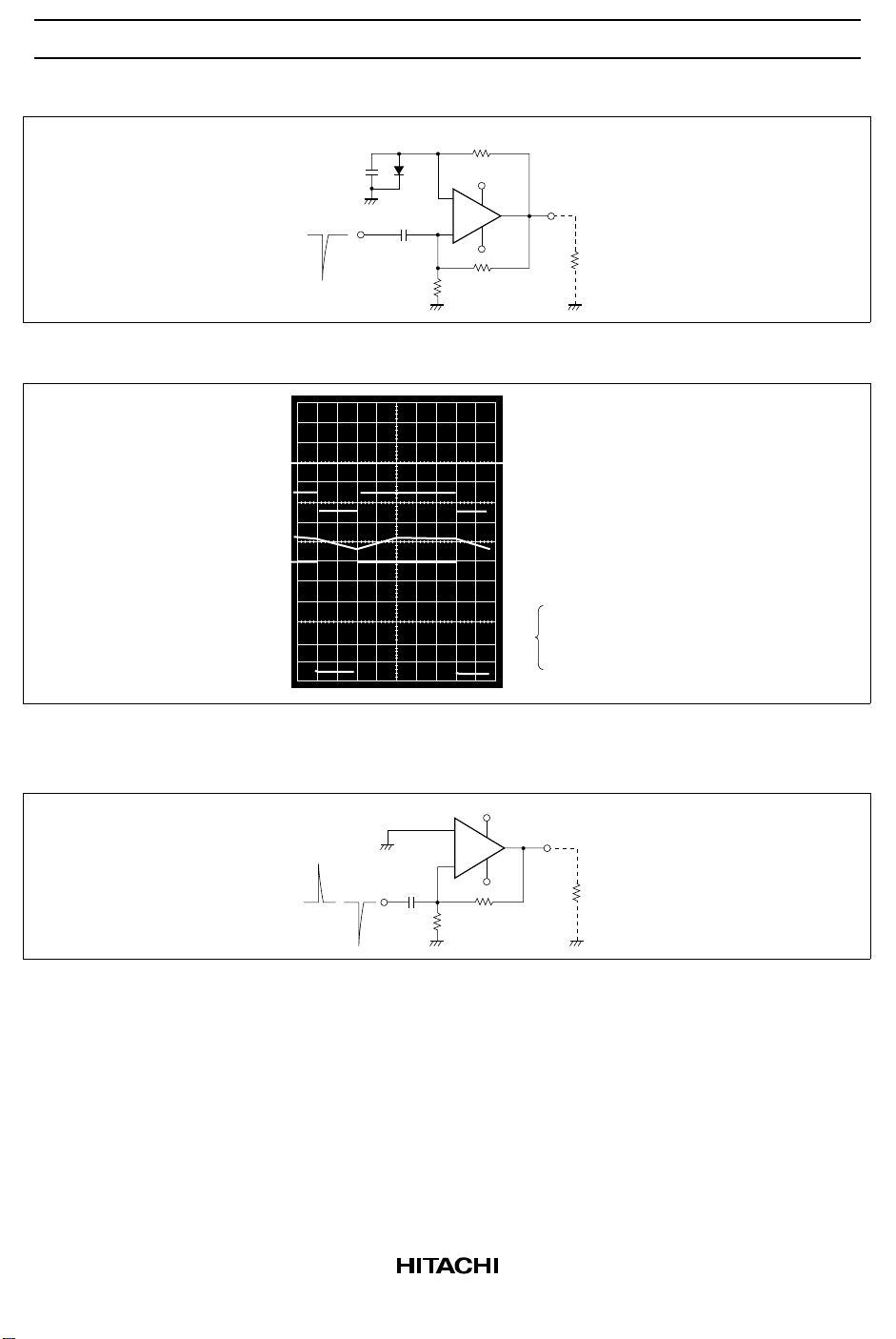
1. Astable Multivibrator
R
3
V
Vin(−)
−
Vin(+)
C
1
+
CC
Vout
R
V
EE
1
R
L
R
2
Figure 1 Astable Multivibrator Operating Circuit
Vin(+) 0
Vin(−) 0
Vout 0
Vertical:
Horizontal:
Circuit constants
R
R
R
V
5 V/div
2 ms/div
= 8 kΩ, R2 = 4 kΩ
1
= 100 kΩ, C1 = 0.1 µF
3
= ∞
L
= 15 V, VEE = −15 V
CC
Figure 2 HA17741 Astable Multivibrator Operating Waveform
4
Page 5
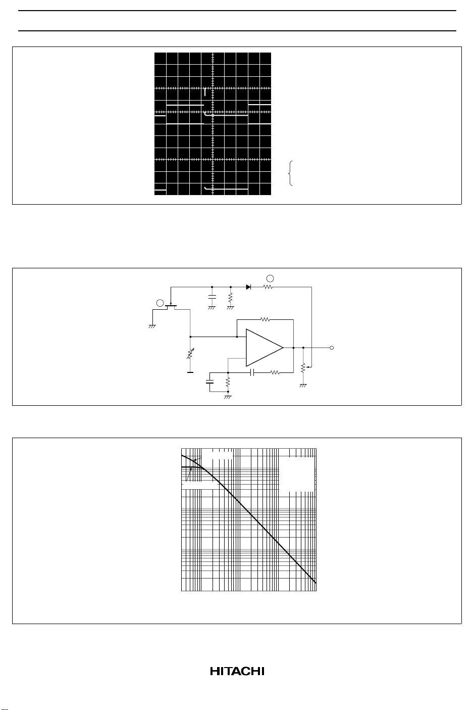
2. Monostable Multivibrator
Figure 3 Monostable Multivibrator Operating Circuit
Trigger input 0
Vin(+) 0
HA17741/PS
R
3
C
1
Input
0
C
2
V
CC
−
+
R
R
2
Vout
V
EE
1
R
L
Figure 4 HA17741 Monostable Multivibrator Operating Waveform
3. Bistable Multivibrator
Vin(−) 0
Vertical:
Horizontal:
Circuit constants
= 10 kΩ, R2 = 2 kΩ
R
Vout 0
Vin(−)
Vin(+)
Input
0
C
V
−
+
V
R
L
R
2
1
= 40 kΩ, C1 = 0.47 µF
R
3
C2 = 0.0068 µF
= ∞
R
L
= 15 V, VEE = −15 V
V
CC
CC
Vout
EE
R
1
Figure 5 Bistable Multivibrator Operating Circuit
5
Page 6
HA17741/PS
Trigger input 0
Vin(+) 0
Vout 0
Figure 6 HA17741 Bistable Multivibrator Operating Waveform
Wien Bridge Sine Wave Oscillator
2SK16 H
Figure 7 Wien Bridge Sine Wave Oscillator
500 Ω
Rin
Vertical:
Horizontal:
5 V/div
2 ms/div
Circuit constants
R1 = 10 kΩ, R2 = 2 kΩ
C = 0.0068 µF
= ∞
R
L
= 15 V, VEE = −15 V
V
CC
1S2074 H
R
1 MΩ
R
C
3
3
4
470 kΩ
5.1 kΩ
R
S
−
+
R
C
R
2
2
1
C
1
R
Vout
50 kΩ
L
30 k
10 k
Oscillator Frequency f (Hz)
V
= 2 V
OP-P
V
= 20 V
OP-P
3 k
1 k
300
100
30
10
30 p 100 p 300 p 1,000 p 3,000 p 0.01 µ 0.03 µ 0.1 µ
VCC = 15 V,
= −15 V
V
EE
= C2/10
C
1
= 110 kΩ,
R
1
= 11 kΩ
R
2
C1 Capacitance (F)
Figure 8 HA17741 Wien Bridge Sine Wave Oscillator f–C Characteristics
6
Page 7

HA17741/PS
Figure 9 HA17741 Wien Bridge Sine Wave Oscillator Operating Waveform
Quadrature Oscillator
Vertical:
Horizontal:
5 V/div
0.5 ms/div
Test circuit condition
VCC = 15 V, VEE = −15 V
= 110 kΩ, R2 = 11 kΩ
R
1
= 0.0015 µF, C2 = 0.015 µF
C
1
Test results
f = 929.7 Hz, T.H.P = 0.06%
Sin out
C
T1
−
+
R
T1
C
1
R
A1
T2
R
1
Cos out
C
T2
−
A2
+
V
4
R
D
1
R
R
D
2
R
V
8
Figure 10 Quadrature Sine Wave Oscillator
11
22
44
33
Figure 10 shows the circuit diagram for a quadrature sine wave oscillator. This circuit consists of two
integrators and a limiter circuit, and provides not only a sine wave output, but also a cosine output, that is,
it also supplies the waveform delayed by 90°. The output amplitude is essentially determined by the limiter
circuit.
7
Page 8

HA17741/PS
f−CT1, CT2, C1 Characteristics
30
CT1 = 102 pF
= 99 pF
C
T2
= 106 pF
C
10
1
3
1.0
0.3
0.1
0.03
0.01
100 p 1,000 p 0.01 µ 0.1 µ
VCC = −VEE = 15 V
= 150 kΩ, RT2 = 150 kΩ
R
T1
= 151.2 kΩ
R
1
= 15 kΩ, R22 = 10 kΩ
R
11
= 15 kΩ, R44 = 10 kΩ
R
33
, CT2, C1 → 1,000 pF
C
T1
Use a Mylar capacitor.
= 21 V
With V
OP-P
= R44 = 10 kΩ
R
22
the frequency of the sine
wave will be under 10 kHz.
and
P-P
Sin out
Cos out
CT1, CT2, C1 (F)
Figure 11 HA17741 Quadrature Sine Wave Oscillator
Triangular Wave Generator
← Sin out
0
← Cos out
Vertical:
Horizontal:
Circuit constants
5 V/div
0.2 ms/div
CT1 = 1000 pF (990), CT2 = 1000 pF (990)
= 150 kΩ, RT2 = 150 kΩ
R
T1
= 1000 pF (990), R1 = 160 kΩ
C
1
= 15 kΩ, R22 = 10 kΩ
R
11
= 16 V, R44 = 10 kΩ
R
33
= 15 V, VEE = −15 V
V
CC
Figure 12 Sine and Cosine Output Waveforms
Integrator
D1R
3
D2R
4
Vout2
Hysteresis comparator
C
−
A1
+
R
1
R
2
+
A2
−
V
R1/R
Vout1
A
2
Figure 13 Triangular Wave Generator Operating Circuit
8
Page 9

0
Vout1
Vout2
0
0
V
A
Figure 14 HA17741 Triangular Wave Generator Operating Waveform
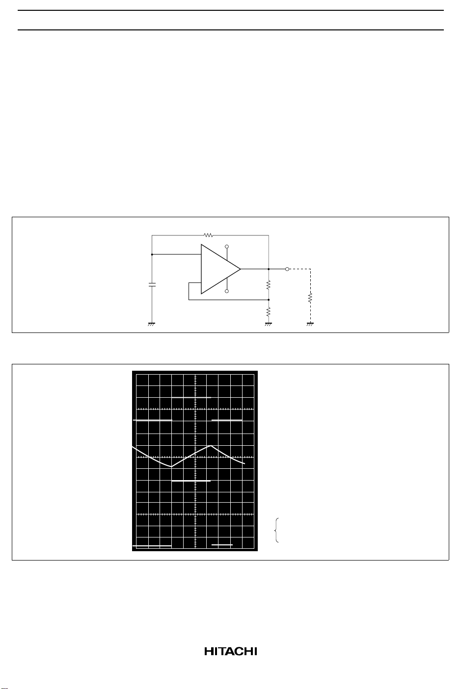
Sawtooth Waveform Generator
Vin
R
6 kΩ
3 kΩ
HA17741/PS
Vertical:
Horizontal:
Circuit constants
R
3
2
V
A
+
−
R
4
2.7 kΩ
2.7 kΩ
6 kΩ
R
V
1
B
R
5
R
6
V
C
2SC1706 H
Q
1
+
−
I
C
1
10 V/div
10 ms/div
= 15 V, VEE = −15 V
V
CC
= 10 kΩ, R2 = 20 kΩ
R
1
= 100 kΩ, R4 = 200 kΩ
R
3
C = 0.1 µF
Vout
R
7
2.7 kΩ
R
8
2.7 kΩ
5 kΩ
V
R
Figure 15 Sawtooth Waveform Generator
V
R
0
Vout
0
Vertical:
Horizontal:
5 V/div
2 ms/div
Circuit constants
VCC = 15 V, VEE = −15 V
= 100 kΩ, C1 = 0.1 µF
R
1
= 10 V
V
in
Figure 16 HA17741 Sawtooth Waveform Generator Operating Waveform
9
Page 10

HA17741/PS
Characteristic Curves
Voltage Offset Adjustment Circuit
R
1
Input Offset Current vs.
Power-Supply Voltage Characteristics
20
R
2
16
(nA)
IO
2
6
3
5
1
12
8
R
R
1
2
R
a = 100%a = 0%
V
EE
Power Dissipation vs.
Power-Supply Voltage Characteristics
100
No load
80
60
40
20
Power dissipation Pd (mW)
0
±3 ±6 ±12 ±15
±9 ±18 ±3 ±6 ±12 ±15
Power-supply voltage VCC, VEE (V)
4
Input offset current I
0
±3 ±6 ±12 ±15
±9 ±18
Power-supply voltage VCC, VEE (V)
Voltage Gain vs.
Power-Supply Voltage Characteristics
120
110
(dB)
VD
100
90
Voltage gain A
80
70
±9 ±18
RL ≥ 2 kΩ
Power-supply voltage VCC, VEE (V)
10
Page 11

HA17741/PS
Maximum Output Voltage Amplitude vs.
Power-Supply Voltage Characteristics
20
RL ≥ 2 kΩ
16
12
(V)
OP-P
±V
8
4
+V
OP-P
OP-P
−V
Maximum output voltage amplitude
0
±3 ±6 ±12 ±15
±9 ±18
Power-supply voltage VCC, VEE (V)
Input Offset Current vs.
Ambient Temperature Characteristics
20
16
(nA)
IO
12
8
4
Input offset current I
0
−20 0 20 40 60
VCC = +15 V
V
Ambient temperature Ta (°C)
= −15 V
EE
Input Offset Voltage vs.
Ambient Temperature Characteristics
5
4
(mV)
IO
3
2
1
Input offset voltage V
0
−20 0 20 40 60
VCC = +15 V
= −15 V
V
EE
≤ 10 kΩ
R
S
80
Ambient temperature Ta (°C)
Input Bias Current vs.
Ambient Temperature Characteristics
120
100
(nA)
IB
80
60
40
Input bias current I
20
0
80
−20 0 20 40 60
VCC = +15 V
= −15 V
V
EE
80
Ambient temperature Ta (°C)
11
Page 12

HA17741/PS
Power Dissipation vs.
Ambient Temperature Characteristics
90
80
70
60
50
Power dissipation Pd (mW)
40
−20 0 20 40 60
VCC = +15 V
= −15 V
V
EE
No load
Ambient temperature Ta (°C)
Maximum Output Voltage Amplitude vs.
Ambient Temperature Characteristics
16
12
8
Voltage Gain vs.
Ambient Temperature Characteristics
120
110
(dB)
VD
100
90
Voltage gain A
80
80
70
−20 0 20 40 60
VCC = +15 V
= −15 V
V
EE
≥ 2 kΩ
R
L
80
Ambient temperature Ta (°C)
Output Shorted Current vs.
Ambient Temperature Characteristics
20
VO = V
CC
VCC = +15 V
= −15 V
16
(mA)
OS
V
EE
4
(V)
0
OP-P
V
−4
−8
Maximum output voltage amplitude
−12
−20 0 40 60
VCC = +15 V
= −15 V
V
EE
= 10 kΩ
R
L
20 80
Ambient temperature Ta (°C)
12
8
4
Output shorted current I
0
−20 0 20 40 60
Ambient temperature Ta (°C)
80
12
Page 13

HA17741/PS
Maximum Output Voltage Amplitude vs.
Load Resistance Characteristics
16
12
8
4
(V)
0
OP-P
V
−4
VCC = +15 V
= −15 V
V
EE
−8
Maximum output voltage amplitude
−12
200 500 1 k 2 k 5 k
10 k
Load resistance RL (Ω)
Maximum Output Voltage Amplitude vs.
Frequency Characteristics
28
24
1.6
VCC = +15 V, VEE = −15 V
R
1.2
See the voltage offset
adjustment circuit diagram.
0.8
0.4
0
−0.4
−0.8
Output voltage Vout (V)
−1.2
−1.6
0
Resistor position a (%)
Input Resistance vs.
Frequency Characteristics
1.4
1.2
Offset Adjustment
Characteristics
= 51 Ω, R2 = 5.1 kΩ
1
R = 10 kΩ
R = 5 kΩ
R = 20 kΩ
20 40 60 80 100
20
16
(V)
12
OP-P
V
VCC = +15 V
8
4
V
EE
= 10 kΩ
R
L
= −15 V
Maximum output voltage amplitude
0
500 1 k 50 k 100 k
200 2 k 5 k 10 k 20 k 200 k 500 k 100 500 1 k 50 k 100 k
100
Frequency f (Hz)
1.0
0.8
0.6
0.4
Input resistance Rin (MΩ)
0.2
0
200 2 k 5 k 10 k 20 k 200 k 500 k 1 M
Frequency f (Hz)
13
Page 14

HA17741/PS
Phase vs.
Frequency Characteristics
40
0
−40
−80
−120
Phase φ (deg.)
−160
−200
−240
50 200 1 k 50 k 100 k
100 2 k 5 k 10 k 20 k 200 k 500 k
500 1 M 2 M
Frequency f (Hz)
Voltage Gain and Phase vs.
Frequency Characteristics (1)
120
100
(dB)
80
VD
60
40
20
0
Voltage gain A
−20
10 50 200 10 k 20 k
20 500 1 k 2 k 5 k 50 k 100 k
100 200 k 500 k 1 M 2 M
VCC = +15 V
= −15 V
V
EE
Closed loop gain = 60 dB
φ
A
VD
Frequency f (Hz)
VCC = +15 V
= −15 V
V
EE
Open loop
0
−60
−120
−180
Phase φ (deg.)
Voltage Gain vs
Frequency Characteristics
120
100
80
(dB)
60
VD
40
20
0
Voltage gain A
−20
40
10 50 200 10 k 20 k
20 500 1 k 2 k 5 k 50 k 100 k
100 500 k 2 M200 k 1 M
Frequency f (Hz)
Voltage Gain and Phase vs.
Frequency Characteristics (2)
120
100
80
(dB)
60
VD
40
20
0
Voltage gain A
−20
−40
10 50 200 10 k 20 k
20 500 1 k 2 k 5 k 50 k 100 k
100 200 k 500 k 1 M 2 M
VCC = +15 V
V
EE
Closed loop gain = 40 dB
Frequency f (Hz)
= −15 V
φ
A
VD
VCC = +15 V
= −15 V
V
EE
Open loop
0
−60
−120
−180
Phase φ (deg.)
14
Page 15

HA17741/PS
Voltage Gain and Phase vs.
Frequency Characteristics (3)
120
100
(dB)
80
VD
VCC = +15 V
60
= −15 V
V
EE
40
Closed loop gain = 20 dB
20
0
Voltage gain A
−20
−40
10 50 200 10 k 20 k
20
500
1 k 2 k 5 k 50 k 100 k100 200 k 500 k 1 M 2 M
Frequency f (Hz)
Impulse Response
Characteristics Test Circuit
2
6
3
Vin
Voltage Gain and Phase vs.
Frequency Characteristics (4)
120
φ
A
VD
0
−60
−120
−180
100
(dB)
80
VD
60
40
20
Phase φ (deg.)
0
Voltage gain A
−20
−40
VCC = +15 V
= −15 V
V
EE
Closed loop gain = 0 dB
10 50 200 10 k 20 k
20
500
1 k 2 k 5 k 50 k 100 k100 200 k 500 k 1 M 2 M
φ
A
VD
0
−60
−120
−180
Phase φ (deg.)
Frequency f (Hz)
Rise time vs.
Power-Supply Voltage Characteristics
0.8
Vin = 20 mV
= 2 kΩ
R
L
= 100 pF
C
Vout
R
C
L
L
0.6
(µs)
r
0.4
L
Vout
90%
10%
V
2
Vout = × 100 (%)
V
V
2
t
r
1
V
1
Rise time t
0.2
0
±3 ±6 ±9 ±12 ±15
Power-supply voltage VCC, VEE (V)
±18
15
Page 16

HA17741/PS
Overshoot vs.
Power-Supply Voltage Characteristics
40
Vin = 20 mV
R
30
20
10
Overshoot Vover (%)
0
±3 ±6 ±9 ±12 ±15
C
Power-supply voltage VCC, VEE (V)
= 2 kΩ
L
= 100 pF
L
±18
Impulse Response
Characteristics
40
30
20
10
0
Output voltage Vout (mV)
0 0.4 0.8 1.2
Time t (µs)
VCC = +15 V
= −15 V
V
EE
= 2 kΩ
R
L
= 100 pF
C
L
= 20 mV
V
in
1.6
16
Page 17

Package Dimensions
0.89
10.6 Max
1
HA17741/PS
Unit: mm
9.6
58
6.3
7.4 Max
4
1.3
2.54 ± 0.25
1.27 Max
0.48 ± 0.10
5.06 Max
0.1 Min
2.54 Min
0° – 15°
Hitachi Code
JEDEC
EIAJ
(reference value)
Mass
7.62
0.25
+ 0.10
– 0.05
DP-8
Conforms
Conforms
0.54 g
17
Page 18

HA17741/PS
Cautions
1. Hitachi neither warrants nor grants licenses of any rights of Hitachi’s or any third party’s patent,
copyright, trademark, or other intellectual property rights for information contained in this document.
Hitachi bears no responsibility for problems that may arise with third party’s rights, including
intellectual property rights, in connection with use of the information contained in this document.
2. Products and product specifications may be subject to change without notice. Confirm that you have
received the latest product standards or specifications before final design, purchase or use.
3. Hitachi makes every attempt to ensure that its products are of high quality and reliability. However,
contact Hitachi’s sales office before using the product in an application that demands especially high
quality and reliability or where its failure or malfunction may directly threaten human life or cause risk
of bodily injury, such as aerospace, aeronautics, nuclear power, combustion control, transportation,
traffic, safety equipment or medical equipment for life support.
4. Design your application so that the product is used within the ranges guaranteed by Hitachi particularly
for maximum rating, operating supply voltage range, heat radiation characteristics, installation
conditions and other characteristics. Hitachi bears no responsibility for failure or damage when used
beyond the guaranteed ranges. Even within the guaranteed ranges, consider normally foreseeable
failure rates or failure modes in semiconductor devices and employ systemic measures such as failsafes, so that the equipment incorporating Hitachi product does not cause bodily injury, fire or other
consequential damage due to operation of the Hitachi product.
5. This product is not designed to be radiation resistant.
6. No one is permitted to reproduce or duplicate, in any form, the whole or part of this document without
written approval from Hitachi.
7. Contact Hitachi’s sales office for any questions regarding this document or Hitachi semiconductor
products.
Hitachi, Ltd.
Semiconductor & Integrated Circuits.
Nippon Bldg., 2-6-2, Ohte-machi, Chiyoda-ku, Tokyo 100-0004, Japan
Tel: Tokyo (03) 3270-2111 Fax: (03) 3270-5109
URL NorthAmerica : http:semiconductor.hitachi.com/
For further information write to:
Hitachi Semiconductor
(America) Inc.
179 East Tasman Drive,
San Jose,CA 95134
Tel: <1> (408) 433-1990
Fax: <1>(408) 433-0223
Europe : http://www.hitachi-eu.com/hel/ecg
Asia (Singapore) : http://www.has.hitachi.com.sg/grp3/sicd/index.htm
Asia (Taiwan) : http://www.hitachi.com.tw/E/Product/SICD_Frame.htm
Asia (HongKong) : http://www.hitachi.com.hk/eng/bo/grp3/index.htm
Japan : http://www.hitachi.co.jp/Sicd/indx.htm
Hitachi Europe GmbH
Electronic components Group
Dornacher Straβe 3
D-85622 Feldkirchen, Munich
Germany
Tel: <49> (89) 9 9180-0
Fax: <49> (89) 9 29 30 00
Hitachi Europe Ltd.
Electronic Components Group.
Whitebrook Park
Lower Cookham Road
Maidenhead
Berkshire SL6 8YA, United Kingdom
Tel: <44> (1628) 585000
Fax: <44> (1628) 778322
Hitachi Asia Pte. Ltd.
16 Collyer Quay #20-00
Hitachi Tower
Singapore 049318
Tel: 535-2100
Fax: 535-1533
Hitachi Asia Ltd.
Taipei Branch Office
3F, Hung Kuo Building. No.167,
Tun-Hwa North Road, Taipei (105)
Tel: <886> (2) 2718-3666
Fax: <886> (2) 2718-8180
Copyright ' Hitachi, Ltd., 1998. All rights reserved. Printed in Japan.
18
Hitachi Asia (Hong Kong) Ltd.
Group III (Electronic Components)
7/F., North Tower, World Finance Centre,
Harbour City, Canton Road, Tsim Sha Tsui,
Kowloon, Hong Kong
Tel: <852> (2) 735 9218
Fax: <852> (2) 730 0281
Telex: 40815 HITEC HX
 Loading...