

Page 1
HA17558 Serise
Dual Operational Amplifier
Description
HA17558 is dual operational amplifiers which provides internal frequency compensation and high
performance. It can be applied widely to measuring control equipment and to general Use. The two
amplifiers share a common bias network and power supply leads.
Features
• High voltage Gain: 104dB (Typ)
• High speed: 1V/µs
• Continuous short-circuit protection
• Low-noise operational amplifiers
• Internal frequency compensation
Ordering Information
Type No. Application Package
HA17558FP Industrial use FP-8D
HA17558F Commercial use FP-8D
HA17558 Commercial use DP-8
HA17558PS Industrial use DP-8
Page 2
HA17558 Serise
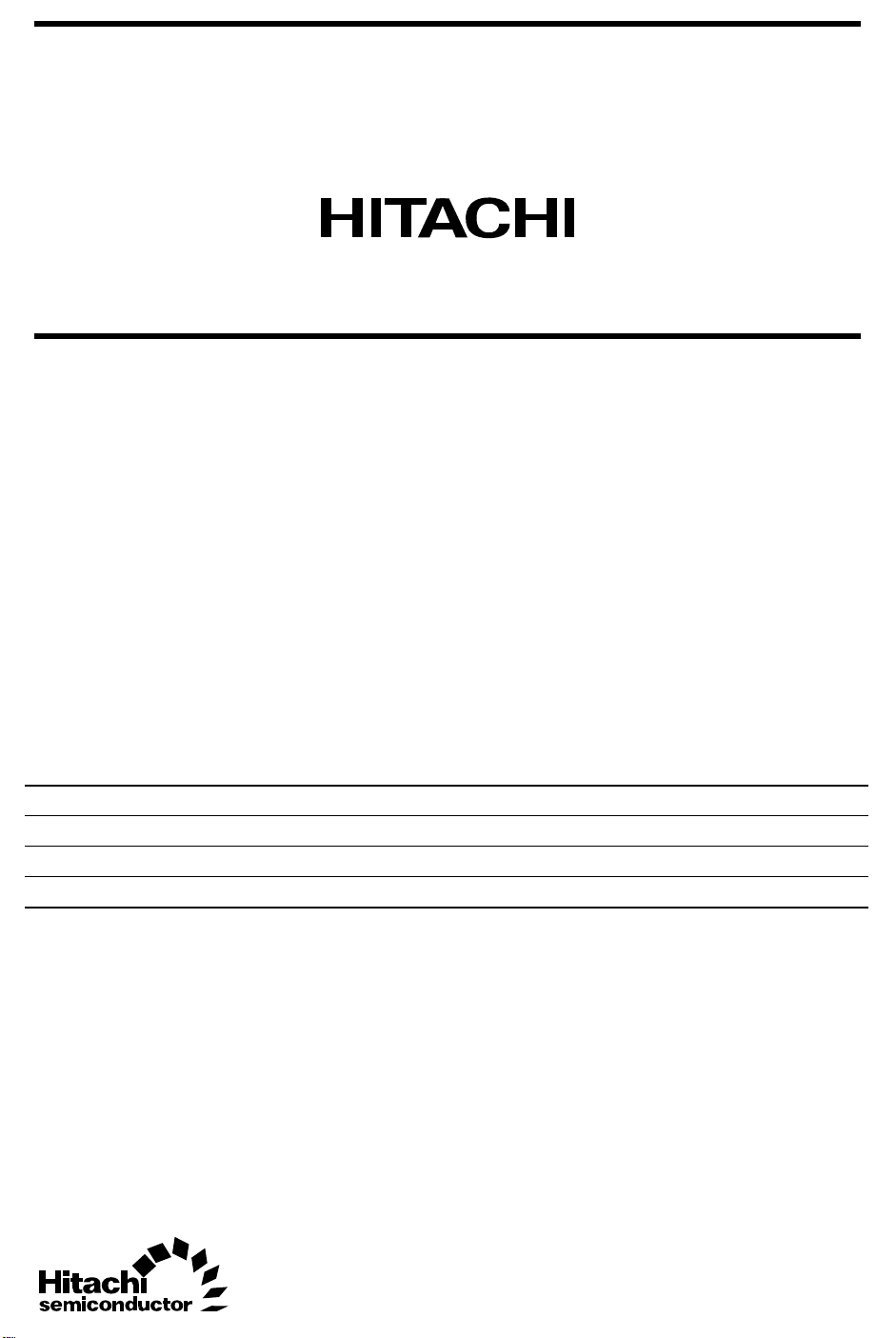
Pin Arrangement
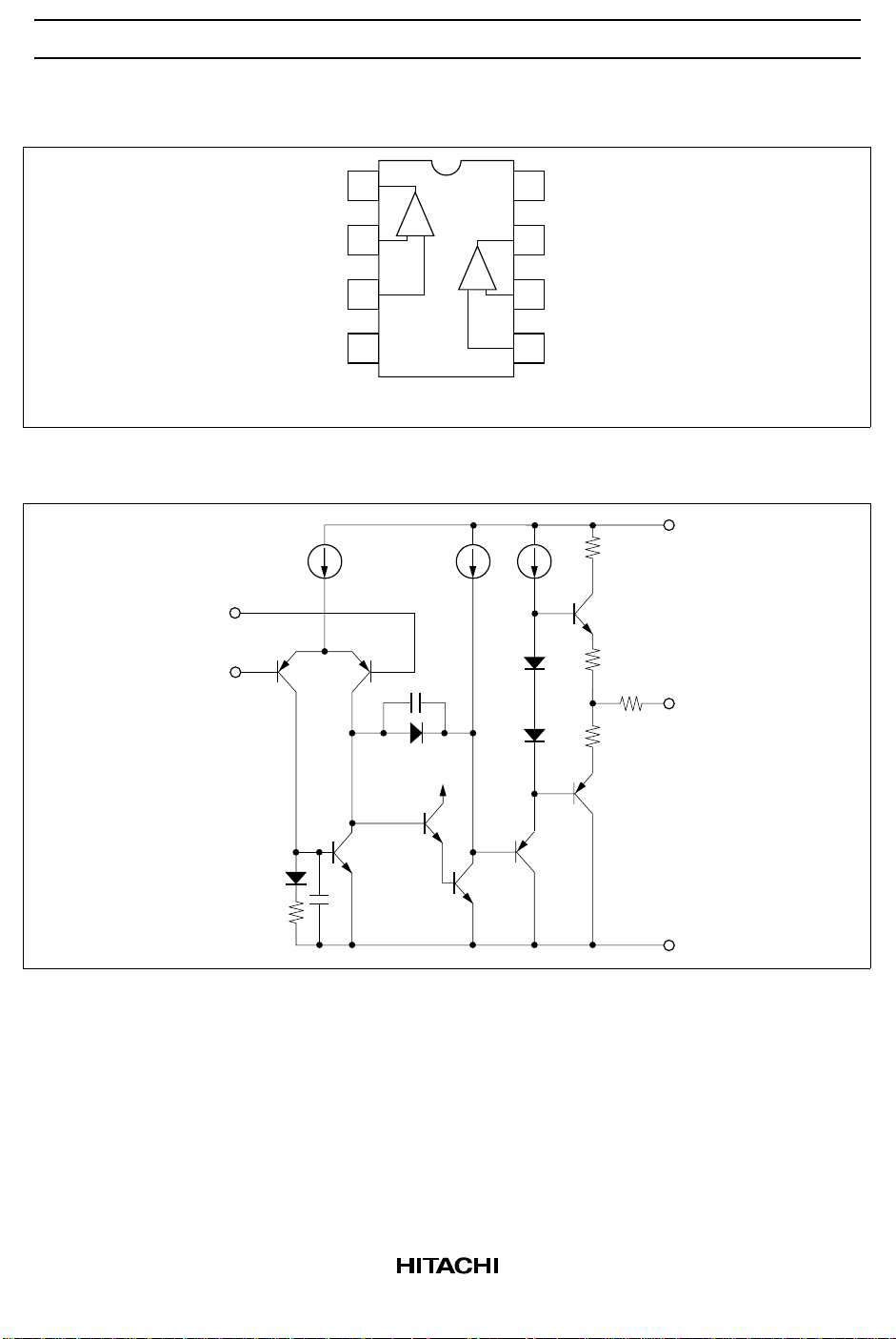
Circuit Schematic (1/2)
Vin(+)
Vin(–)
Vout1
Vin(–)1
Vin(+)1
V
EE
1
2
3
4
1
–+
(Top View)
2
+–
8
7
6
5
V
CC
Vout2
Vin(–)2
Vin(+)2
V
CC
out
V
to V
CC
V
EE
2
Page 3
HA17558 Serise
Absolute Maximum Ratings (Ta = 25°C)
Ratings
HA17558 HA17558PSHA17558FHA17558
Item Symbol
Supply voltage V
Differential input voltage V
V
CC
EE
IN (diff)
Common-mode input voltage VCM*
Power dissipation P
T
3
+18 +18 +18 +18 V
–18 –18 –18 –18 V
±30 ±30 ±30 ±30 V
±15 ±15 ±15 ±15 V
670*
Operating temperature Topr –20 to
+75
Storage temperature Tstg –55 to
+125
1
670*
–20 to
+75
–55 to
+125
1
385*
2
–20 to
+75
–55 to
+125
FP
385*
–20 to
+75
–55 to
+125
2
Notes: 1. These are the allowable values up to Ta = 45 °C. Derate by 8.3mW/°C above that temperature.
2. These are the allowable values up to Ta = 31 °C mounting on 30% wiring density glass epoxy
board. Derate by 7.14mW/°C above that temperature.
3. If the supply voltage is less than ±15V, input voltage should be less than supply voltage.
Unit
mW
–20 to
+75
°C
Electrical Characteristics (Ta = 25°C, VCC = +15V, VEE = –15V)
Item Symbol Min Typ Max Unit Test conditions
Input offset voltage V
Input offset current I
Input bias current I
Voltage gain A
IO
IO
IB
VD
Maximum output voltage Vop-p ±12 ±14 — V RL ≥ 10kΩ
Maximum output voltage Vop-p ±10 ±12.4 — V RL ≥ 2kΩ
Common mode input voltage
V
CM
range
Common mode rejection ratio CMR 70 100 — dB RS ≤ 10kΩ
Supply voltage rejection ratio PSRR — 10 150 µV/V RS ≤ 10kΩ
Power dissipation Pd — 90 170 mW 2-channel, No load
Slew rate SR — 1.0 — V/µsAVD = 1
Equivalent input noise voltage V
NI
Channel separation CS — 105 — dB f = 1kHz
— 0.5 6 mV RS ≤ 10kΩ
— 5 200 nA
— 50 500 nA
86 104 — dB RL ≥ 2kΩ, VO = ±10V
±12 ±14 — V
—6 —µVp-p RS = 1kΩ, f = 1HZ to 1kH
Z
3
Page 4
HA17558 Serise
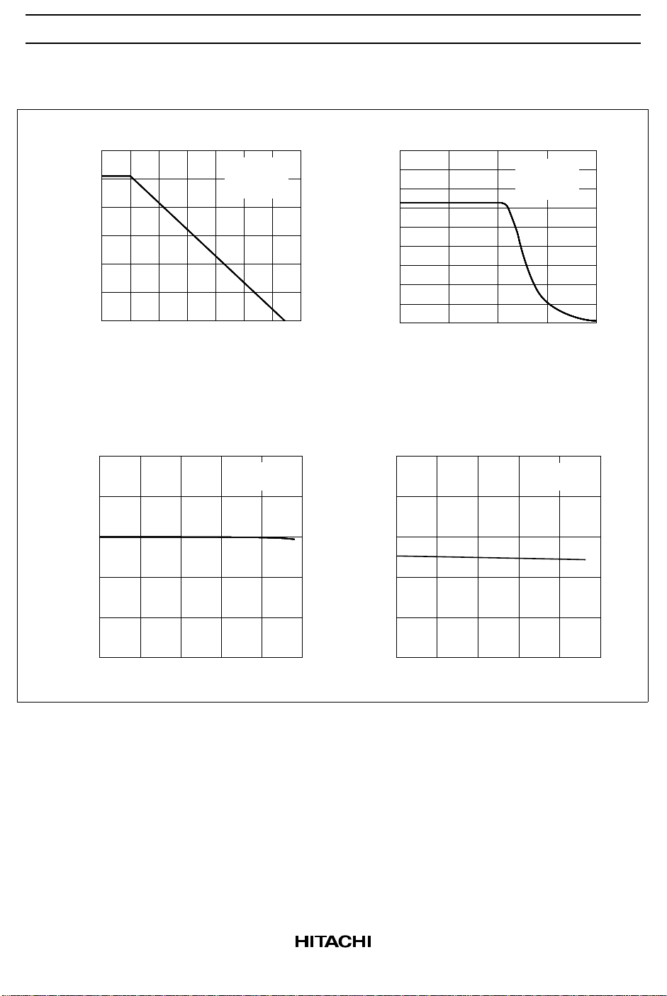
Characteristic Curves
Open Loop Voltage Gain vs. Frequency
120
(dB)
100
V(OL)
VCC = 15 V
V
EE
R
= 2 kΩ
L
80
60
40
20
0
Open Loop Voltage Gain A
1 10 100 1 k 10 k 100 k 1 M 10 M
Frequency f (Hz)
Power Supply Rejection Ratio
vs. Ambient Temperature
120
VCC = 15 V
V
110
EE
100
= –15 V
= –15 V
Maximum Output Voltage vs. Frequency
36
(V)
32
OP-P
28
VCC = 15 V
V
R
24
20
16
12
8
4
0
Maximum Output Voltage V
100
1 k 10 k 100 k 1 M
Frequency f (Hz)
Voltage Gain vs. Ambient Temperature
130
120
(dB)
VD
110
= –15 V
EE
= 2 kΩ
L
VCC = 15 V
= –15 V
V
EE
90
80
70
Power Supply Rejection Ratio PSRR (dB)
–20
0 20406080
Ambient Temperature Ta (°C)
4
100
Voltage Gain A
90
80
–20
Ambient Temperature Ta (°C)
0 20406080
Page 5

Power Supply Rejection Ratio vs. Frequency
HA17558 Serise
120
100
80
60
40
20
Power Supply Rejection Ratio PSRR (dB)
0
100
300 1 k 3 k 10 k 30 k 100 k 300 k 1 M
Frequency f (Hz)
Common-mode Rejection Ratio vs. Frequency
120
100
80
VCC = 15 V
V
= –15 V
EE
VCC = 15 V
V
= –15 V
EE
Ta = 25°C
R
= ∞
L
60
40
20
Common–mode Rejection Ratio CMR (dB)
0
100
300 1 k 3 k 10 k 30 k 100 k 300 k
Frequency f (Hz)
1 M
5
Page 6

HA17558 Serise
Transient Response
(V)
O
10
5
V
= 15 V
CC
V
= –15 V
EE
0
–5
Output Voltage V
–10
010203040
Time t (µs)
Power Dissipation vs. Ambient Temperature
100
VCC = 15 V
VEE = –15 V
90
RL = ∞
80
70
Maximum Output Voltage
vs. Ambient Temperature
40
)
P-P
(V
OP-P
32
VCC = 15 V
VEE = –15 V
RL = 2 kΩ
24
16
8
Maximum Output Voltage V
0
–20 0 20 40
60
Ambient Temperature Ta (°C)
Maximum Output Voltage vs. Load Resistance
)
30
P-P
(V
25
OP-P
VCC = 15 V
20
VEE = –15 V
f = 1 kHz
15
80
60
Power Dissipation Pd (mW)
50
–200 20406080
Ambient Temperature Ta (°C)
6
10
Maximum Output Voltage V
5
100 200 500 1 k 2 k 5 k 10 k
Load Resistance R
(Ω)
L
Page 7

HA17558 Serise
Supply Current vs. Supply Voltage
5
RL = ∞
4
(mA)
CC
3
2
Supply Current I
1
0
±4 ±6 ±9 ±12 ±15 ±18
Supply Voltage VCC, V
EE
(V)
Input Bias Current vs. Ambient Temperature
100
VCC = 15 V
= –15 V
V
80
(nA)
IB
EE
60
40
20
Input Bias Current I
0
–20 0 20 40 60
Ambient Temperature Ta (°C)
80
Common-mode Input Voltage vs.
Supply Voltage
20
(V)
CM
10
0
–10
Common-mode Input Voltage V
–20
±4 ±8 ±12 ±16 ±18
Supply Voltage V
, VEE (V)
CC
Slew Rate vs. Supply Voltage
1.2
1.0
0.8
0.6
Slew Rate SR (V/µs)
0.4
f = 1 kHz
R
L
C
L
Ta = 25°C
A
V
±4 ±6 ±9 ±12 ±18
Supply Voltage V
, VEE (V)
CC
= 2 kΩ
= 100 pF
= 1
±15
7
Page 8

HA17558 Serise
Input Offset Current vs. Ambient Temperature
40
20
(nA)
IO
0
VCC = 15 V
V
= –15 V
EE
Input Offset Voltage vs. Supply Voltage
4
(mV)
IO
2
–20
–40
Input Offset Current I
–20
02040 80
Ambient Temperature Ta (°C)
Voltage Gain vs. Supply Voltage
120
100
(dB)
VD
80
60
Voltage Gain A
40
–4 –6 –9 –12 –15
Supply Voltage V
, VEE (V)
CC
60
f = 10 Hz
= 2 kΩ
R
L
–18
0
–2
Input Offset Voltage V
–4
–4 –6 –9 –12 –15
–18
Supply Voltage VCC, VEE (V)
Slew Rate vs. Ambient Temperature
1.4
VCC = 15 V
V
= –15 V
1.2
1.0
EE
R
= 2 kΩ
L
= 100 pF
C
L
A
= 1
V
0.8
Slew Rate SR (V/µs)
0.6
0.4
–200 20406080
Ambient Temperature Ta (°C)
8
Page 9

Output Short Current vs. Ambient Temperature
60
50
(mA)
OS
40
VCC = 15 V
V
= –15 V
EE
Sink
HA17558 Serise
100
√
30
(nV/ Hz)
NI
10
30
Source
20
Output Short Current I
10
–200 20406080
Ambient Temperature Ta (°C)
Input Noise Voltage vs. Frequency
RS = 100 Ω
3
Input Noise Voltage V
1
10 30 100 300 1 k
Frequency f (Hz)
3 k 10 k
9
Page 10

HA17558 Serise
Input Offset Voltage vs. Ambient Temperature
4
(mA)
IO
2
0
–2
Input Offset Voltage V
–4
–200 20406080
Ambient Temperature Ta (°C)
VCC = 15 V
V
= –15 V
EE
Common-mode Rejection Ratio
140
120
100
80
60
40
Common-mode Rejection Ratio CMR (dB)
–20 0 20 40 60 80
vs. Ambient Temperature
VCC = 15 V
V
= –15 V
EE
Ambient Temperature Ta (°C)
10
Page 11

Circuit Example
HA17558 Serise
33 µF
2.2 kΩInput
56 kΩ
T.H.D. vs. Output Voltage (RIAA Pre-Amp)
1.0
0.3
RIAA Pre-amplifier
0.0022 µF 0.01 µF
36 kΩ 390 kΩ
–
HA17558
+
+
47 µF
–
1 kΩ
–15 V
60
50
+15 V
+
100 µF
–
33 µF
–
100 µF
+
T.H.D. vs. Output Voltage (RIAA Pre–Amp)
Otuput
10 kΩ
VCC = 15 V
V
= –15 V
EE
0.1
0.03
T.H.D (%)
0.01
0.003
0.001
0.01 0.03 0.1 0.3 31.0 10
Output Voltage (Vrms)
20 kHz
10 kHz
1 kHz
20 kHz
40
(dB)
VD
30
20
Voltage Gain A
10
0
10 30 100 300 1 k 3 k 10 k 30 k 100 k
Frequency f (Vrms)
11
Page 12

HA17558 Serise
Package Dimensions
0.89
10.6 Max
1
Unit: mm
9.6
58
6.3
7.4 Max
4
1.3
2.54 ± 0.25
1.27 Max
8
1
1.27
0.48 ± 0.10
4.85
5.25 Max
0.75 Max
5
4
5.06 Max
0.1 Min
2.54 Min
4.4
2.03 Max
0° – 15°
Hitachi Code
JEDEC
EIAJ
Mass
6.50
0.20 ± 0.04
*0.22 ± 0.05
0.60
7.62
0.25
(reference value)
+ 0.25
– 0.15
1.05
0° – 8°
+ 0.25
– 0.18
+ 0.10
– 0.05
DP-8
Conforms
Conforms
0.54 g
Unit: mm
*0.42 ± 0.08
*Dimension including the plating thickness
Base material dimension
12
0.40 ± 0.06
0.10 ± 0.10
0.12
0.15
M
Hitachi Code
JEDEC
EIAJ
(reference value)
Mass
FP-8D
—
Conforms
0.10 g
Page 13

HA17558 Serise
Cautions
1. Hitachi neither warrants nor grants licenses of any rights of Hitachi’s or any third party’s patent,
copyright, trademark, or other intellectual property rights for information contained in this document.
Hitachi bears no responsibility for problems that may arise with third party’s rights, including
intellectual property rights, in connection with use of the information contained in this document.
2. Products and product specifications may be subject to change without notice. Confirm that you have
received the latest product standards or specifications before final design, purchase or use.
3. Hitachi makes every attempt to ensure that its products are of high quality and reliability. However,
contact Hitachi’s sales office before using the product in an application that demands especially high
quality and reliability or where its failure or malfunction may directly threaten human life or cause risk
of bodily injury, such as aerospace, aeronautics, nuclear power, combustion control, transportation,
traffic, safety equipment or medical equipment for life support.
4. Design your application so that the product is used within the ranges guaranteed by Hitachi particularly
for maximum rating, operating supply voltage range, heat radiation characteristics, installation
conditions and other characteristics. Hitachi bears no responsibility for failure or damage when used
beyond the guaranteed ranges. Even within the guaranteed ranges, consider normally foreseeable
failure rates or failure modes in semiconductor devices and employ systemic measures such as failsafes, so that the equipment incorporating Hitachi product does not cause bodily injury, fire or other
consequential damage due to operation of the Hitachi product.
5. This product is not designed to be radiation resistant.
6. No one is permitted to reproduce or duplicate, in any form, the whole or part of this document without
written approval from Hitachi.
7. Contact Hitachi’s sales office for any questions regarding this document or Hitachi semiconductor
products.
Hitachi, Ltd.
Semiconductor & Integrated Circuits.
Nippon Bldg., 2-6-2, Ohte-machi, Chiyoda-ku, Tokyo 100-0004, Japan
Tel: Tokyo (03) 3270-2111 Fax: (03) 3270-5109
URL NorthAmerica : http:semiconductor.hitachi.com/
For further information write to:
Hitachi Semiconductor
(America) Inc.
179 East Tasman Drive,
San Jose,CA 95134
Tel: <1> (408) 433-1990
Fax: <1>(408) 433-0223
Europe : http://www.hitachi-eu.com/hel/ecg
Asia (Singapore) : http://www.has.hitachi.com.sg/grp3/sicd/index.htm
Asia (Taiwan) : http://www.hitachi.com.tw/E/Product/SICD_Frame.htm
Asia (HongKong) : http://www.hitachi.com.hk/eng/bo/grp3/index.htm
Japan : http://www.hitachi.co.jp/Sicd/indx.htm
Hitachi Europe GmbH
Electronic components Group
Dornacher Straβe 3
D-85622 Feldkirchen, Munich
Germany
Tel: <49> (89) 9 9180-0
Fax: <49> (89) 9 29 30 00
Hitachi Europe Ltd.
Electronic Components Group.
Whitebrook Park
Lower Cookham Road
Maidenhead
Berkshire SL6 8YA, United Kingdom
Tel: <44> (1628) 585000
Fax: <44> (1628) 778322
Hitachi Asia Pte. Ltd.
16 Collyer Quay #20-00
Hitachi Tower
Singapore 049318
Tel: 535-2100
Fax: 535-1533
Hitachi Asia Ltd.
Taipei Branch Office
3F, Hung Kuo Building. No.167,
Tun-Hwa North Road, Taipei (105)
Tel: <886> (2) 2718-3666
Fax: <886> (2) 2718-8180
Copyright ' Hitachi, Ltd., 1998. All rights reserved. Printed in Japan.
Hitachi Asia (Hong Kong) Ltd.
Group III (Electronic Components)
7/F., North Tower, World Finance Centre,
Harbour City, Canton Road, Tsim Sha Tsui,
Kowloon, Hong Kong
Tel: <852> (2) 735 9218
Fax: <852> (2) 730 0281
Telex: 40815 HITEC HX
13
 Loading...