

Page 1

HA16114P/PJ/FP/FPJ, HA16120FP/FPJ
Switching Regulator for Chopper Type DC/DC Converter
Description
The HA16114P/FP/FPJ and HA16120FP/FPJ are single-channel PWM switching regulator controller ICs
suitable for chopper-type DC/DC converters. Integrated totem-pole output circuits enable these ICs to
drive the gate of a power MOSFET directly. The output logic of the HA16120 is designed to control a
DC/DC step-up (boost) converter using an N-channel power MOS FET. The output logic of the HA16114
is designed to control a DC/DC step-down (buck) converter or inverting converter using a P-channel power
MOS FET.
These ICs can operate synchronously with external pulse, a feature that makes them ideal for power
supplies that use a primary-control AC/DC converter to convert commercial AC power to DC, then use one
or more DC/DC converters on the secondary side to obtain multiple DC outputs. Synchronization is with
the falling edge of the ‘sync’ pulse, which can be the secondary output pulse from a flyback transformer.
Synchronization eliminates the beat interference that can arise from different operating frequencies of the
AC/DC and DC/DC converters, and reduces harmonic noise. Synchronization with an AC/DC converter
using a forward transformer is also possible, by inverting the ‘sync’ pulse.
Overcurrent protection features include a pulse-by-pulse current limiter that can reduce the width of
individual PWM pulses, and an intermittent operating mode controlled by an on-off timer. Unlike the
conventional latched shutdown function, the intermittent operating function turns the IC on and off at
controlled intervals when pulse-by-pulse current limiting continues for a programmable time. This results
in sharp vertical settling characteristics. Output recovers automatically when the overcurrent condition
subsides.
Using these ICs, a compact, highly efficient DC/DC converter can be designed easily, with a reduced
number of external components.
Functions
• 2.5 V voltage reference
• Sawtooth oscillator (Triangle wave)
• Overcurrent detection
• External synchronous input
• Totem-pole output
• Undervoltage lockout (UVL)
Page 2

HA16114P/PJ/FP/FPJ, HA16120FP/FPJ
• Error amplifier
• Vref overvoltage protection (OVP)
Features
• Wide supply voltage range: 3.9 V to 40 V*
• Maximum operating frequency: 600 kHz
• Able to drive a power MOS FET (±1 A maximum peak current) by the built-in totem-pole gate pre-
driver circuit
• Can operate in synchronization with an external pulse signal, or with another controller IC
• Pulse-by-pulse overcurrent limiting (OCL)
• Intermittent operation under continuous overcurrent
• Low quiescent current drain when shut off by grounding the ON/OFF pin
HA16114: I
HA16120: I
• Externally trimmable reference voltage (Vref): ±0.2 V
• Externally adjustable undervoltage lockout points (with respect to VIN)
• Stable oscillator frequency
• Soft start and quick shut function
= 10 µA (max)
OFF
= 150 µA (max)
OFF
Note: The reference voltage 2.5 V is under the condition of VIN ≥ 4.5 V.
Ordering Information
Hitachi Control ICs for Chopper-Type DC/DC Converters
Product Channel Control Functions Overcurrent
Channels Number No. Step-Up Step-Down Inverting Output Circuits Protection
Dual HA17451 Ch 1 ❍❍ ❍Open collector SCP with timer (latch)
Ch 2 ❍❍ ❍
Single HA16114 —— ❍❍Totem pole Pulse-by-pulse
HA16120 — ❍ — — power MOS FET current limiter and
Dual HA16116 Ch 1 — ❍❍driver intermittent operation
Ch 2 — ❍ — by on/off timer
HA16121 Ch 1 — ❍❍
Ch 2 ❍ ——
2
Page 3
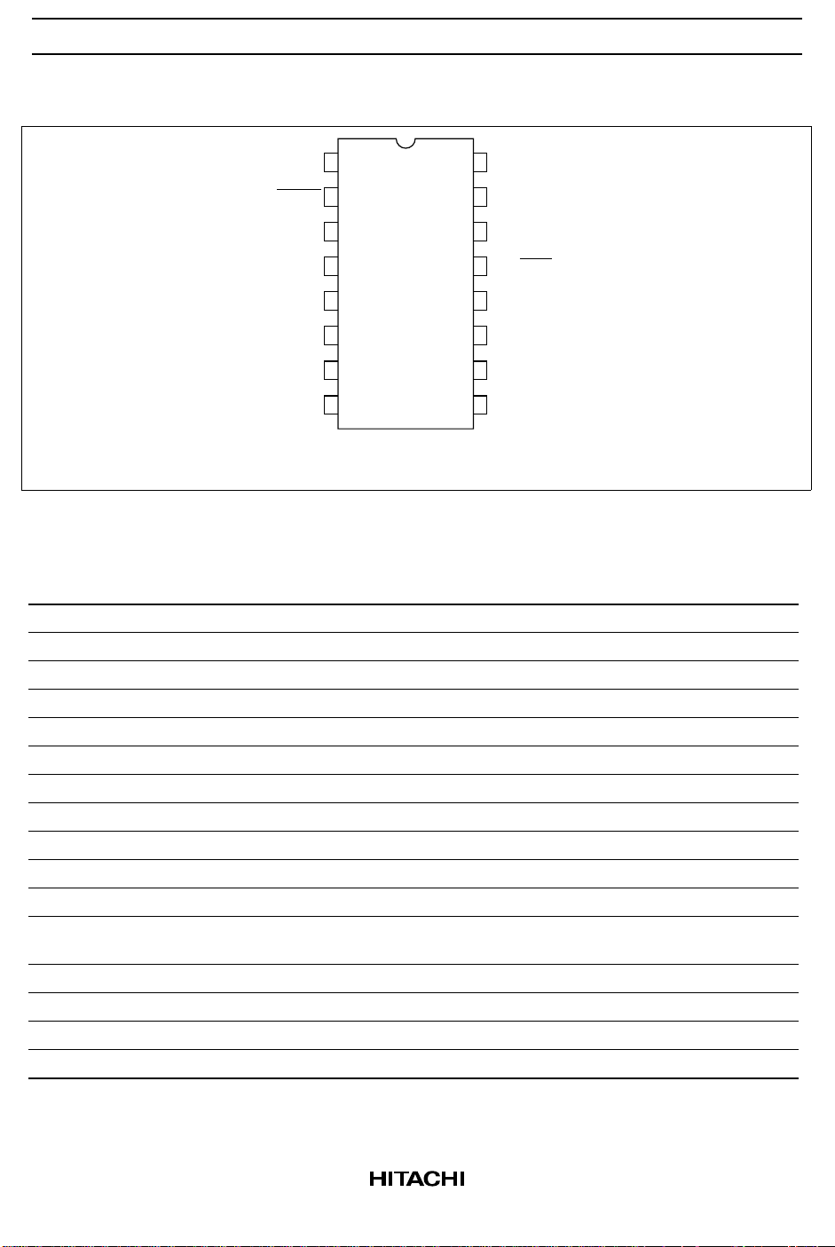
Pin Arrangement
GND*
HA16114P/PJ/FP/FPJ, HA16120FP/FPJ
1
116
Vref
SYNC
IN(−)
IN(+)
P.GND*
215
314
R
T
C
413
T
512
E/O
611
710
1
8
ADJ
DB
ON/OFF
TM
CL(−)
V
IN
OUT9
(Top view)
Note: 1. Pin 1 (GND) and Pin 8 (P.GND) must be connected each other with external wire.
Pin Description
Pin No. Symbol Function
1 GND Signal ground
2 SYNC External sync signal input (synchronized with falling edge)
3R
4C
T
T
5 IN(–) Inverting input to error amplifier
6 E/O Error amplifier output
7 IN(+) Non-inverting input to error amplifier
8 P.GND Power ground
9 OUT Output (pulse output to gate of power MOS FET)
10 V
IN
11 CL(–) Inverting input to current limiter
12 TM Timer setting for intermittent shutdown when overcurrent is detected (sinks
13 ON/OFF IC on/off control (off below approximately 0.7 V)
14 DB Dead-band duty cycle control input
15 ADJ Reference voltage (Vref) adjustment input
16 Vref 2.5 V reference voltage output
Oscillator timing resistor connection (bias current control)
Oscillator timing capacitor connection (sawtooth voltage output)
Power supply input
timer transistor current)
3
Page 4
HA16114P/PJ/FP/FPJ, HA16120FP/FPJ
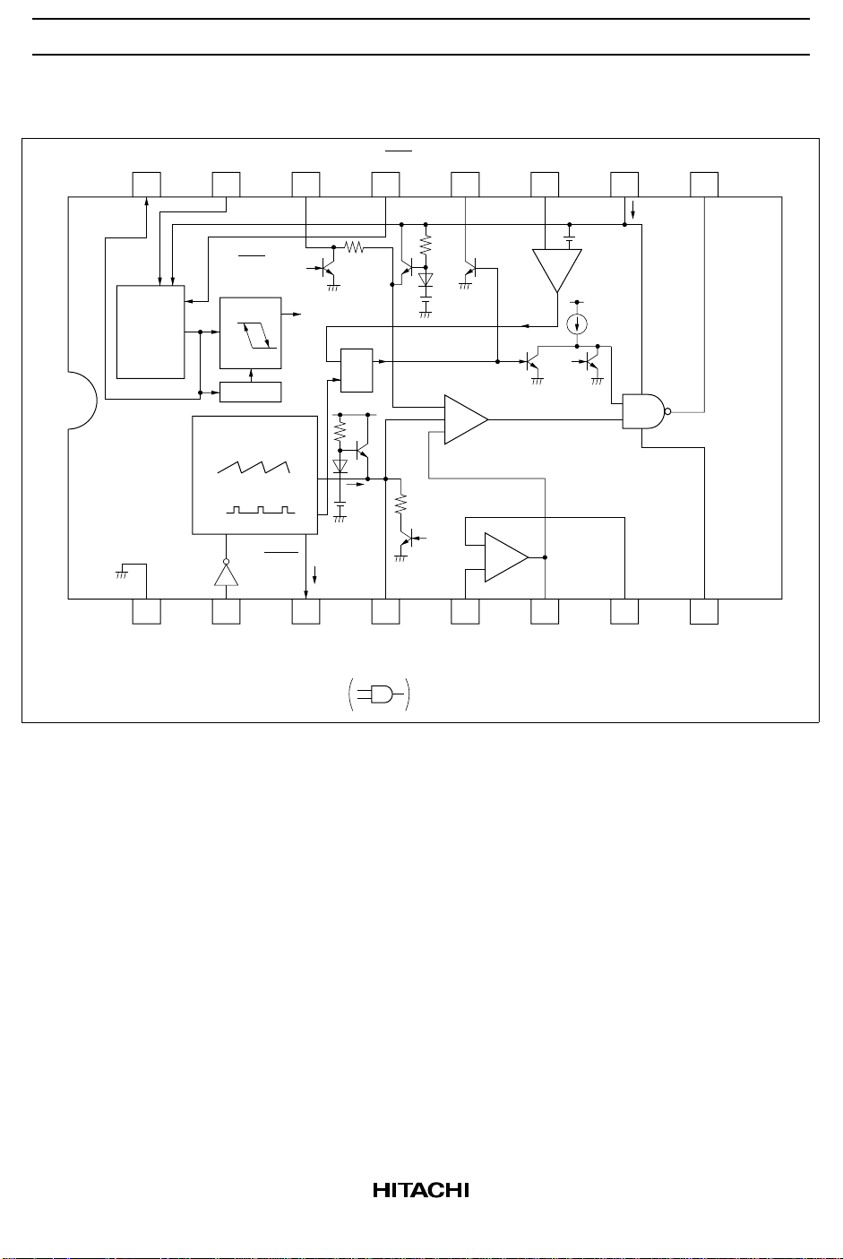
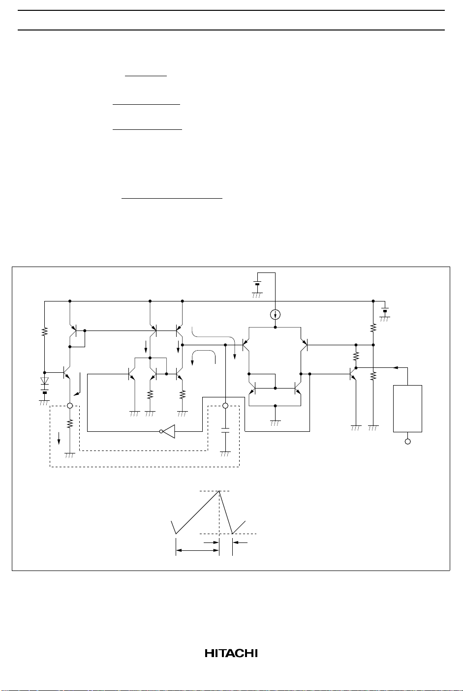
Block Diagram
Vref ADJ DB ON/OFF TM CL(−)V
IN
OUT
16 15 14 13 12 11 10 9
0.2 V
+
−
EA
− +
CL
from
UVL
Vref
*1
OUT
NAND (HA16114)
ADJ V
2.5V
bandgap
reference
voltage
generator
IN
ON/OFF
from
UVL
UVL
H
L
V
LVH
OVP
Triangle waveform
generator
1.6 V
1.0 V
Latch reset pulses
1.1 V
R
Bias
UVL
output
T
1k
Latch
SRQ
V
IN
0.3 V
0.3V
PWM COMP
+
−
+
1k
from
UVL
current
12345678
GND
SYNC R C IN(−) E/O IN(+) P.GND
TT
Note: 1. The HA16120 has an AND gate.
4
Page 5
HA16114P/PJ/FP/FPJ, HA16120FP/FPJ
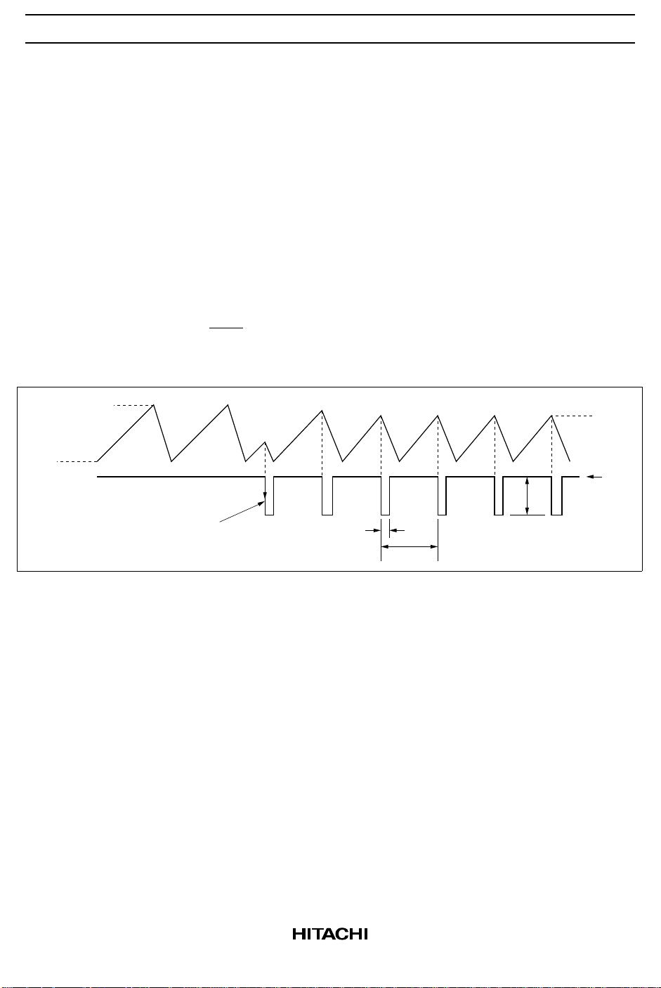
Timing Waveforms
Generation of PWM pulse output from sawtooth wave (during steady-state operation)
Dead-band
voltage (at DB)
Sawtooth wave
(at C )
T
Error amplifier
output (at E/O)
HA16114 PWM
pulse output
(drives gate of
P-channel
power MOS FET)
V
IN
0 V
Off
Off Off Off
1.6 V typ
1.0 V
typ
On On On OnOn
T =
1
f
OSC
Off
HA16120 PWM
pulse output
(drives gate of
N-channel
power MOS FET)
Note: On duty =
V
IN
0 V
Off Off Off OffOff
On On On OnOn
Time t
t
ON
T
5
Page 6
HA16114P/PJ/FP/FPJ, HA16120FP/FPJ
Guide to the Functional Description
The description covers the topics indicated below.
Oscillator
frequency
1.
(f ) control and
OSC
synchronization
DC/DC output
voltage setting
2.
and error
amplifier usage
Dead-band and
3.
soft-start settings
Output stage and
4.
power MOS FET
driving method
Note: 1.
P.GND is a high-current (±1 A maximum peak) ground pin connected to the totem-pole output circuit.
GND is a low-current ground pin connected to the Vref voltage reference. Both pins must be grounded.
P.GND*
GND*
SYNC
IN(−)
E/O
IN(+)
1
R
T
C
T
1
1. Sawtooth Oscillator (Triangle Wave)
1
2
3
4
5
6
7
8
(Top view)
16
15
14
13
12
11
10
Vref adjustment,
Vref
ADJ
DB
ON/OFF
TM
CL(−)
V
IN
OUT
9
undervoltage
lockout, and
5.
overcurrent
protection
ON/OFF pin
6.
usage
Intermittent
mode timing
7.
during
overcurrent
Setting of
8.
current limit
1.1 Operation and Frequency Control
The sawtooth wave is a voltage waveform from which the PWM pulses are created (See figure 1). The
sawtooth oscillator operates as follows. A constant current IO determined by an external timing resistor R
is fed continuously to an external timing capacitor CT. When the CT pin voltage exceeds a comparator
threshold voltage VTH, the comparator output opens a switching transistor, allowing a 3IO discharge current
to flow from CT. When the CT pin voltage drops below a threshold voltage VTL, the comparator output
closes the switching transistor, stopping the 3IO discharge. Repetition of these operations generates a
sawtooth wave.
The value of IO is 1.1 V/RT Ω . The IO current mirror has a limited current capacity, so RT should be at least
5 kΩ (IO ≤ 220 µA).
Internal resistances RA, RB, and RC set the peak and valley voltages VTH and VTL of the sawtooth waveform
at approximately 1.6 V and 1.0 V.
6
T
Page 7
HA16114P/PJ/FP/FPJ, HA16120FP/FPJ
The oscillator frequency f
f
OSC
Here,
t
=
1
t2 =
can be calculated as follows.
OSC
=
1
t
+ t2 + t
1
C
× (VH − VL)
T
1.1 V/R
C
× (VH − VL)
T
3 × 1.1 V/R
3
T
T
t3 ≈ 0.8 µs (comparator delay time)
Since
VH − VL = 0.6 V
f
≈
OSC
0.73 × C
1
× RT + 0.8 (µs)
T
(Hz)
At high frequencies the comparator delay causes the sawtooth wave to overshoot the 1.6 V threshold and
undershoot the 1.0 V threshold, and changes the dead-band thresholds accordingly. Select constants by
testing under implementation conditions.
3.2 V
1.1 V
Current
mirror
(Internal voltage)
1 : 4
C charging
T
I
O
Discharg
-ing 3I
O
Oscillator
comparator
R
C
Vref
2.5 V
R
A
R
B
Sync
circuit
R
T
C
T
I
O
External circuit
V = 1.6 V typ
H
t
2
t
1
V = 1.0 V typ
L
t1 : t2 = 3 : 1
SYNC
Figure 1.1 Equivalent Circuit of Oscillator
7
Page 8
HA16114P/PJ/FP/FPJ, HA16120FP/FPJ
1.2 External Synchronization
These ICs have a sync input pin so that they can be synchronized to a primary-control AC/DC converter.
Pulses from the secondary winding of the switching transformer should be dropped through a resistor
voltage divider to the sync input pin. Synchronization takes place at the falling edge, which is optimal for
multiple-output power supplies that synchronize with a flyback AC/DC converter.
The sync input pin (SYNC) is connected internally through a synchronizing circuit to the sawtooth
oscillator to synchronize the sawtooth waveform (see figure 1.2).
• Synchronization is with the falling edge of the external sync signal.
• The frequency of the external sync signal must be in the range f
• The duty cycle of the external sync signal must be in the range 5% < t1/t2 < 50% (t1 = 300 ns Min).
• With external synchronization, VTH' can be calculated as follows.
f
VTH’ = (VTH − VTL) × + V
OSC
f
SYNC
TL
Note: When not using external synchronization, connect the SYNC pin to the Vref pin.
V (1.6 V typ)
TH
Sawtooth wave
(f
)
OSC
V
TL
(1.0 V typ)
SYNC pin
(f
)
SYNC
Synchronized
at falling edge
OSC
t
2
< f
t
1
SYNC
< f
OSC
× 2.
1 V
V
TH
Vref
Figure 1.2 External Synchronization
8
Page 9
HA16114P/PJ/FP/FPJ, HA16120FP/FPJ
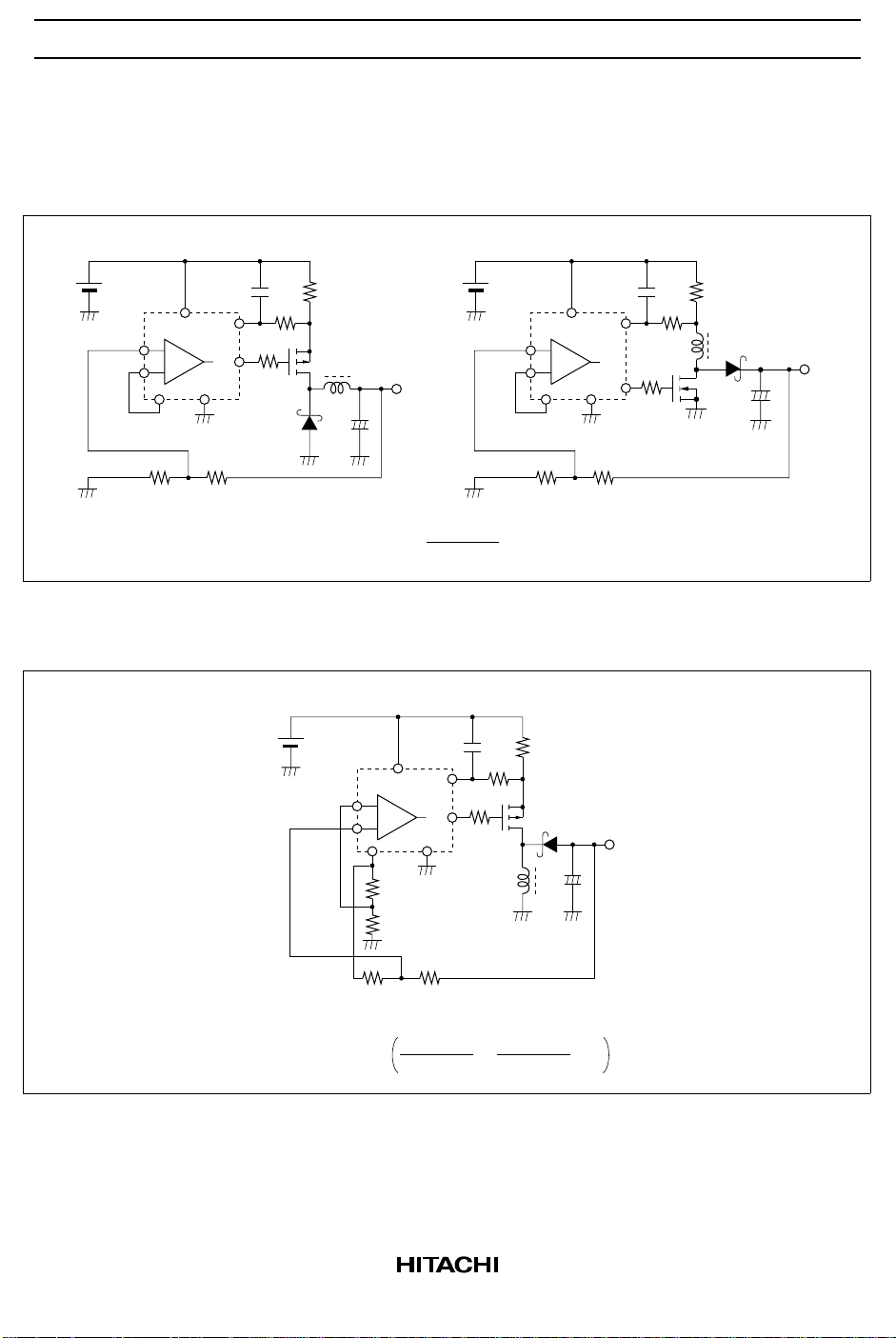
2. DC/DC Output Voltage Setting and Error Amplifier Usage
2.1 DC/DC Output Voltage Setting
(1) Positive Output Voltage (VO > Vref)
HA16114 with step-down topology HA16120 with step-down (boost) topology
C
IN(−)
IN(+)
V
IN
−
+
EA
GND
L
OUT
Vref
R
R
2
1
Figure 2.1 Output Voltage Setting (1)
(2) Negative Output Voltage (VO < 0 V)
HA16114 with inverting topology
IN(−)
IN(+)
V
O
+
−
V = VrefO×
V
IN
−
+
Vref
R
3
R
4
EA
C
IN(−)
IN(+)
V
IN
−
+
EA
GND
L
OUT
V
O
+
−
Vref
R
+ R
R
1
2
R
2
C
L
R
2
1
OUT
−
+
R
V = −VrefO×
2
R
1
R + R
12
R
2
R
×− 1
3
R + R
34
Figure 2.2 Output Voltage Setting (2)
9
Page 10
HA16114P/PJ/FP/FPJ, HA16120FP/FPJ
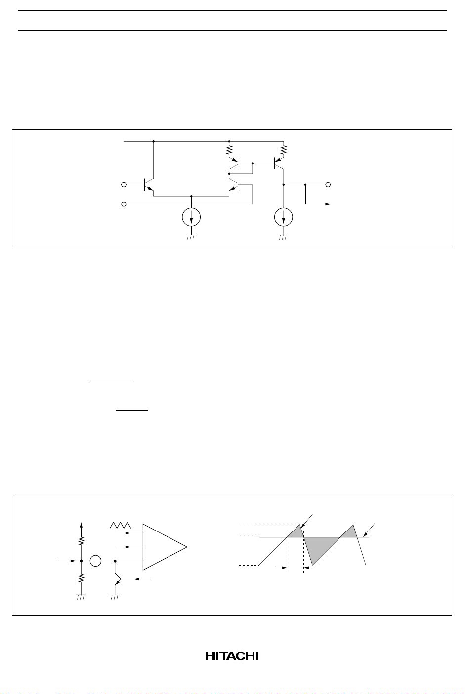
2.2 Error Amplifier Usage
Figure 2.3 shows an equivalent circuit of the error amplifier. The error amplifier in these ICs is a simple
NPN-transistor differential amplifier with a constant-current-driven output circuit.
The amplifier combines a wide bandwidth (fT = 4 MHz) with a low open-loop gain (50 dB Typ), allowing
stable feedback to be applied when the power supply is designed. Phase compensation is also easy.
IC internal V
IN(−)
IN(+)
IN
E/O
To internal PWM
comparator
µµ
40 A80 A
Figure 2.3 Error Amplifier Equivalent Circuit
3. Dead-Band Duty Cycle and Soft-Start Settings
3.1 Dead-Band Duty Cycle Setting
The dead-band duty cycle (the maximum duty cycle of the PWM pulse output) can be programmed by the
voltage VDB at the DB pin. A convenient way to obtain VDB is to divide the IC’s Vref output by two
external resistors. The dead-band duty cycle (DB) and VDB can be calculated as follows.
− V
V
TH
DB = ⋅ ⋅ ⋅ ⋅ This applies when VDB > VTL.
VTH − V
VDB = Vref ×
DB
TL
R
2
R1 + R
× 100 (%)
2
If V
< VTL, there is no PWM output.
DB
Note: VDB is the voltage at the DB pin.
VTH: 1.6 V (Typ)
VTL: 1.0 V (Typ)
Vref is typically 2.5 V. Select R1 and R2 so that 1.0 V ≤ VDB ≤ 1.6 V.
Sawtooth
DB
wave
E/O
PWM
COMP
−
+
+
from
UVL
V
TH
V
DB
V
TL
VTH and VTL vary depending on the oscillator.
Note:
Select constants by testing under implementation
conditions.
To Vref
R
1
V
DB
R
2
Figure 3.1 Dead-Band Duty Cycle Setting
10
Sawtooth wave
Dead band
Voltage at DB pin
Page 11
HA16114P/PJ/FP/FPJ, HA16120FP/FPJ
3.2 Soft-Start Setting
Soft-start avoids overshoot at power-up by widening the PWM output pulses gradually, so that the
converted DC output rises slowly. Soft-start is programmed by connecting a capacitor between the DB pin
and ground. The soft-start time is determined by the time constant of this capacitor and the resistors that
set the voltage at the DB pin.
V
t
= −C1 × R × ln (1 − )
soft
R
× R
1
R1 + R
2
2
R1 + R
R
2
R =
VDB = Vref ×
Note: VX is the voltage at the DB pin after time t (VX < VDB).
To Vref
R
V
X
1
Sawtooth
wave
E/O
DB
X
V
DB
2
Undervoltage
lockout released
1.6 V
V
PWM
COMP
−
+
+
TH
V
DB
V
TL
1.0 V
Sawtooth wave
C
R
1
2
from
UVL
V
X
UVL sink
transistor
t
Soft-start time
t
soft
Figure 3.2 Soft-Start Setting
3.3 Quick Shutdown
The quick shutdown function resets the voltages at all pins when the IC is turned off, to assure that PWM
pulse output stops quickly. Since the UVL pull-down resistor in the IC remains on even when the IC is
turned off, the sawtooth wave output, error amplifier output, and DB pin are all reset to low voltage.
This feature helps in particular to discharge capacitor C1 in figure 3.2, which has a comparatively large
capacitance. In intermittent mode (explained on a separate page), this feature enables the IC to soft-start in
each on-off cycle.
11
Page 12
HA16114P/PJ/FP/FPJ, HA16120FP/FPJ
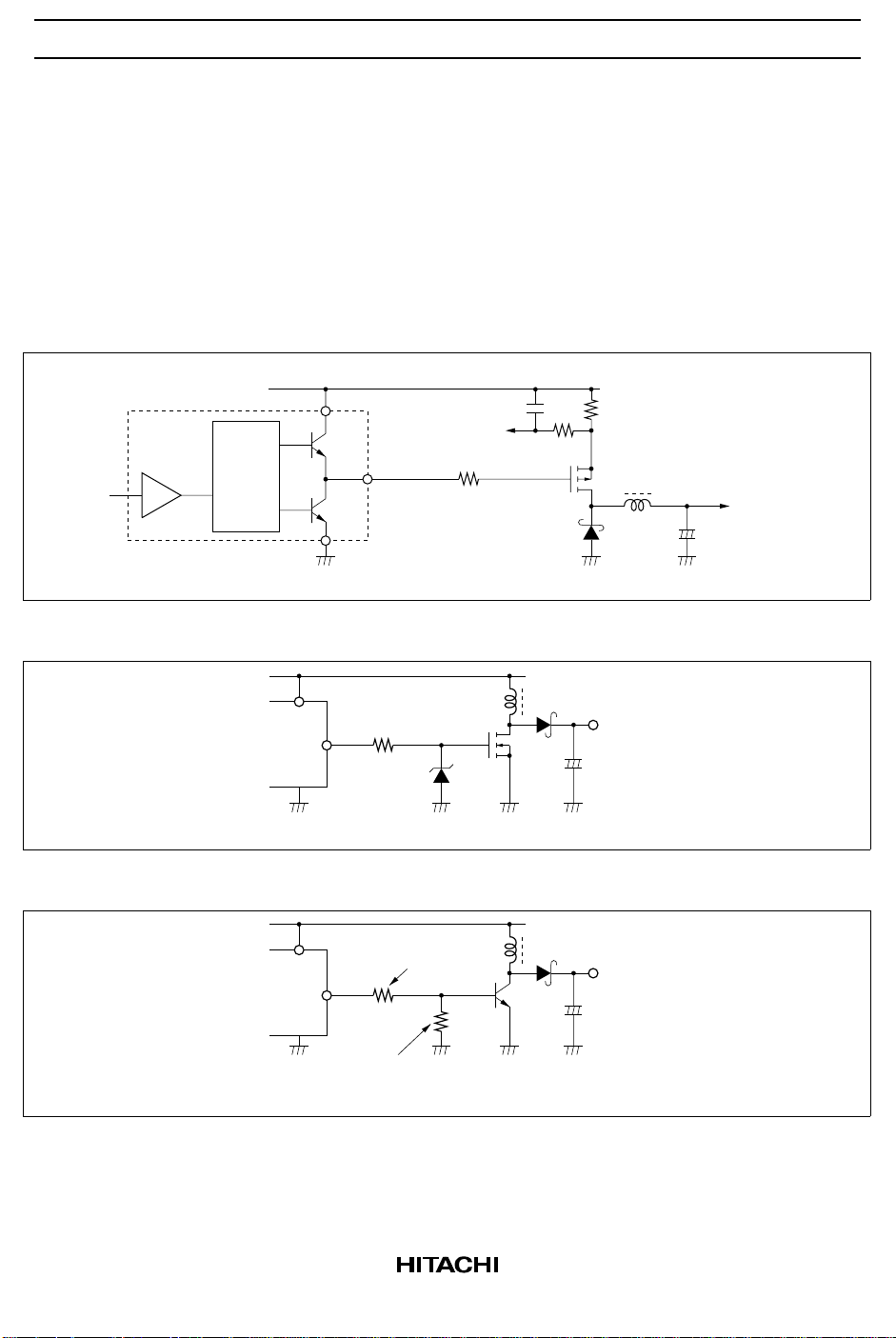
4. PWM Output Circuit and Power MOSFET Driving Method
These ICs have built-in totem-pole push-pull drive circuits that can drive a power MOS FET as shown in
figure 4.1. The power MOS FET can be driven directly through a gate protection resistor.
If VIN exceeds the gate breakdown voltage of the power MOS FET additional protective measures should
be taken, e.g. by adding Zener diodes as shown in figure 4.2.
To drive a bipolar power transistor, the base should be protected by voltage and current dividing resistors
as shown in figure 4.3.
V
IN
To C
Bias
circuit
Totem-pole output circuit
P.GND
OUT
Gate protection
resistor
L
R
G
Example:
P-channel power MOSFET
V
O
Figure 4.1 Connection of Output Stage to Power MOS FET
V
IN
R
G
V
O
OUT
GND
D
Z
Example: N-channel power MOSFET
Figure 4.2 Gate Protection by Zener Diodes
V
IN
Base current
limiting resistor
V
O
OUT
GND
Base discharging resistor
Example: NPN power transistor
Figure 4.3 Driving a Bipolar Power Transistor
12
Page 13

HA16114P/PJ/FP/FPJ, HA16120FP/FPJ
5. Voltage Reference (Vref = 2.5 V)
5.1 Voltage Reference
A bandgap reference built into the IC (see figure 5.1) outputs 2.5 V ± 50 mV. The sawtooth oscillator,
PWM comparator, latch, and other internal circuits are powered by this 2.5 V and an internally-generated
voltage of approximately 3.2 V.
The voltage reference section shut downs when the IC is turned off at the ON/OFF pin as described later,
saving current when the IC is not used and when it operates in intermittent mode during overcurrent.
V
ON/OFF
−
+
1.25 V
Sub bandgap circuit
Main bandgap circuit
1.25 V
25 kΩ
25 kΩ
IN
3.2 V
Vref
2.5 V
ADJ
Figure 5.1 Vref Reference Circuit
5.2 Trimming the Reference Voltage (Vref and ADJ pins)
Figure 5.2 shows a simplified circuit equivalent to figure 5.1. The ADJ pin in this circuit is provided for
trimming the reference voltage (Vref). The output at the ADJ pin is a voltage V
generated by the bandgap circuit. Vref is determined by V
and the ratio of internal resistors R1 and R2 as
ADJ
of 1.25 V (Typ)
ADJ
follows:
R
+ R
1
Vref = V
ADJ
×
2
R
2
The design values of R1 and R2 are 25 kΩ with a tolerance of ±25%.
If trimming is not performed, the ADJ pin open can be left open.
V
IN
Vref
ADJ
25 kΩ
R
1
(typ)
25 kΩ
R
2
(typ)
−
+
VBG (bandgap voltage)
1.25 V (typ)
Figure 5.2 Simplified Diagram of Voltage Reference Circuit
13
Page 14

HA16114P/PJ/FP/FPJ, HA16120FP/FPJ
The relation between Vref and the ADJ pin enables Vref to be trimmed by inserting one external resistor
(R3) between the Vref and ADJ pins and another (R4) between the ADJ pin and ground, to change the
resistance ratio. Vref is then determined by the combined resistance ratio of the internal R1 and R2 and
external R3 and R4.
R
+ R
A
Vref = V
ADJ
×
Where, RA: parallel resistance of R1 and R
RB: parallel resistance of R2 and R
Although Vref can be trimmed by R3 or R4 alone, to decrease the temperature dependence of Vref it is
better to use two resistors having identical temperature coefficients. Vref can be trimmed in the range of
2.5 V ± 0.2 V. Outside this range, the bandgap circuit will not operate and the IC may shut down.
External
resistors
B
R
B
3
4
Vref
R
3
ADJ
R
1
Internal
resistors
R
4
R
2
Figure 5.3 Trimming of Reference Voltage
RA =
RB =
R
1 R3
R1 + R
R
2 R4
R2 + R
3
4
5.3 Vref Undervoltage Lockout and Overvoltage Protection
The undervoltage lockout (UVL) function turns off PWM pulse output when the input voltage (VIN) is low.
In these ICs, this is done by monitoring the Vref voltage, which normally stays constant at approximately
2.5 V. The UVL circuit operates with hysteresis: it shuts PWM output off when Vref falls below 1.7 V,
and turns PWM output back on when Vref rises above 2.0 V. Undervoltage lockout also provides
protection in the event that Vref is shorted to ground.
The overvoltage protection circuit shuts PWM output off when Vref goes above 6.8 V. This provides
protection in case the Vref pin is shorted to VIN or another high-voltage source.
PWM
output
PWM
output
PWM output on
off
1.7 2.0 2.5 5.0 6.8
PWM output off
10
Vref
(V)
Figure 5.4 Vref Undervoltage Lockout and Overvoltage Protection
UVL Voltage Vref (V typ) VIN (V typ) Description
V
H
V
L
2.0 V 3.6 V VIN increasing: UVL releases; PWM output starts
1.7 V 3.3 V VIN decreasing: undervoltage lockout; PWM output stops
14
Page 15

HA16114P/PJ/FP/FPJ, HA16120FP/FPJ
6. Usage of ON/OFF Pin
This pin is used for the following purposes:
• To shut down the IC while its input power remains on (power management)
• To externally alter the UVL release voltage
• With the timer (TM) pin, to operate in intermittent mode during overcurrent (see next section)
6.1 Shutdown by ON/OFF Pin Control
The IC can be shut down safely by bringing the voltage at the ON/OFF pin below about 0.7 V (the internal
VBE value). This feature can be used in power supply systems to save power. When shut down, the
HA16114 draws a maximum current (I
ON/OFF pin sinks 290 µA (Typ) at 5 V, so it can be driven by TTL and other logic ICs. If intermittent
mode will also be employed, use a logic IC with an open-collector or open-drain output.
) of 10 µA, while the HA16120 draws a maximum 150 µA. The
OFF
External logic IC
Off On
Switch
C
ON/OFF
I
IN
R
A
R
B
TM
10 kΩ
+
−
ON/OFF
GND
To latch
3V
BE
V
IN
Q
Q
HA16114,
HA16120
1
2
V
IN
To other circuitry
Vref
reference
Q
3
On/off hysteresis circuit
Vref
output
Figure 6.1 Shutdown by ON/OFF Pin Control
6.2 Adjustment of UVL Voltages (when not using intermittent mode)
These ICs permit external adjustment of the undervoltage lockout voltages. The adjustment is made by
changing the undervoltage lockout thresholds VTH and VTL relative to VIN, using the relationships shown in
the accompanying diagrams.
When the IC is powered up, transistor Q3 is off, so VON is 2VBE, or about 1.4 V. Connection of resistors R
and RD in the diagram makes undervoltage lockout release at:
RC + R
V
IN
= 1.4 V ×
D
R
D
This VIN is the supply voltage at which undervoltage lockout is released. At the release point Vref is still
below 2.5 V. To obtain Vref = 2.5 V, VIN must be at least about 4.3 V.
C
Since V
operates in relation to the base-emitter voltage of internal transistors, VON has a temperature
ON/OFF
coefficient of approximately –4 mV/°C. Keep this in mind when designing the power supply unit.
When undervoltage lockout and intermittent mode are both used, the intermittent-mode time constant is
shortened, so the constants of external components may have to be altered.
15
Page 16

HA16114P/PJ/FP/FPJ, HA16120FP/FPJ
V
R
C
TM
(open)
To latch
ON/OFF
10 kΩ
R
D
3V
BE
GND
IN
Q
Q
2
I
IN
1
Vref
generation
circuit
Q
3
On/off hysteresis circuit
To other circuitry
Vref output
V
IN
3
2
2.5 V
V 4.5 V≥
IN
Vref
V
1
OFF
0.7 V
0
012345
V
ON
1.4 V
V
ON/OFF
Figure 6.2 Adjustment of UVL Voltages
7. Timing of Intermittent Mode during Overcurrent
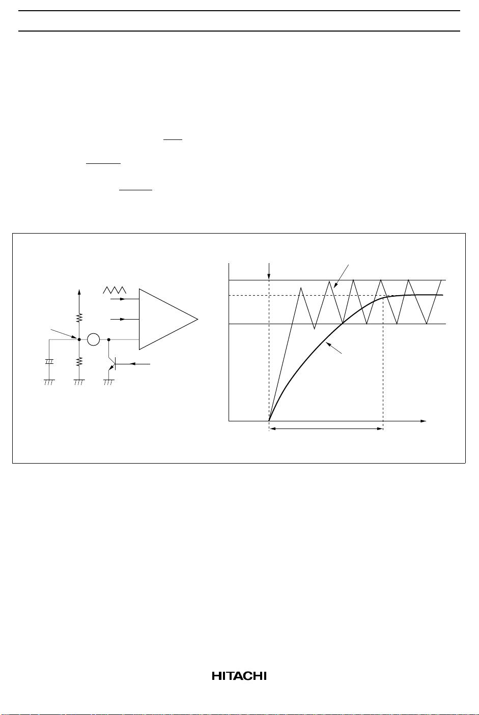
7.1 Principle of Operation
These ICs provide pulse-by-pulse overcurrent protection by sensing the current during each pulse and
shutting off the pulse if overcurrent is detected. In addition, the TM and ON/OFF pins can be used to
operate the IC in intermittent mode if the overcurrent state continues. A power supply with sharp settling
characteristics can be designed in this way.
Intermittent mode operates by making use of the hysteresis of the ON/OFF pin threshold voltages VON and
V
(VON – V
OFF
= VBE). The timing can be programmed as explained below.
OFF
When not using intermittent mode, leave the TM pin open, and pull the ON/OFF pin up to VON or higher.
The VBE is base emitter voltage of internal transistors.
16
V
IN
390 kΩ
2.2 kΩ
2.2 F
R
A
TM
R
B
ON/OFF
+
µ
C
ON/OFF
−
Vref
reference
Figure 7.1 Connection Diagram (example)
Latch
Q
S
R
Current
limiter
CL
Page 17

HA16114P/PJ/FP/FPJ, HA16120FP/FPJ
7.2 Intermittent Mode Timing Diagram (V
*1
3V
BE
2V
V
0 V
BE
IC is on
BE
V
ON/OFF
Continuous overcurrent is detected
a.
Intermittent operation starts (IC is off)
b.
Voltage if overcurrent ends (thick dotted line)
c.
Note: 1.
For details, see the overall waveform timing diagram.
V
is the base-emitter voltage of internal transistors, and is approximately 0.7 V.
BE
(See the figure 6.1.)
Figure 7.2 Intermittent Mode Timing Diagram (V
ON/OFF
2T
only)
a
ON
c
IC is off
c
On On
Off
b
T
ON
T
OFF
only)
ON/OFF
t
7.3 Calculation of Intermittent Mode Timing
Intermittent mode timing is calculated as follows.
(1) TON (time until the IC shuts off when continuous overcurrent occurs)
2V
T
= C
ON
= C
≈ 0.69 × C
(2) T
(time from when the IC shuts off until it next turns on)
OFF
T
= C
OFF
ON/OFF
ON/OFF
ON/OFF
× RB × ln
× RB × ln2 ×
× RB ×
ON/OFF
+ RB) × ln
× (R
A
BE
V
BE
1 − On duty*
1 − On duty*
VIN − 2V
Where VBE ≈ 0.7 V
×
1
1
VIN − V
1
1 − On duty*
BE
BE
The greater the overload, the sooner the pulse-by-pulse current limiter operates, the smaller tON becomes,
and from the first equation (1) above, the smaller TON becomes. From the second equation (2), T
OFF
depends on VIN. Note that with the connections shown in the diagram, when VIN is switched on the IC does
not turn on until T
has elapsed.
OFF
Sawtooth wave
PWM output
(In case of HA16114)
Note: On duty is the percent of time the IC output is on during one PWM cycle
when the pulse-by-pulse current limiter is operating.
t
ON
T
Dead-band voltage
Point at which the current
limiter operates
t
On duty = × 100 (%)
Where T = t/f
ON
T
OSC
Figure 7.3
17
Page 18

HA16114P/PJ/FP/FPJ, HA16120FP/FPJ
7.4 Examples of Intermittent Mode Timing (calculated values)
(1) T
ON
T = T C R
ON 1×ON/OFF×B
Here, coefficient
T = 0.691×
1 − On duty
from section 7.3 (1) previously.
Example: If C = 2.2 F,
ON/OFF
R = 2.2 k , and the on duty
B
of the current limiter is 75%,
then T = 13 ms.
Figure 7.4 Examples of Intermittent Mode Timing (1)
(2) T
OFF
T = T C (R + R )
OFF 2×ON/OFF
Here, coefficient
2
VIN − V
VIN − 2V
T = ln
from section 7.3 (2) previously.
×
BE
BE
1
ON
8
6
4
T
1
2
µ
Ω
0
0 20406080100
(PWM) On duty (%)
B
A
0.1
T
2
0.05
Example: Ωµ
If C = 2.2 F, R = 2.2 k ,
ON/OFF B
R = 390 k , V = 12 V,
AIN
T = 55 ms.
then
18
Ω
OFF
0
02040
10 30
V (V)
IN
Figure 7.5 Examples of Intermittent Mode Timing (2)
Page 19

HA16114P/PJ/FP/FPJ, HA16120FP/FPJ
Sawtooth wave V
Dead band V
Error output V
PWM pulse output
(In case of HA16120)
Power MOS FET
drain current (I
(dotted line shows
inductor current)
Current limiter
pin (CL)
DB
E/O
)
D
V
VIN − 0.2 V
CT
IN
V
Example of step-up circuit
V
IN
C
C
L
IC
OUT
Determined by L and V
TH
(CL)
Determined by RCS and R
F
R
CS
R
F
Inductor
L
V
OUT
F
F.B.
I
D
IN
Figure 7.6
8. Setting the Overcurrent Detection Threshold
The voltage drop VTH at which overcurrent is detected in these ICs is typically 0.2 V. The bias current is
typically 200 µA. The power MOS FET peak current value before the current limiter goes into operation is
given as follows.
VTH − (RF + RCS) × I
ID =
R
CS
BCL
Where, VTH = VIN – VCL = 0.2 V, VCL is a voltage refered on GND.
Note that RF and CF form a low-pass filter with a cutoff frequency determined by their RC time constant.
This filter prevents incorrect operation due to current spikes when the power MOS FET is switched on or
off.
V
IN
To other
circuitry
OUT
1 k
µ
200 A
Note: This circuit is an example for step-down use.
Detector
output
(internal)
IN(−)
CL
+−
Figure 8.1 Example for Step-Down Use
With the values shown in the diagram, the peak current is:
0.2 V − (240 Ω + 0.05 Ω) × 200 µA
ID =
0.05 Ω
= 3.04 A
The filter cutoff frequency is calculated as follows:
fC ==
1
2π C
F RF
6.28 × 1800 pF × 240 Ω
1
= 370 kHz
C
1800 pF
F
I
BCL
R
F
240 Ω
R
0.05 Ω
G
S
D
V
CS
IN
V
O
+
−
19
Page 20

HA16114P/PJ/FP/FPJ, HA16120FP/FPJ
Absolute Maximum Ratings (Ta = 25°C)
Rating
HA16114P/FP,
Item Symbol
Supply voltage V
Output current (DC) I
IN
O
HA16120FP
40 40 V
±0.1 ±0.1 A
Output current (peak) IO peak ±1.0 ±1.0 A
Current limiter input voltage V
Error amplifier input voltage V
E/O input voltage V
RT source current I
TM sink current I
SYNC voltage V
SYNC current I
Power dissipation P
CL
IEA
IE/O
RT
TM
SYNC
SYNC
T
V
IN
V
IN
Vref Vref V
500 500 µA
33mA
Vref Vref V
±250 ±250 µA
1, *2
680*
Operating temperature Topr –20 to +85 –40 to +85 °C
Junction temperature TjMax 125 125 °C
Storage temperature Tstg –55 to +125 –55 to +125 °C
Note: 1. This value is for an SOP package (FP) and is based on actual measurements on a 40 × 40 × 1.6
mm glass epoxy circuit board. With a 10% wiring density, this value is permissible up to Ta =
45°C and should be derated by 8.3 mW/°C at higher temperatures. With a 30% wiring density,
this value is permissible up to Ta = 64°C and should be derated by 11.1 mW/°C at higher
temperatures.
2. For the DILP package.
This value applies up to Ta = 45°C; at temperatures above this, 8.3 mW/°C derating should be
applied.
HA16114PJ/FPJ,
HA16120FPJ Unit
V
IN
V
IN
680*
1, *2
V
V
mW
20
800
T
600
400
200
Permissible dissipation P (mW)
680 mW
10% wiring density
30% wiring density
447 mW
348 mW
45°C64°C85°C 125°C
0
20 40 60 80 100 120 1400−20
Operating ambient temperature Ta (°C)
Page 21

HA16114P/PJ/FP/FPJ, HA16120FP/FPJ
Electrical Characteristics (Ta = 25°C, VIN = 12 V, f
= 100 kHz)
OSC
Item Symbol Min Typ Max Unit Test Conditions Notes
Voltage Output voltage Vref 2.45 2.50 2.55 V I
= 1 mA
O
reference Line regulation Line — 2 60 mV 4.5 V ≤ VIN ≤ 40V 1
section Load regulation Load — 30 60 mV 0 ≤ IO ≤ 10 mA
Short-circuit output
I
OS
10 24 — mA Vref = 0 V
current
Vref overvoltage
Vrovp 6.2 6.8 7.4 V
protection threshold
Temperature stability
∆Vref/∆Ta — 100 — ppm/°C
of output voltage
Vref adjustment
V
ADJ
1.225 1.25 1.275 V
voltage
Sawtooth Maximum frequency fmax 600 — — kHz
oscillator Minimum frequency fmin — — 1 Hz
section Frequency stability
with input voltage
Frequency stability
with temperature
Oscillator frequency f
Dead-band
adjustment
Low level threshold
voltage
section High level threshold
voltage
Threshold difference ∆V
∆f/f
∆f/f
OSC
V
V
01
02
— ±1 ±3 % 4.5 V ≤ VIN ≤ 40 V
= (fmax + fmin)/2)
(f
01
— ±5 — % –20°C ≤ Ta ≤ 85°C
(f
= (fmax + fmin)/2)
02
90 100 110 kHz RT = 10 kΩ
C
= 1300 pF
T
TL
0.9 1.0 1.1 V Output duty cycle:
0% on
TH
1.5 1.6 1.7 V Output duty cycle:
100% on
TH
0.5 0.6 0.7 V ∆VTH = VTH – V
TL
Output source current Isource 170 250 330 µA DB pin: 0 V
PWM
comparator
section High level threshold
Low level threshold
V
voltage
V
voltage
Threshold difference ∆V
TL
0.9 1.0 1.1 V Output duty cycle:
0% on
TH
1.5 1.6 1.7 V Output duty cycle:
100% on
TH
0.5 0.6 0.7 V ∆VTH = VTH – V
TL
Note: 1. Resistors connected to ON/OFF pin:
V pin
10
IN
Ω
390 k
12
TM pin
Ω
2 k
13
ON/OFF pin
21
Page 22

HA16114P/PJ/FP/FPJ, HA16120FP/FPJ
Electrical Characteristics (Ta = 25°C, VIN = 12 V, f
= 100 kHz) (cont)
OSC
Item Symbol Min Typ Max Unit
Error Input offset voltage V
amplifier Input bias current I
section Output sink current I
Output source
IO
B
Osink
I
Osource
— 2 10 mV
— 0.5 2.0 µA
28 40 52 µAVO = 2.5 V
28 40 52 µAVO = 1.0 V
current
Common-mode
V
CM
1.1 — 3.7 V
input voltage range
Voltage gain A
Unity gain
V
BW—4 —MHz
40 50 — dB f = 10 kHz
bandwidth
High level output
V
OH
3.5 4.0 — V IO = 10 µA
voltage
Low level output
V
OL
— 0.2 0.5 V IO = 10 µA
voltage
Overcurrent Threshold voltage V
detection CL(–) bias current I
section Turn-off time t
TH
BCL(–)
OFF
VIN –0.22 VIN –0.2 VIN –0.18 V
140 200 260 µA CL(–) = V
— 200 300 ns 1
500 600 2
UVL section Vref high level
V
TH
1.7 2.0 2.3 V
threshold voltage
Vref low level
V
TL
1.4 1.7 2.0 V
threshold voltage
Threshold
∆
VTH
0.1 0.3 0.5 V ∆VTH = VTH – V
difference
VIN high level
V
INH
3.3 3.6 3.9 V
threshold voltage
VIN low level
V
INL
3.0 3.3 3.6 V
threshold voltage
Notes: 1. HA16114 only.
2. HA16120 only.
Test
Conditions Notes
IN
TL
22
Page 23

HA16114P/PJ/FP/FPJ, HA16120FP/FPJ
Electrical Characteristics (Ta = 25°C, VIN = 12 V, f
Item
Symbol Min Typ Max Unit
Output Output low voltage V
stage Output high voltage V
High voltage when off V
Low voltage when off V
Rise time t
Fall time t
External
sync
SYNC source
current
section Sync input
frequency range
External sync
initiation voltage
Minimum pulse
width of sync input
Input sync pulse
duty cycle
On/off
section
ON/OFF sink
current 1
ON/OFF sink
current 2
IC on threshold V
IC off threshold V
ON/OFF threshold
difference
Total Operating current I
device Quiescent current I
Notes: 1. HA16114 only.
2. HA16120 only.
3. PW = t
/ t2 × 100
1
External
sync pulse
t
1
OL
OH1
OH2
OL2
r
f
I
SYNC
f
SYNC
V
SYNC
PWmin 300 — — ns
PW 5 — 50 % 3
I
ON/ OFF 1
I
ON/ OFF 2
ON
OFF
∆V
IN
OFF
t
2
— 0.9 1.5 V I
VIN –2.2 VIN –1.6 — V I
VIN –2.2 VIN –1.6 — V I
— 0.9 1.5 V I
— 50 200 ns CL = 1000 pF
— 50 200 ns CL = 1000 pF
120 180 240 µA SYNC pin: 0 V
f
OSC
—f
Vref –1.0 — Vref –0.5 V
60 90 120 µA ON/OFF pin: 3 V
220 290 380 µA ON/OFF pin: 5 V
1.1 1.4 1.7 V
0.4 0.7 1.0 V
0.5 0.7 0.9 V
ON/OFF
6.0 8.5 11.0 mA CL = 1000 pF
0—10µA ON/OFF pin: 0 V 1
— 120 150 µA ON/OFF pin: 0 V 2
= 100 kHz) (cont)
OSC
× 2 kHz
OSC
Test Conditions
= 10 mA
Osink
= 10 mA
Osource
= 1 mA
Osource
ON/OFF pin: 0 V
= 1 mA
Osink
ON/OFF pin: 0 V
Notes
1
2
23
Page 24

HA16114P/PJ/FP/FPJ, HA16120FP/FPJ
Characteristic Curves
Reference Voltage vs. Supply Voltage Reference Voltage vs. Ambient Temperature
4.0
Ta = 25°C
2.54
V = 12 V
IN
2.55 max
3.0
2.5V
2.0
1.0
Reference voltage (V)
0.0
01234
4.3V
540
Supply voltage (V)
Low Level Threshold Voltage of Sawtooth Wave vs.
Frequency
2.5
Ta = 25°C
V = 12 V
IN
2.0
R = 10 k
T
Ω
1.5
2.52
2.50
SPEC
2.48
Reference voltage (V)
2.45 min
2.46
−20
0 20406080
Ambient temperature (°C)
High Level Threshold Voltage of Sawtooth Wave vs.
Frequency
2.5
Ta = 25°C
V = 12 V
IN
2.0
R = 10 k
T
Ω
1.5
1.0
sawtooth wave (V)
0.5
Low level threshold voltage of
0.0
100 200 300 400 500 600
Frequency (kHz)
24
1.0
sawtooth wave (V)
0.5
High level threshold voltage of
0.0
100 200 300 400 500 600
Frequency (kHz)
Page 25

HA16114P/PJ/FP/FPJ, HA16120FP/FPJ
Oscillator Frequency Change
with Ambient Temperature (1)
10
V = 12 V
IN
f = 100 kHz
OSC
5
0
−5
Oscillator frequency change (%)
−10
−20
0 20406080
Ambient temperature (°C)
Error Amplifier Gain, Error Amplifier Phase vs. Error Amplifier Input Frequency
60
(dB)
VO
40
Oscillator Frequency Change
with Ambient Temperature (2)
10
V = 12 V
IN
f = 350 kHz
OSC
5
SPEC
0
−5
Oscillator frequency change (%)
−10
−20
0 20406080
Ambient temperature (°C)
A
VO
0
φ
20
Error amplifier gain A
0
1 k 3 k 10 k 30 k 100 k
Error amplifier input frequency fIN (Hz)
BW
300 k 1 M 3 M 10 M
45
90
135
180
Error amplifier phase φ (deg.)
25
Page 26

HA16114P/PJ/FP/FPJ, HA16120FP/FPJ
Error Amplifier Voltage Gain vs. Ambient Temperature
60
V = 12 V
IN
f = 10 kHz
55
50
50 dB typ
45
Error amplifier voltage gain (dB)
40 dB min
40
−20
0 20406080
Ambient temperature (°C)
Current Limiter Threshold Voltage vs.
0.22
V = 12 V
Ambient Temperature
IN
0.22 max
Current Limiter Turn-Off Time vs.
Current Limiter Threshold Voltage
500
• HA16114
400
300
Ta = 25°C
V = 12 V
IN
C = 1000 pF
L
300 ns max
200
Current limiter turn-off time (ns)
100
0.1 0.2 0.3 0.4 0.5
CL voltage VIN−VCL (V)
Note: Approximatery 300 ns greater than this
in the case of the HA16120.
Current Limiter Turn-Off Time vs.
300
Ambient Temperature
• HA16114
300 ns max
Note
Note
0.21
0.20
0.19
Current limiter threshold voltage (V)
0.18
−20
0 20406080
0.18 min
Ambient temperature (°C)
250
200
200 ns typ
V = 12 V
IN
V = V − 0.3 V
150
CL
C = 1000 pF
TH
L
Current limiter turn-off time (ns)
100
−20
0 20406080
Ambient temperature (°C)
Note: Approximatery 300 ns greater than this
in the case of the HA16120.
26
Page 27

HA16114P/PJ/FP/FPJ, HA16120FP/FPJ
Reference Voltage vs. IC On/Off Voltages IC On/Off Voltages vs. Ambient Temperature
5.0
Ta = 25°C
V = 12 V
IN
4.0
IC off voltage
3.0
SPEC SPEC
2.0
Reference voltage (V)
1.0
IC on voltage
2.0
1.5
1.0
IC on/off voltage (V)
0.5
V = 12 V
IN
f = 100 kHz
OSC
SPEC
IC on voltage
SPEC
IC off voltage
0.0
0 0.5 1.0 1.5 2.0 2.5
IC on/off voltage (V)
600
Ta = 25°C
V = 12 V
IN
500
f = 100 kHz
OSC
400
300
200
Peak output current (mA)
100
0
0 1000 2000 3000 4000 5000
Load capacitance (pF)
0.0
−20
0 20406080
Ambient temperature (°C)
Operating Current vs. Supply VoltagePeak Output Current vs. Load Capacitance
20
Ta = 25°C
f = 100 kHz
OSC
On duty = 50%
15
C = 1000 pF
L
SPEC
10
5
Operating current (mA)
0
010203040
Supply voltage (V)
27
Page 28

HA16114P/PJ/FP/FPJ, HA16120FP/FPJ
Operating Current vs. Output Duty Cycle
20
Ta = 25°C
V = 12 V
IN
f = 100 kHz
OSC
15
C = 1000 pF
L
SPEC
10
5
Operating current (mA)
0
0 20 40 80 10060
Output duty cycle (%)
PWM Comparator Input vs. Output Duty Cycle (1)
100
• HA16114
80
60
40
ON duty (%)
f
OSC
600 kHz
50 kHz
20
300 kHz
0
0.6 1.61.41.21.00.8 1.8
VDB or V
E/O
(V)
Note: The on-duty of the HA16114 is the proportion
of one cycle during which output is low.
PWM Comparator Input vs. Output Duty Cycle (2)
100
• HA16120
80
60
f
OSC
600 kHz
40
ON duty (%)
20
0
0.6 1.61.41.21.00.8 1.8
300 kHz
VDB or V
50 kHz
(V)
E/O
Note: The on-duty of the HA16120 is the proportion
of one cycle during which output is high.
28
Page 29

HA16114P/PJ/FP/FPJ, HA16120FP/FPJ
Output pin (Output Resistor) Characteristics
12
• HA16114
11
)
10
DC
(V
9
O
• HA16120
3
2
Output voltage V
1
0
024 8106
Io sink or Io source (mA)
Output high voltage
when on
Output high voltage
when off
Output low voltage
when on
Output low voltage
when off
VGS
(P-channel
Power MOS FET)
VGS
(N-channel
Power MOS FET)
29
Page 30

HA16114P/PJ/FP/FPJ, HA16120FP/FPJ
V
OUT
(V)
I
O
(mA)
15
10
400
200
−200
−400
15
Output Waveforms: Rise of Output Voltage V
OUT
5
0
Vref DB CL(−)V
IN
OUT
C
L
I
1000 pF
O
IN(+) C
R
T
10 kΩ
T
1300 pF
0
Test Circuit
200 ns/div
Output Waveforms: Fall of Output Voltage V
OUT
V
OUT
(V)
I
O
(mA)
10
400
200
−200
−400
5
0
Vref DB CL(−)V
IN
OUT
C
L
I
1000 pF
O
IN(+) C
R
T
10 kΩ
T
1300 pF
0
Test Circuit
200 ns/div
30
Page 31

OSC
1000
100
10
HA16114P/PJ/FP/FPJ, HA16120FP/FPJ
Oscillator Frequency vs. Timing Capacitance
RT = 3kΩ
RT = 10kΩ
RT = 30kΩ
Oscillator frequency f (kHz)
RT = 300kΩ
RT = 1MΩ
1
RT = 100kΩ
0.1
10
1
10
2
Timing capacitance C (pF)
10
3
10
4
T
10
5
10
6
31
Page 32

HA16114P/PJ/FP/FPJ, HA16120FP/FPJ
Application Examples (1)
High-saturation-current choke coil
Example: Toko 8R-HB Series
Low on-resistance
P-channel power MOSFET
Example: 2SJ214, 2SJ296
2
GDS
1
Overcurrent sense resistor
50m
220
+
1800p
−
5D
5.6
+
stepped-
down
output
4
560µ
Low-ESR
47µH
12V
capacitor 5 V DC
+
−
3
SBD
HRP24
0.22 µ
(noise-
absorbing
capacitor)
(gate protection resistor)
OUT
IN
IN(−) E/O IN(+) P.GND
T
C
HA16114FP
ON/OFF TM CL(−)V
T
−
5A
Power ground
470p
5k 5k
130k
560p
Units: C : F
Feedback
R : Ω
Separate the power ground from the small-signal ground,
and connect both at one point.
Add noise-absorbing capacitors.
Ground the bottom of the package with a ground strip.
Make the output-to-gate wiring as short as possible.
Noise countermeasures:
5A
5B
5C
5D
.
F
2µ
2 k
390 k
Step-Down Converter Using HA16114FP
DC
Timing circuit for
intermittent mode
during overcurrent
to 5 V
DC
− +
4.7µ
Dead-band and
soft-start circuit
• 12 V
32
15 k 10 k
+
16 13 12 11 10 915 14
Vref ADJ DB
0.1µ
5B
470 µ
−
+
12 V DCinput
35 V
(noise-
−
1 4567823
GND SYNC R
5C
absorbing
capacitor)
10k
Ground strip
Small-signal ground
5A
Use a switching element (power MOS FET) with low on-resistance.
Specific tips for high efficiency (see the numbers in the diagram)
1 5
Use a low-ESR capacitor designed for switching power supplies.
Use an inductor with low DC resistance.
Use a Schottky barrier diode (SBD) with low V
234
Page 33

HA16114P/PJ/FP/FPJ, HA16120FP/FPJ
Application Examples (2)
• External Synchronization with Primary-Control AC/DC Converter
(1) Combination with a flyback AC/DC converter (simplified schematic)
HRA83
Commercial AC
+
−
Error amp.
−
+
CL(CS)
Primary AC/DC converter IC
(HA16107, HA17384, etc.)
V
IN
OUT
1S2076A
+
Transformer
1S2076A
Step-down
output
(HA16114)
D
R
1
R
2
2
SYNC
HRP24
SBD
HA16114,
HA16120
P.GNDOUTGND
To A of SBD
891
+
−
V
IN
CL
K
A
HRP24
10
11
2SJ296
SBD
+
Main DC
output
−
+
Sub DC
−
output
+
−
This is one example of a circuit that uses the features of the HA16114/120 by operating in
synchronization with a flyback AC/DC converter. Note the following design points concerning the
circuit from the secondary side of the transformer to the SYNC pin of the HA16114/120.
• Diode D prevents reverse current. Always insert a diode here. Use a general-purpose switching
diode.
• Resistors R
does not exceed Vref (2.5 V). To maintain operating speed, R
and R2 form a voltage divider to ensure that the input voltage swing at the SYNC pin
1
+ R2 should not exceed 10 kΩ.
1
33
Page 34

HA16114P/PJ/FP/FPJ, HA16120FP/FPJ
Application Examples (3)
• External Synchronization with Primary-Control AC/DC Converter (cont.)
(2) Combination with a forward AC/DC converter (simplified schematic)
DFG1C8
D
HRW26F
HA17431 and optocoupler
Input
C
A
B
SBD
module
Feedback
section
+
Main DC
output
−
HA16107,
HA16666 etc.
Switching transformer
A
Coil
Coil
Coil
Coil
Primary, for main
B
Secondary, for output
Tertiary, for IC
C
D
For reset
2SC458
390Ω
R
3
R
6.2kΩ
1
SYNC V
Q
R
510Ω
2
ZD
FB
V
IN
210
HA16114,
HA16120
GND
1
IN
OUT
9
Other parts as
on previous page
This circuit illustrates the combination of the HA16114/120 with a forward AC/DC converter. The
HA16114/120 synchronizes with the falling edge of the external sync signal, so with a forward
transformer, the sync pulses must be inverted. In the diagram, this is done by an external circuit
consisting of the following components:
34
• Q:
• R
• R
• ZD:
and R2:
1
:
3
Transistor for inverting the pulses. Use a small-signal transistor.
These resistors form a voltage divider for driving the base of transistor Q. R
a path for base discharge, so that the transistor can turn off quickly.
Load resistor for transistor Q.
Zener diode for protecting the SYNC pin.
also provides
2
Page 35

HA16114P/PJ/FP/FPJ, HA16120FP/FPJ
Overall Waveform Timing Diagram (for Application Example (1))
12 V
V
IN
0 V
V ,
E/O
TM
V
ON/
OFF
1.4 V
0.7 V
On
On
On
On
On
OffOffOffOff
V ,
V
V
E/O
V ,
CT
V
DB
TM
ON/OFF
,
0.0 V
1.4 V
(V)
3.0
2.0
1.0
2.1 V
V
sawtooth wave
V
CT
Off
V
DB
0.0
12 V
V
CL
11.8 V
0 V
Pulse-by-pulse
current limiting
12 V
*1
V
OUT
PWM
pulse
0 V
DC/DC output
(example for
positive
voltage)
Soft start Steady state Overcurrent
IC operation
status
detected;
intermittent
operation
Power-up IC on
Note: 1. This PWM pulse is on the step-down/inverting control channel (HA16114).
The booster control channel (HA16120) output consists of alternating L and H of the IC on cycle.
Overcurrent
subsides;
steady-state
operation
Power supply off,
IC off
Quick
shutdown
35
Page 36

HA16114P/PJ/FP/FPJ, HA16120FP/FPJ
Application Examples (4) (Some Pointers on Use)
1. Inductor, Power MOS FET, and Diode Connections
1. Step-up topology 2. Step-down topology
V
IN
C
F
V
IN
R
Applicable only
CS
R
F
to HA16120
CL
V
OUT
GND
FB
V
IN
C
V
IN
CL
OUT
O
GND
4. Step-down/step-up (buck-boost) topology3. Inverting topology
F
R
Applicable only
R
CS
F
to HA16114
V
O
FB
C
F
V
IN
R
Applicable only
R
CS
F
to HA16114
CL
OUT
GND
FB
Vref
2. Turning Output On and Off while the IC is On
To turn only one channel off, ground the DB pin or the E/O pin.
In the case of E/O, however, there will be no soft start
when the output is turned back on.
V
DB
E/O
C
F
V
IN
R
Applicable only
R
CS
F
to HA16114
CL
OUT
O
GND
FB
OFF
36
Page 37

Package Dimensions
HA16114P/PJ/FP/FPJ, HA16120FP/FPJ
19.20
20.00 Max
16 9
1.3
1.11 Max
2.54 ± 0.25
81
0.48 ± 0.10
6.30
7.40 Max
5.06 Max
2.54 Min
0.51 Min
0° – 15°
Hitachi Code
JEDEC
EIAJ
Mass
(reference value)
0.25
7.62
+ 0.13
– 0.05
Unit: mm
DP-16
Conforms
Conforms
1.07 g
10.06
10.5 Max
16
1
0.80 Max
1.27
*0.42 ± 0.08
± 0.06
0.40
*Dimension including the plating thickness
Base material dimension
9
8
0.12
5.5
0.10 ± 0.10
0.15
M
2.20 Max
7.80
0.20 ± 0.04
*0.22 ± 0.05
0.70 ± 0.20
Hitachi Code
JEDEC
EIAJ
(reference value)
Mass
+ 0.20
– 0.30
1.15
0
° – 8°
FP-16DA
—
Conforms
0.24 g
Unit: mm
37
Page 38

HA16114P/PJ/FP/FPJ, HA16120FP/FPJ
Cautions
1. Hitachi neither warrants nor grants licenses of any rights of Hitachi’s or any third party’s patent,
copyright, trademark, or other intellectual property rights for information contained in this document.
Hitachi bears no responsibility for problems that may arise with third party’s rights, including
intellectual property rights, in connection with use of the information contained in this document.
2. Products and product specifications may be subject to change without notice. Confirm that you have
received the latest product standards or specifications before final design, purchase or use.
3. Hitachi makes every attempt to ensure that its products are of high quality and reliability. However,
contact Hitachi’s sales office before using the product in an application that demands especially high
quality and reliability or where its failure or malfunction may directly threaten human life or cause risk
of bodily injury, such as aerospace, aeronautics, nuclear power, combustion control, transportation,
traffic, safety equipment or medical equipment for life support.
4. Design your application so that the product is used within the ranges guaranteed by Hitachi particularly
for maximum rating, operating supply voltage range, heat radiation characteristics, installation
conditions and other characteristics. Hitachi bears no responsibility for failure or damage when used
beyond the guaranteed ranges. Even within the guaranteed ranges, consider normally foreseeable
failure rates or failure modes in semiconductor devices and employ systemic measures such as failsafes, so that the equipment incorporating Hitachi product does not cause bodily injury, fire or other
consequential damage due to operation of the Hitachi product.
5. This product is not designed to be radiation resistant.
6. No one is permitted to reproduce or duplicate, in any form, the whole or part of this document without
written approval from Hitachi.
7. Contact Hitachi’s sales office for any questions regarding this document or Hitachi semiconductor
products.
Hitachi, Ltd.
Semiconductor & Integrated Circuits.
Nippon Bldg., 2-6-2, Ohte-machi, Chiyoda-ku, Tokyo 100-0004, Japan
Tel: Tokyo (03) 3270-2111 Fax: (03) 3270-5109
URL NorthAmerica : http:semiconductor.hitachi.com/
For further information write to:
Hitachi Semiconductor
(America) Inc.
179 East Tasman Drive,
San Jose,CA 95134
Tel: <1> (408) 433-1990
Fax: <1>(408) 433-0223
Europe : http://www.hitachi-eu.com/hel/ecg
Asia (Singapore) : http://www.has.hitachi.com.sg/grp3/sicd/index.htm
Asia (Taiwan) : http://www.hitachi.com.tw/E/Product/SICD_Frame.htm
Asia (HongKong) : http://www.hitachi.com.hk/eng/bo/grp3/index.htm
Japan : http://www.hitachi.co.jp/Sicd/indx.htm
Hitachi Europe GmbH
Electronic components Group
Dornacher Straβe 3
D-85622 Feldkirchen, Munich
Germany
Tel: <49> (89) 9 9180-0
Fax: <49> (89) 9 29 30 00
Hitachi Europe Ltd.
Electronic Components Group.
Whitebrook Park
Lower Cookham Road
Maidenhead
Berkshire SL6 8YA, United Kingdom
Tel: <44> (1628) 585000
Fax: <44> (1628) 778322
Hitachi Asia Pte. Ltd.
16 Collyer Quay #20-00
Hitachi Tower
Singapore 049318
Tel: 535-2100
Fax: 535-1533
Hitachi Asia Ltd.
Taipei Branch Office
3F, Hung Kuo Building. No.167,
Tun-Hwa North Road, Taipei (105)
Tel: <886> (2) 2718-3666
Fax: <886> (2) 2718-8180
Copyright ' Hitachi, Ltd., 1998. All rights reserved. Printed in Japan.
38
Hitachi Asia (Hong Kong) Ltd.
Group III (Electronic Components)
7/F., North Tower, World Finance Centre,
Harbour City, Canton Road, Tsim Sha Tsui,
Kowloon, Hong Kong
Tel: <852> (2) 735 9218
Fax: <852> (2) 730 0281
Telex: 40815 HITEC HX
 Loading...