

Page 1

HA16113FPJ
Dual Watchdog Timers
The HA16113FPJ is a multifunction device that provides microprocessor systems with the necessary
regulated power supply, monitors the supply voltage, and generates power-on reset and watchdog reset
signals. It is ideally suited for battery-operated systems such as instrumentation systems.
Functions
• Regulated power supply
• Power-on reset
• Two built-in auto-reset circuits
• Two built-in watchdog timer circuits (WDT)
• Output voltage monitoring (LVI)
Features
• Simultaneous or independent control of auto-reset outputs.
• Precisely regulated output voltage and accurate NMI trigger voltage (both ±2%).
• Low-voltage control with NMI, simultaneous RES1 and RES2, and STBY outputs.
• Independently selectable durations for power-on reset and auto-reset: power-on duration is common to
both reset outputs; auto-reset durations can be selected independently.
• Reset command input pin (CONT) for second reset output (RES2).
• WDT filter function detects minimum pulse width and maximum period of P-RUN input pulses.
Page 2
HA16113FPJ
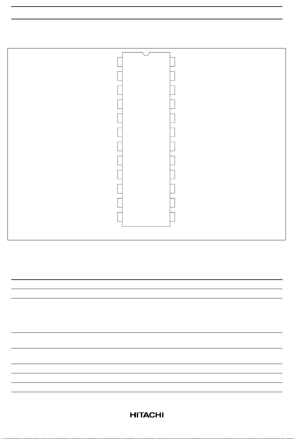
Pin Arrangement
P-RUN1
Cf1
Rf
C
R1
STBYadj
STBY
RES1
NMI
NMIadj
Re1
Re2
GND
1
2
3
4
5
6
7
8
9
10
11
12
(Top view)
24
23
22
21
20
19
18
17
16
15
14
13
P-RUN2
Cf2
R
R
C
R2
SW
CONT
RES2
C
RES
V
OUT
V
CONT
CS
V
CC
Pin Description
Pin No. Symbol Function
1 P-RUN1 Input from main CPU to watchdog timer 1 (WDT1)
2 Cf1 For connecting capacitor Cf1 to determine WDT1 filter characteristic (frequency band)
3 Rf For connecting common bias resistor Rf to determine WDT1 and WDT2 filter
4CR1For connecting capacitor CR1 to determine ton for power-on reset and t
5 STBY adj For adjusting standby trigger voltage (insert a resistor between this pin and ground)
6 STBY Standby signal output
7 RES1 Reset signal output to main CPU
8 NMI Low-voltage interrupt signal output for memory backup
2
characteristics (frequency band), power-on reset time (t
RES2), clock-off time of auto-reset circuits 1 and 2, reset high time (t
low time (t
resistor value from 100 kΩ to 500 kΩ.
RL1
and t
), and reset pulse delay at voltage drop and recovery. Use the
RL2
, common to RES1 and
on
of auto-reset circuit 1.
Recommended range: V
= 2.8 to 4.0 V
H2
RH1
off1
and t
, t
RH1
),reset
RH2
, and t
RL1
Page 3

HA16113FPJ
Pin Description (cont)
Pin No. Symbol Function
9 NMI adj For fine adjustment of Vout trigger level for NMI signal (insert a resistor between this
10 Re1 For connecting resistor Re1 to determine voltage Vout for microprocessor and IC
11 Re2 For connecting resistor Re2 to determine voltage Vout for microprocessor and IC
12 GND Ground
13 V
CC
14 CS Input for detecting power supply current
15 V
C
16 Vout Regulated voltage supplied to microprocessor and IC internal circuits Connect to
17 C
RES
18 RES2 Reset signal output to sub CPU
19 CONT Input pin for resetting sub CPU on command, or when sub CPU crashes Low input at
20 SW Selects simultaneous control, in which main and sub CPUs are both reset when main
21 C
22 R
R2
R
23 Cf2 For connecting capacitor Cf2 to determine WDT2 filter characteristic (frequency band)
24 P-RUN2 Input from sub CPU to watchdog timer 2 (WDT2)
pin and Vout or ground)
Recommended range: V
= 4.4 to 5.2 V
H1
internal circuits (insert between this pin and Re2)
internal circuits (insert between this pin and ground)
Power supply input pin (operating range: 6 to 40 V)
For base control of external pnp transistor
collector of external pnp transistor
Determines reset pulse delay at voltage drop and recovery. NMI output goes low as
soon as Vout drops below NMI trigger level. If Vout remains below this level for time
t
, both reset outputs also go low. When Vout recovers above NMI trigger level, first
RES
NMI output goes high, then after time t
t
are adjusted by capacitor C
r
RES
both reset outputs also go high. Times t
r
inserted between this pin and ground.
RES
CONT causes low output at RES2
CPU crashes, or independent control, in which sub CPU is reset independently of
main CPU
Open—independent control; connected to ground—simultaneous control
For connecting capacitor CR2 to determine t
For connecting bias resistor RR to determine t
resistor value from 100 kΩ to 500 kΩ.
off2
, t
off1
RH2
, t
, and t
off2
of auto-reset circuit 2
RL2
, t
, t
, t
RH1
RH2
RL1
, and t
. Use the
RL2
and
3
Page 4
HA16113FPJ
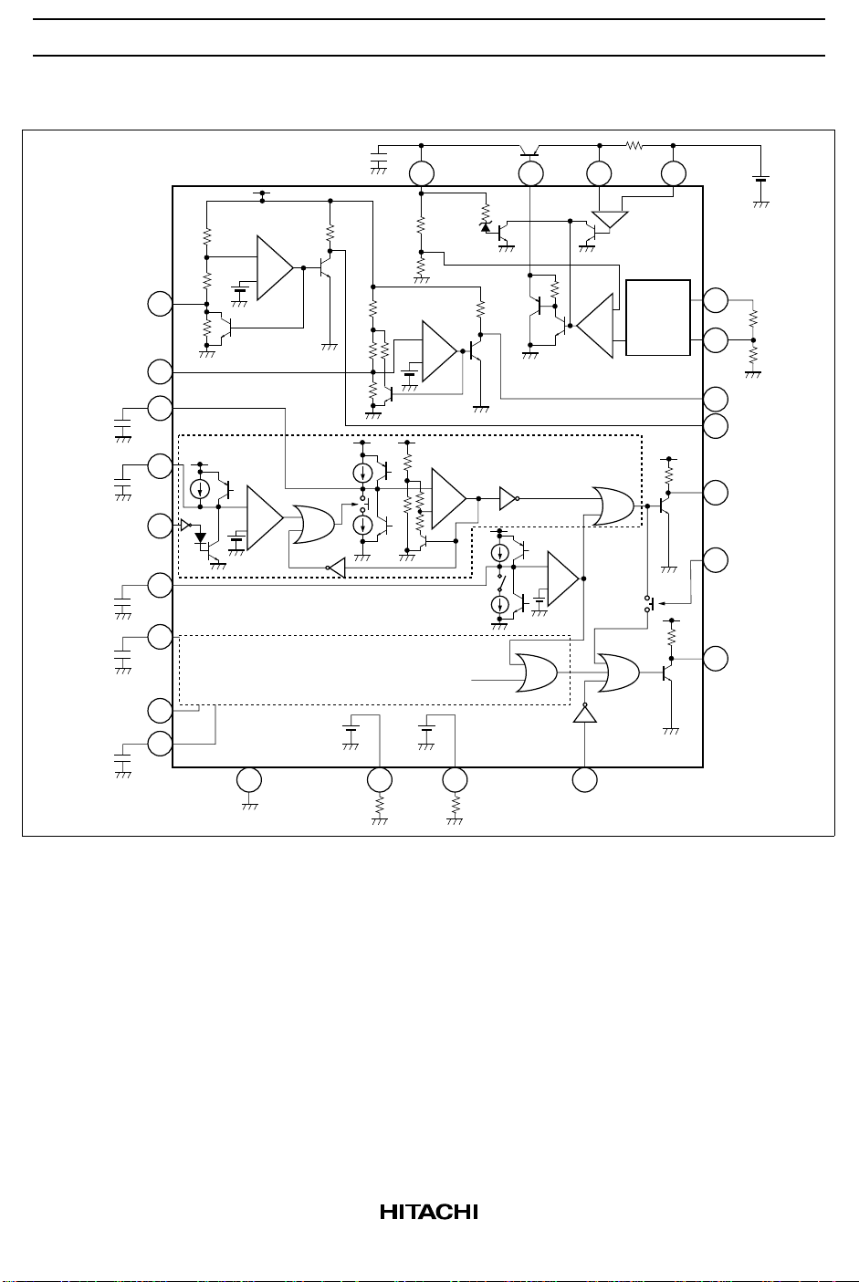
Block Diagram
STBY
adj
5
NMI
adj
9
C
R1
4
2
Cf1
1
P-RUN1
C
RES
17
C
R2
21
36.8 k
I/6
STBYdetection
block
71 k
—
31.2 k
+
19*I
—
+
16 15 14 13
3.3 k
NMI detection
block
2 k
80 k
69.7k
25 k
19 k
I
8.4 k
33 k
I*4/3
Delay circuit block
Auto-reset circuit 2
V
OUT
Over
voltage
detection
block
—
+
+
—
20 k
V
CONT
3.3 k
Regulator block
Auto-reset circuit 1
+
—
CS
Reference
—
+
Detection
block
voltage
circuit
3.3 k
3.3 k
V
CC
10
Re2
11
8
6
RES1
7
20
SW
RES2
18
Re1
NMI
STBY
P-RUN2
Cf2
24
23
I
1
RfGND
I
2
1922312
R
CONTR
4
Page 5
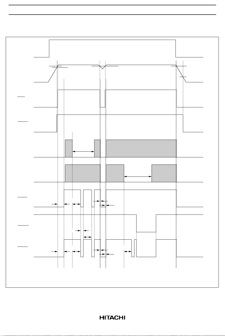
Timing Waveforms
V
BATT
HA16113FPJ
Vout
NMI
STBY
P-RUN1
P-RUN2
RES1
4.7 V
t
on
4.5 V
t
OFF1
4.6 V 4.7 V
Crash
t
RES
4.6 V (V )
NMI
3.0 V (V )
STBY
Crash
t
r
CONT
RES2
t
on
t
RL1
t
OFF1
Note: SW pin is connected to ground.
t
RH1
t
RES
t
OFF2
t
r
5
Page 6

HA16113FPJ
Absolute Maximum Ratings (Ta = 25°C)
Item Symbol Value Unit
power supply voltage V
V
CC
CS voltage V
Control pin voltage V
Control pin current I
CC
CS
C
C
Vout voltage Vout 10 V
P-RUN voltage V
SW voltage V
CONT voltage V
RES current I
NMI current I
STBY current I
Power dissipation
Note
P
PRUN
SW
CONT
RES
NMI
STBY
T
Operating temperature Topr –40 to +85 °C
Storage temperature Tstg –50 to +125 °C
Note: At ambient temperatures up to Ta = 60°C. Derated by 9.8 mW/°C above this point.
40 V
40 V
40 V
20 mA
Vout V
Vout V
Vout V
5mA
5mA
5mA
600 mW
6
Page 7

HA16113FPJ
Electrical Characteristics (Ta = 25°C, Rf = 180 k , Cf1 = Cf2 = 0.01 µF, CR1 = CR2 = 0.1 µF)
Item Symbol Min Typ Max Unit Test Conditions
Chip Power supply current I
CC
Regulator Output voltage Vo1 4.875 5.00 5.125 V VCC = 6 to 17.5 V
Vo2 4.80 5.00 5.20 V VCC = 6 to 17.5 V
Stability with respect to line
Voline –50 — 50 mV VCC = 6 to 17.5 V
voltage
Stability with respect to
Voload –100 — 100 mV VC current = 0.1 to 15
load current
Ripple rejection RREJ 45 75 — dB Vi = 0.5 Vrms
Short-circuit detection
Vos 0.08 0.14 0.20 V
voltage
Temperature coeffi-
σVo/σT — –40 — ppm/
cient of output voltage
Maximum adjustable
Vomax — — 7.0 V
output voltage
P-RUN1/2 Low input voltage V
input section
High input voltage V
High input current I
Watchdog Power-on time t
section (both
Clock-off time (1) t
RES1 and
RES2 outputs)
Reset low time (1) t
Reset high time (1) t
Clock-off time (2) t
Reset low time (2) t
Reset high time (2) t
LVI section NMI trigger voltage V
Hysteresis width of above V
STBY trigger voltage V
Hysteresis width of above V
RES pulse Drop t
delay time
Recovery t
IL1, 2
IH1, 2
IH1, 2
on
off1
RL1
RH1
off2
RL2
RH2
NMI
HYSN
STBY
HYSS
RES
r
—1015mA
V
current = 5 mA
C
V
current = 10 mA
C
V
current = 10 mA
C
mA
fi = 1 kHz
°C
— — 0.8 V
2.0 — — V
— 0.3 0.5 mA VIH = V
OL
25 40 60 ms
80 130 190 ms RR: open
15 20 30 ms RR: open
40 60 90 ms RR: open
25 40 60 ms RR: = 75 kΩ
469msR
: = 75 kΩ
R
15 20 30 ms RR: = 75 kΩ
4.45 4.60 4.75 V
25 50 100 mV
2.70 3.00 3.30 V
1.35 1.50 1.65 V
— 200 — µsC
— 200 — µsC
= 1500 pF
RES
= 1500 pF
RES
7
Page 8

HA16113FPJ
Electrical Characteristics (Ta = 25°C, Rf = 180 k , Cf1 = Cf2 = 0.01 µF, CR1 = CR2 = 0.1 µF) (cont)
Item Symbol Min Typ Max Unit Test Conditions
NMI output NMI low voltage V
section
NMI high voltage V
NMI function initial voltage V
STBY output STBY low voltage V
section
STBY high voltage V
STBY function initial
voltage
RES1/2 output RES1/2 low voltage V
section
RES1/2 high voltage V
RES1/2 function initial
voltage
CONT and SW Low input voltage V
input section
High input voltage V
Low input current I
High input current I
LVI section Temperature coefficient of
NMI trigger voltage
Temperature coefficient of
STBY trigger voltage
OL1
OH1
STN
OL2
OH2
V
STS
OL3
OH3
V
STR
IL3
IH3
IL3
IH3
— — 0.4 V I
—VO1—V
— 0.7 1.0 V
— — 0.4 V I
—VO1—V
— 0.7 1.0 V
— — 0.4 V I
—VO1—V
— 0.7 1.0 V
— — 0.8 V
2.0 — — V
–120 –60 — µAV
— 0.3 0.5 mA V
δVH1/δT — 100 — ppm/
°C
δVH2/δT — 200 — ppm/
°C
= 2 mA
OL1
= 2 mA
OL2
OL3, 4
= 0 V
IL3
= V
IH3
= 2 mA
OL
8
Page 9

HA16113FPJ
External Circuit Constant Calculations
Equations for the various functions are given below. CR1 and Cf1 are for RES1. CR2 and Cf2 are for RES2. (Values
given in equations are for reference.)
Item Equation Remarks
Regulated
output voltage
Short-circuit
detection
voltage
Vout = 0.388×
VCS < Iout × R
CS
Re2
Re1
+ 2.63
If the desired Vout is 5 V
± 2.5%, recommended
values are Re1 = 1.5 kΩ
and Re2 = 9.1 kΩ
When this function
operates, V
CONT
stops
drawing current from the
base of the external
transistor, so Vout output
stops
HA16113FPJ
Re1 Re2
Iout
R
CS
V
CCCSVC
Re2 GND
Re1
Vout
Vout
Maximum
output voltage
tRH, tRL (for
both RES1
and RES2)
tON (for both
RES1 and
RES2)
t
(for both
OFF
RES1 and
RES2)
tr, t
(for
RES
both RES1
and RES2)
Vout Max < 7.0 V Prevents microprocessor damage that would result if
the output voltage were raised too high by mistake.
The maximum output voltage is fixed.
t = 3.2 C R’
RH
t = 1.1 C R’
RL
×
×
R
×
×
R
R’ =
1
Rf
1
+
Determines the
frequency and duty cycle
1
of the reset pulse
R
R
tON = 2.2 × CR × Rf Sets the time from the
RES
Vout
t
RL
t
RH
rise of Vout to the
t
t
OFF
ON
t
= 6.1 C R’×R×1R’ =
OFF
tr = 0.75 × C
t
= 0.625 × C
RES
RES
× Rf
RES
× Rf
1
Rf
clearing of RES output
Sets the time from when
P-RUN pulses stop until
1
+
the reset pulse is output
R
R
RES
P-RUN
RES
tr sets the time from the rise of NMI to the rise of
RES, when Vout drops by more than the STBY trigger
voltage, then recovers. t
is the time from the fall of
RES
NMI to the fall of RES.
4.65 V (typ)
Vout
4.6 V (typ)
NMI
RES
t
r
t
RES
9
Page 10

HA16113FPJ
External Circuit Constant Calculations (cont)
Item Equation Remarks
V
NMI
V = 1.2 1 +×
NMI
NMI recovery voltage
(V high) is:
NMI
V high =
NMI
86.65
1 +
R1
73.8
(R1 // 71.7)
(R2 // 25)
86.65
+
R2 // 25
R1
+ 1.2
Voltage at which the NMI signal is output when Vout
drops. The NMI trigger voltage and NMI recovery voltage
can be trimmed by connecting resistors between the
NMIadj pin and Vout (R1), and between NMIadj and GND
(R2).
Vout
R1
NMIadj
R2
NMI
Vout
NMI
V
NMI
V high
NMI
V
STBY
WDT.
Ω(R1 and R2 are in k )
V =
STBY
1.47×
Line1 =
1 +
0.31 (Du – 24)
Cf Rf
71
31.2 + (36.8 // R3)
(R3 is in k )
×
×
Ω
Line2 = Du (= 25%)*
Line3 =
Line4 =
Line5 = 99%
0.015
×
Cf Rf
1 – Du
×
2.1 t
*
RH
Du is the duty cycle of the P-RUN
pulse.
t
Du =
RH
t + t
RL RH
Note: Line2 and Line5 are fixed.
t
Voltage at which the STBY signal is output when Vout
drops. The STBY trigger voltage can be adjusted by
connecting a resistor (R3) between the STBYadj pin and
GND. The STBY recovery voltage cannot be adjusted.
V high
Vout
STBYadj
R3
STBY
STBY
Vout
V
STBY
STBY
t
The watchdog timer function determines whether the PRUN pulse is normal or not. A reset pulse is output if PRUN is determined to be abnormal. The normal region is
the part bounded by Line1 to Line3 (or Line4) in the
diagram. Line4 applies in certain cases, depending on
C
, Cf, and the state of P-RUN.
R
(Hz)
Line1
Normal area
Frequency
Line2
Line3
10
Line4
Line5
Duty (%)
Page 11

Operating Interconnections (example)
HA16113FPJ
RES
STBY
NMI
MAIN
CPU
V
CC
GND Re2 Re1 NMI
V
CS VC Vout CRES RES2 CONT SW CR2 RRCf2 P-RUN2
CC
Batt.
NMI RES1 STBY STBY
adj
HA16113
SYSTEM
V
CC
CR1 Rf Cf1 P-RUN1
adj
PORT
NMI
STBY
PORT
SUB
CPU
PORT
V
CC
RES
11
Page 12

HA16113FPJ
Characteristic Curves
10 k
1 k
100
10
Watchdog timer characteristic
Normal area
P-RUN1
P-RUN2
R C C
FR
F
0.01 µF
0.1 µF180 kΩ
Test circuit
200 40 60 80 100 (%)
Regulated
output
voltage (V)
5.4
5.3
5.2
5.1
5.0
4.9
4.8
4.7
4 6 8 10 12 14 16
Vout characteristic
Re1 = 1.5 kΩRe1 = 1 kΩ Re1 = 2 kΩ
Re2 resistance (k )Ω
I
CONT
5 mA
V
CCVCONTVOUT
HA16113FPJ
R
Re1
Re2
L
12
Page 13

ton (ms)
140
120
100
80
12 V
RES1, RES2
CR1, CR2
Rf NMI
ton characteristic
Vary the external capacitance (C ) and
resistance (Rf) that determine the ton time
and measure the variation in ton.
(Same for RES1 and RES2)
Measure with
oscilloscope
HA16113FPJ
R
Cf = 0.22 µF
60
Cf = 0.1 µF
40
20
0
60 100 140 180 220 260
R
f resistance (k )Ω
t
characteristic
off
Cf = 0.047 µF
400
Vary the external capacitance (C ) and
resistance (Rf) and measure the variation
in t
. (Same for RES1 and RES2)
off
R
RES1
RES2
300
C = 0.22 µF
t
(ms)
off
200
R
C = 0.1 µF
100
0
60 100 140 180 220 260
Rf resistance (k )Ω
Ω
R
C = 0.047 µF
R
13
Page 14

HA16113FPJ
t characteristic
RL
t (ms)
RL
Vary the external capacitance (C ) and
resistance (Rf) and measure the variation
60
in t . (Same for RES1 and RES2)
RL
R
RES1
RES2
C = 0.22 µF
R
40
20
C = 0.1 µF
C = 0.047 µF
0
60 100 140 180 220 260
Rf resistance (k )
Ω
R
R
t (ms)
RH
t characteristic
180
Vary the external capacitance (C ) and
resistance (Rf) and measure the variation
in t . (Same for RES1 and RES2)
140
RH
RH
R
RES1
RES2
C = 0.22 µF
R
100
60
20
C = 0.1 µF
R
C = 0.047 µF
R
60 100 140 180 220 260
Rf resistance (k )Ω
14
Page 15

800
HA16113FPJ
tr characteristic (for both RES1 and RES2)
tr (µs)
600
12 V
CRES
R
RES2
f
NMI
Measure with
oscilloscope
400
200
0
60 100 140 180 220 260
Rf resistance (k )
t characteristic (for both RES1 and RES2)
RES
Ω
600
12 V
500
CRES
400
R
RES2
f
NMI
Measure with
oscilloscope
CRES = 740 pF
CRES = 1500 pF
CRES = 3300 pF
CRES = 740 pF
t (µs)
RES
300
200
100
0
60 100 140 180 220 260
Rf resistance (k )Ω
CRES = 1500 pF
CRES = 3300 pF
15
Page 16

HA16113FPJ
Precautions
If the IC’s ground potential varies suddenly by several volts due to wiring impedance (see figure 7), a false
RES pulse may be output. The reason for this is that potentials in the RES pulse generating circuit change
together with the Vout-GND potential. The reference potential of the comparator in figure 8 and the
potential of the external capacitor have different impedances as seen from the comparator, causing a
momentary inversion. The solution is to stabilize the ground potential. Two ways of stabilizing the IC’s
ground line are:
• Separate the IC’s ground line from high-current ground lines.
• Increase the capacitance (Co) used to smooth the Vout output.
Wiring impedance
SW2
SW1
HA16113FPJ
Co
R
L
V
IGN
Wiring impedance
C
Wiring impedance
Figure 1 Typical Circuit
V
Vcont
CC
RES
Relay or other load
Vout
RES
+
–
GND
16
Figure 2 RES Comparator
Page 17

Package Dimensions
HA16113FPJ
Unit: mm
15.8
16.2 Max
24
1
1.12 Max
1.27
*0.40 ± 0.08
0.38 ± 0.06
*Dimension including the plating thickness
Base material dimension
0.20
0.15
12
M
13
8.4
0.20 ± 0.10
2.50 Max
11.8 ± 0.3
0.15 ± 0.04
*0.17 ± 0.05
Hitachi Code
JEDEC
EIAJ
(reference value)
Mass
1.7
0° – 8°
1.0 ± 0.2
FP-24D
Conforms
—
0.6 g
17
Page 18

HA16113FPJ
Cautions
1. Hitachi neither warrants nor grants licenses of any rights of Hitachi’s or any third party’s patent,
copyright, trademark, or other intellectual property rights for information contained in this document.
Hitachi bears no responsibility for problems that may arise with third party’s rights, including
intellectual property rights, in connection with use of the information contained in this document.
2. Products and product specifications may be subject to change without notice. Confirm that you have
received the latest product standards or specifications before final design, purchase or use.
3. Hitachi makes every attempt to ensure that its products are of high quality and reliability. However,
contact Hitachi’s sales office before using the product in an application that demands especially high
quality and reliability or where its failure or malfunction may directly threaten human life or cause risk
of bodily injury, such as aerospace, aeronautics, nuclear power, combustion control, transportation,
traffic, safety equipment or medical equipment for life support.
4. Design your application so that the product is used within the ranges guaranteed by Hitachi particularly
for maximum rating, operating supply voltage range, heat radiation characteristics, installation
conditions and other characteristics. Hitachi bears no responsibility for failure or damage when used
beyond the guaranteed ranges. Even within the guaranteed ranges, consider normally foreseeable
failure rates or failure modes in semiconductor devices and employ systemic measures such as failsafes, so that the equipment incorporating Hitachi product does not cause bodily injury, fire or other
consequential damage due to operation of the Hitachi product.
5. This product is not designed to be radiation resistant.
6. No one is permitted to reproduce or duplicate, in any form, the whole or part of this document without
written approval from Hitachi.
7. Contact Hitachi’s sales office for any questions regarding this document or Hitachi semiconductor
products.
Hitachi, Ltd.
Semiconductor & Integrated Circuits.
Nippon Bldg., 2-6-2, Ohte-machi, Chiyoda-ku, Tokyo 100-0004, Japan
Tel: Tokyo (03) 3270-2111 Fax: (03) 3270-5109
URL NorthAmerica : http:semiconductor.hitachi.com/
For further information write to:
Hitachi Semiconductor
(America) Inc.
179 East Tasman Drive,
San Jose,CA 95134
Tel: <1> (408) 433-1990
Fax: <1>(408) 433-0223
Europe : http://www.hitachi-eu.com/hel/ecg
Asia (Singapore) : http://www.has.hitachi.com.sg/grp3/sicd/index.htm
Asia (Taiwan) : http://www.hitachi.com.tw/E/Product/SICD_Frame.htm
Asia (HongKong) : http://www.hitachi.com.hk/eng/bo/grp3/index.htm
Japan : http://www.hitachi.co.jp/Sicd/indx.htm
Hitachi Europe GmbH
Electronic components Group
Dornacher Straβe 3
D-85622 Feldkirchen, Munich
Germany
Tel: <49> (89) 9 9180-0
Fax: <49> (89) 9 29 30 00
Hitachi Europe Ltd.
Electronic Components Group.
Whitebrook Park
Lower Cookham Road
Maidenhead
Berkshire SL6 8YA, United Kingdom
Tel: <44> (1628) 585000
Fax: <44> (1628) 778322
Hitachi Asia Pte. Ltd.
16 Collyer Quay #20-00
Hitachi Tower
Singapore 049318
Tel: 535-2100
Fax: 535-1533
Hitachi Asia Ltd.
Taipei Branch Office
3F, Hung Kuo Building. No.167,
Tun-Hwa North Road, Taipei (105)
Tel: <886> (2) 2718-3666
Fax: <886> (2) 2718-8180
Copyright ' Hitachi, Ltd., 1998. All rights reserved. Printed in Japan.
18
Hitachi Asia (Hong Kong) Ltd.
Group III (Electronic Components)
7/F., North Tower, World Finance Centre,
Harbour City, Canton Road, Tsim Sha Tsui,
Kowloon, Hong Kong
Tel: <852> (2) 735 9218
Fax: <852> (2) 730 0281
Telex: 40815 HITEC HX
 Loading...