

Page 1

HA16103 FPJ/FPK
Watchdog Timer
Description
The HA16103FPJ/FPK monolithic voltage control is designed for microcomputer systems. In addition to
voltage regulator, it includes watch dog timer function, power on reset function, and output voltage monitor
function.
It is suitable for battery use microcomputer systems.
Functions
• 5 V regulated power supply
• Power on reset pulse generator
• Watch dog timer
• Low voltage inhibit protection
Features
• Wide operational supply voltage range (VCC = 6 to 40 V)
• Various control signals are generated when microcomputer system runaway occurs. (NMI signal and
STBY signal are generated by detecting voltage level, and RES signal is generated by monitoring the
time after NMI signal is detected)
• Regulated voltage, NMI detecting voltage, STBY detecting voltage are adjustable.
• At low voltage and re-start, the delay time of RES signal is adjustable
• Watchdog timer filtering uses the minimum clock input pulse width and maximum cycle detection
method
Ordering Information
Type No. Package
HA16103FPJ FP-20DA
HA16103FPK FP-20DA
Page 2
HA16103 FPJ/FPK
2
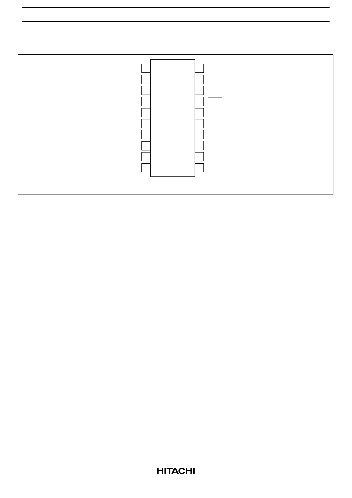
Pin Arrangement
P-RUN
GND
NC
NC 1
2
3
4
5
6
7
8
9
10
11
12
13
14
15
16
17
18
19
20 NC
(Top view)
Rf
Cf
R
C
R
R
V
Oadj
V
OUT
STBY
V
RES
NMI
C
V
V
NC
STBYadj
V
NMIadj
RES
CONT
CC
Page 3

HA16103 FPJ/FPK
3
Pin Functions
No. Pin Name Description
1 NC NC pin
2 P-RUN P-RUN signal input pin for watchdog timer
3 Rf Connect resistor Rf. Frequency bandwidth of the filter circuit depends on Rf
4 Cf Connect resistor Cf. Frequency bandwidth of the filter circuit depends on Cf
5R
R
Connect resistor RR. Reset-signal power-on time depends on R
R
6C
R
Connect resistor CR. Reset-signal power-on time depends on C
R
7 GND Ground
8 Voadj 5-V reference voltage fine-tuning pin. Connect a resistor between this pin and
GND. The value of output voltage is given by
V
OUT
= {1 + 5.34/(R1 // 2.0)} × Voadj Unit for R1: kΩ
9V
OUT
Connect the collector of an external PNP-type transistor. The pin supplies 5-V
regulated voltage for internal circuit
10 NC NC pin
11 NC NC pin
12 V
CONT
The external PNP-type transistor’s base control pin
13 V
CC
Supply voltage pin. Operating supply voltage range is 6.0 to 40 V.
14 C
RES
If the voltage of V
OUT
pin declines to less than Detection voltage(1) (because of
an instant power cut or other cause), NMI signals are generated.
If t
RES
≈ 0.5•Rf•C
RES
(sec) has passed since then, RES signals are generated.
If the voltage of V
OUT
pin inclines to more than Detection voltage(1) (in case of
re-start from LVI state), NMI signals are stop. t
r
≈ 0.5•Rf•C
RES
(sec) has passed
since then, RES signals are stop. Connect capacitor C
RES
between this pin and
GND to adjust the RES signals delay time(t
RES
, tr). If delay time is unnecessary,
make this pin open (t
RES
= 2 µs typ. tr = 10 µs typ. at open)
15 V
NMIadj
NMI detection voltage fine-tuning pin. Connect a resistor between this pin and
V
OUT
pin or GND. The value of output voltage is given by
V
NMI
= {1 + (R2 // 25.5)/(R3 // 10.6)} × V
NMIadj
. Unit for R2, R3: kΩ
16 NMI NMI signal output pin. Connect to pin NMI of the microcomputer
17 RES RES signal output pin. Connect to pin RES of the microcomputer
18 V
STBYadj
STBY detection voltage tuning pin. Connect a resistor between this pin and
V
OUT
or GND. The value of output voltage is given by
V
STBY
= 1.89 × {1 + 21/(7.9 + 8.85 // R4)} × V
STBYadj
Unit for R4: kΩ
19 STBY STBY signal output pin. Connect to pin STBY of the microcomputer
20 NC NC pin
Page 4
HA16103 FPJ/FPK
4
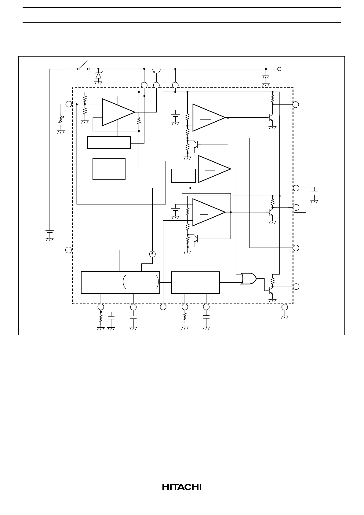
Block Diagram
Error
amplifier
Comparator
for STBY
Starter circuit
Reference
voltage
generator
Delay
circuit
Comparator
for RES
Comparator
for NMI
Power on reset
and automatic
reset circuit
Band-pass
filter circuit
Watchdog
timer
3
R
f
4
C
15 5 6
7
GND
17
C
RES
RES
V
STBYadj
18
16
NMI
14
19
STBY
V
CC
912
V
CONT
13
8
P-RUN
2
5.34 k
2 k
3.3 k
Ω
Ω
V
OUT
V
oadj
Ω
R
R
C
R
V
NMIadj
f
V
OUT
3.3 k
Ω
3.3 k
Ω
+
1000 pF
Page 5
HA16103 FPJ/FPK
5
Functional Description
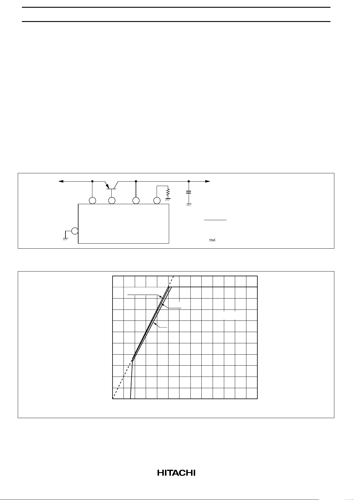
Stabilized Power Supply Function
The stabilized power supply includes the following features:
• Wide range of operating input voltage from 6 V to 40 V to provide stabilized voltages
• Availability of any output current, by simply replacing the external transistor
• Fine adjustment of output voltage
Figure 1 shows the fine adjustment circuit of the output circuit. Select the resistor R1 as shown in
equation 1.
Add a resistor between GND and Voadj to increase the output voltage.
HA16103
To microcomputer system
C1
100 µF
V
CC
V
GND
V
Q1
BATT
CONT
V
OUT
R
1
Vout = (1+ ) Voadj ⋅ ⋅ ⋅ ⋅ Equation 1
5.34
R // 2.0
×
1
(Voadj 1.31V)
(R1: kΩ)
Figure 1 Fine Adjustment Circuit of Output Voltage
0510
5
4
3
2
1
1 A
(Ta = 25°C)
Input voltage V
CC
(V)
Output voltage (V)
I = 0.1 A
OUT
0.5 A
1 : 1
Figure 2 Output Voltage Characteristic
Page 6
HA16103 FPJ/FPK
6
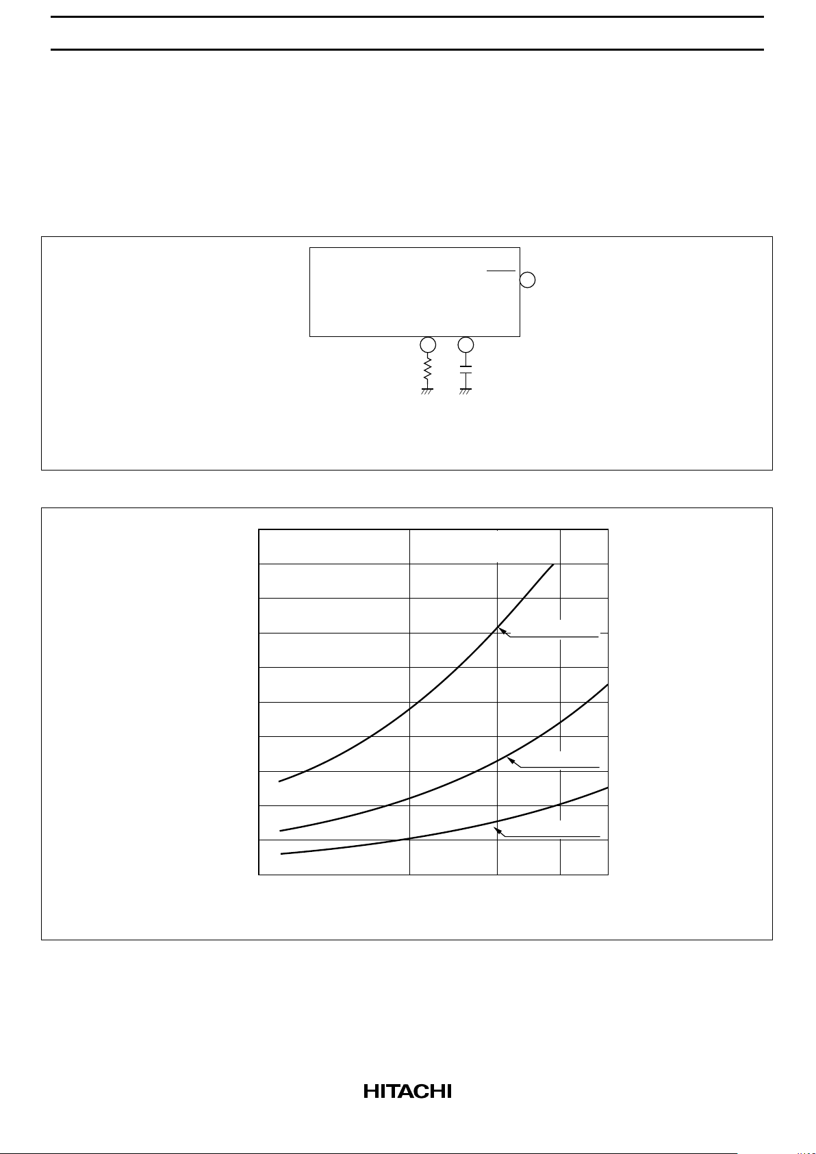
Power-On Reset Function
The system contains the power-on reset function required when a microcomputer is turned on.
The reset period may be set with external components RR and CR. Equation 2 specifies how to determine
the reset period (ton) and figure 3 shows the characteristic of the circuit.
RES
HA16103
RC
t = 0.46 x C x R x Vout(s) ⋅ ⋅ ⋅ ⋅ Equation 2
R : Ω
R
R
on
RR
R
200 m
180 m
160 m
140 m
120 m
100 m
80 m
60 m
40 m
20 m
0
Resistance R
R
(Ω)
(Ta = 25°C)
VCC = 12 V
CR = 0.22 µF
CR = 0.1 µF
CR = 0.047 µF
100 k 500 k200 k
Power-on time ton (s)
Figure 3 Characteristic of Power-On Reset Circuit
Page 7
HA16103 FPJ/FPK
7
Watchdog Timer Function
The system contains a bandpass filter for pulse width detection, which outputs a reset pulse when input
pulses are not at the preselected frequency (at either a higher or lower frequency).
The RC characteristic of the bandpass filter may be set with external components Rf and Cf. Equation 3
specifies how to determine the minimum pulse width (tmin) for runaway detection of the bandpass filter,
and figure 4 shows the characteristic of the filter.
HA16103
Rf Cf
tmin = Cf x Rf x 0.11 (s) ⋅ ⋅ ⋅ ⋅ Equation 3
Rf : Ω
2.0 m
1.8 m
1.6 m
1.4 m
1.2 m
1.0 m
0.8 m
0.6 m
0.4 m
0.2 m
Resistance Rf (Ω)
Cf = 0.022 µF
Cf = 0.01 µF
Cf = 0.0047 µF
100 k 500 k
Runaway-detection minimum pulse width tmin (s)
200 k
(Ta = 25°C)
P—Run pulse duty ratio 50% (fixed)
V = 12 V
C = 0.1 F
R = 180 k
CC
R
R
Ω
µ
Figure 4 Characteristic of Power-On Reset Circuit
Page 8

HA16103 FPJ/FPK
8
Low Voltage Monitoring Function
The system contains a circuit to send a control signal to the microcomputer when the output voltage drops.
The circuit includes the following features.
• Two-point monitoring of output voltage (V
NMI
and V
STBY
)
• Availability of fine adjustment of Vth1 (V
NMI
) and Vth2 (V
STBY
)
• Output of control signal in standby mode of microcomputer
Figure 5 shows the timing chart of control signals when the output voltage drops.
If the output voltage drops below Vth1 (4.60 V), the NMI signal rises to request the microcomputer to issue
the NMI interrupt signal. The RES signal falls t
RES
seconds after the NMI signal rises. If the output voltage
drops further to below Vth2 (3.2 V), the STBY signal rises to enable the micro-computer to enter standby
mode.
RES
STBY
P-RUN
NMI
V
O
V
BATT
4.70 V
4.60 V
4.70 V 4.60 V
3.20 V
toff
Power on reset signal
Automatic reset signal
System runaway
ton
t
RHtRL
t
RES
t
r
t
RES
Figure 5 Timing Chart for Low Voltage Monitoring
Page 9

HA16103 FPJ/FPK
9
Absolute Maximum Ratings (Ta = 25°C)
Ratings
Item Symbol HA16103FPJ HA16103FPK Units
VCC supply voltage V
CC
40 40 V
Control pin voltage V
CONT
40 40 V
Control pin current I
CONT
20 20 mA
V
OUT
pin voltage V
OUT
12 12 V
Power dissipation P
T
400*
1
400*
2
mW
Operating ambient temperature range Topr –40 to +85 –40 to +125 °C
Storage temperature range Tstg –50 to +125 –50 to +150 °C
Notes: 1. Value under Ta ≤ 77°C. If Ta is greater, 8.3 mW/°C derating occurs.
2. Allowable temperature of IC junction part, Tj
(max), is as shown below.
Tj (max) = θj-a•Pc (max)+Ta
(θj-a is thermal resistance value during mounting, and Pc (max) is the maximum value of IC
power dissipation.)
Therefore, to keep Tj (max) ≤ 125°C, wiring density and board material must be selected
according to the board thermal conductivity ratio shown below.
Be careful that the value of Pc (max) does not exceed that P
T
.
40 mm
Board
0.8 t ceramic or
1.5 t epoxy
0.5
12
5
10
20
Board thermal conductivity (W/m°C)
SOP20
using paste
containing
compound
SOP20
without compound
240
Thermal resistance (°C/W)
θj–a
220
200
180
160
140
120
100
80
Glass epoxy board with 10% wiring density
Glass epoxy board with 30% wiring density
Ceramic board with 96% alumina coefficient
(1)
(2)
(3)
(1) (2) (3)
Page 10

HA16103 FPJ/FPK
10
Electrical Characteristics (Ta = 25°C, VCC = 12 V, V
OUT
= 5 V)
HA16103FPJ/FPK
Item Symbol Min Typ Max Unit Test Condition
Supply current I
CCL
— 8 12 mA VCC = 12 V
Regulator Output voltage V
O1
4.80 5.00 5.20 V VCC = 6 to 17.5 V
I
OUT
= 0.5 A,
R
1
= 30 kΩ
V
O2
4.70 5.00 5.30 V VCC = 6 to 17.5 V
I
OUT
= 1 A, R1 = 30 kΩ
Line regulation Voline –50 — 50 mV VCC = 6 to 17.5 V
I
OUT
= 1 A, R1 = 30 kΩ
Load regulation Voload –100 — 100 mV I
OUT
= 10 mA to 0.5 A,
R
1
= 30 kΩ
Ripple rejection R
REJ
45 75 — dB Vi = 0.5 Vrms,
fi = 1 kHz, R
1
= 30 kΩ
Output voltage
Temperature
coefficient
δVO/δ
T
— 0.6 — mV/°CVCC = 12 V, R1 = 30 kΩ
Clock input “L”-input voltage V
IL
— — 0.8 V
“H”-input voltage V
IH
2.0 — — V
“L”-input current I
IL
–120 –60 — µAV
IL
= 0 V
“H”-input current I
IH
— 0.3 0.5 mA VIH = 5 V
Page 11

HA16103 FPJ/FPK
11
Electrical Characteristics (Ta = 25°C, VCC = 12 V, V
OUT
= 5 V) (cont)
Item Symbol Min Typ Max Unit Test Condition
NMI output NMI pin
“L”-level voltage
V
OL1
— — 0.4 V I
OL1
= 2 mA
NMI pin
“H”-level voltage
V
OH1
—V
O1
(VO2)
—V
NMI function start
V
OUT
voltage
V
NMI
— 0.7 1.4 V
STBY
output
STBY pin
“L”-level voltage
V
OL2
— — 0.4 V I
OL2
= 2 mA
STBY pin
“H”-level voltage
V
OH2
—V
O1
(VO2)
—V
STBY function start
V
OUT
voltage
V
STBY
— 0.7 1.4 V
RES output RES pin
“L”-level voltage
V
OL3
— — 0.4 V I
OL3
= 2 mA
RES pin
“H”-level voltage
V
OH3
—V
O1
(VO2)
—V
RES function start
V
OUT
voltage
V
RES
— 0.7 1.4 V
Power on time t
ON
25 40 60 ms Rf = 180 kΩ, RR = 180 kΩ
Clock off reset time t
OFF
80 130 190 ms
Cf = 0.01 µF, C
R
= 0.1 µF
Reset pulse
“L”-level time
t
RL
15 20 30 ms Rf = 180 kΩ, RR = 180 kΩ
Cf = 0.01 µF, C
R
= 0.1 µF
Reset pulse
“H”-level time
t
RH
37 60 90 ms Rf = 180 kΩ, RR = 180 kΩ
Cf = 0.01 µF, C
R
= 0.1 µF
Low Voltage Detection voltage(1) V
H1
4.40 4.60 4.80 V
protecton
Detection voltage(1)
Hysteresis width
V
HYS1
50 100 150 mV
Detection voltage(2) V
H2
2.9 3.2 3.5 V
Detection voltage(2)
Hysteresis width
V
HYS2
1.35 1.5 1.65 V
Reset
pulse
inhibit t
RES
— 200 — µsC
RES
= 2200 pF
Delay time
restart t
r
— 200 — µsC
RES
= 2200 pF
Page 12

HA16103 FPJ/FPK
12
Electrical Characteristics (Ta = –40 to 125°C, VCC = 12 V, V
OUT
= 5 V, R1 = 30 k)
(cont)
HA16103FPK
Item Symbol Min Typ Max Unit Test Condition
Supply current I
CC1
— 7 13 mA
Regulator Output voltage V
out1
4.80 5.00 5.20 V VCC = 6 to 17.5 V
I
OUT
= 0.5 A
Line regulation Voline –50 — 50 mV VCC = 6 to 17.5 V
I
OUT
= 0.5 A
Load regulation Voload –100 — 100 mV I
OUT
= 10 mA to 0.5 A
Clock input “L”-input voltage V
IL
— — 0.4 V
“H”-input voltage V
IH
2.4 — — V
“L”-input current I
IL
–120 –60 — µAV
IL
= 0 V
“H”-input current I
IH
— 0.3 0.6 mA VIH = 5 V
NMI output NMI pin
“L”-level voltage
V
OLN
— — 0.5 V I
OL1
= 2 mA
NMI pin
“H”-level voltage
V
OHN
—V
OUT1
—V
STBY
output
STBY pin
“L”-level voltage
V
OLS
— — 0.5 V I
OL2
= 2 mA
STBY pin
“H”-level voltage
V
OHS
—V
OUT1
—V
RES output RES pin
“L”-level voltage
V
OLR
— — 0.5 V I
OL3
= 2 mA
RES pin
“H”-level voltage
V
OHR
—V
OUT1
—V
Power on time t
ON
25 40 60 ms Rf = 180 kΩ, RR = 180 kΩ
Clock off reset time t
OFF
70 130 200 ms Cf = 0.01 µF, CR = 0.1 µF
Reset pulse
“L”-level time
t
RL
15 20 30 ms Rf = 180 kΩ, RR = 180 kΩ
Cf = 0.01 µF, C
R
= 0.1 µF
Reset pulse
“H”-level time
t
RH
30 60 100 ms Rf = 180 kΩ, RR = 180 kΩ
Cf = 0.01 µF, C
R
= 0.1 µF
Low Voltage Detection voltage(1) V
NMI
4.35 4.60 4.85 V
protecton
Detection voltage(2) V
STBY
2.80 3.20 3.60 V
Page 13

HA16103 FPJ/FPK
13
Test Circuit
V
BATT
C
RES
2200 p
180 k
180 k
0.01
µ
0.1
µ
V
STBYadj
C
R
R
R
V
NMIadj
NMI
STBY
RES
V
CCVCONT
V
OUT
Voadj
S
1
GND
100 µ
Q1
Cf
RfP-RUN
C
1
Counter
HA16103
2SB857D
V
OUT
R
1
1000 p
Unit R:
C: F
Ω
Sample Connection Circuit
Sample Connection Circuit between HA16103 and H8/532
(1)
VCCV
CONT
V
OUT
V
oadj
V
NMIadj
NMI
STBY
RES
V
STBYadj
C
RES
C
R
R
R
C
f
R
f
P-RUN
GND
V
Z2
C
2
R
5
V
BATT
C
RES
2200 p
180 k
180 k
0.01
µ
0.1
µ
R
4
R
3
R
2
R
1
C
1
100 µ
V
Z1
IGN,SW
S
1
Q1
Q2
Q3
V
CC
NMI
STBY
RES
GND
HA16103
H8/532
To other
microcomputer systems
PORT
D
1
1000 p
Unit R:
C: F
Ω
Page 14

HA16103 FPJ/FPK
14
Sample Connection Circuit between HA16103 and H8/532 (2)
S1
IGN. SW
R5
C2
V
Z2
V
Z1
Q1
R1
R2
C1
100 µ
Q2
Q3
R4
2200 p0.1 µ180 k0.01 µ
180 k
1000 p
GND
CLK
Rf Cf R C
V
RES
STBY
NMI
VNMIadj
V
CC
VVVoadj
HA16103
V
PORT
GND
H8/532
RES
STBY
NMI
V
CC
CLK
HA16103
GND
RES
STBY
NMI
PORT
GND
H8/532
RES
STBY
V
CC
NMI
2200 p
0.1 µ
180 k0.01 µ
180 k
1000 p
BATT
CONT
OUT
STBYadj
RR
V
OUT
Rf Cf R C
RR
R3
C
RES
V
STBYadj
C
RES
Unit R:
C: F
Ω
Page 15

HA16103 FPJ/FPK
15
Precautions
If the IC’s ground potential varies suddenly by several volts due to wiring impedance (see figure 6), a false
RES pulse may be output. The reason for this is that potentials in the RES pulse generating circuit change
together with the V
OUT
-GND potential. The reference potential of the comparator in figure 7 and the
potential of the external capacitor have different impedances as seen from the comparator, causing a
momentary inversion. The solution is to stabilize the ground potential. Two ways of stabilizing the IC’s
ground line are:
• Separate the IC’s ground line from highcurrent ground lines.
• Increase the capacitance (Co) used to smooth the V
OUT
output.
Wiring impedance
HA16103PJ/FPJ
Co
R
L
SW2
SW1
V
IGN
Wiring impedance
Relay or other load
Figure 6 Typical Circuit
GND
RES
Vout
VcontV
CC
+
–
C
RES
Wiring impedance
GND
RES
Vout
Vcont
CC
+
–
C
RES
Wiring impedance
Figure 7 RES Comparator
Page 16

HA16103 FPJ/FPK
16
Permissible P-RUN
duty cycle
AB
duty =
B
A + B
100×
Runaway detected
at 100%
Ta = 25°C
V = 12 V
IN
T = 25°C
V = 12 V
R = 30 k
a
CC
1
Ω
Rf = 360 kΩ
Rf = 560 kΩ
Rf = 180 kΩ
3 m
2 m
1 m
1000 p 2000 p 3000 p 5000 p 7000 p 10000 p0
Low-Voltage Reset Pulse Delay t
RES
(sec)
C (F)
RES
20 k
10 k
5 k
20 40 60 80 1000
P-RUN Pulse Frequency (Hz)
P-RUN Pulse Duty Cycle (%)
2 k
1 k
500
200
100
50
20
10
• Low-voltage inhibit section
Low-Voltage Reset Pulse Delay vs. C
RES
Permissible P-RUN Pulse Duty Cycle vs. P-RUN Pulse Frequency
Page 17

HA16103 FPJ/FPK
17
Ta = 25°C
V = 12 V
R = 30 k
CC
1
Ω
Rf = 360 kΩ
3 m
2 m
1 m
1000 p 2000 p 3000 p 5000 p 7000 p 10000 p0
Low-Voltage Reset Pulse Recovery Delay t
r
(sec)
C (F)
RES
Rf = 560 kΩ
Rf = 180 kΩ
100 k 200 k 300 k 500 k
0
Reset Low Time t
RL
(s)
Resistance RR (Ω)
160 m
140 m
120 m
100 m
80 m
60 m
40 m
20 m
• Power-on and auto-reset section
Reset Low Time vs. Resistance R
R
C = 0.22 µF
R
C = 0.047 µF
R
C = 0.1 µF
R
Ta = 25°C
V = 12 V
V = 5 V typ
CC
OUT
• Low-voltage inhibit section
Low-Voltage Reset Pulse Recovery Delay vs. C
RES
Page 18

HA16103 FPJ/FPK
18
100 k 200 k 300 k 500 k
0
Clock-Off Time t
OFF
(s)
C = 0.22 µF
R
700 m
600 m
500 m
400 m
300 m
200 m
100 m
C = 0.1 µF
Resistance R
R
(Ω)
C = 0.047 µF
R
Ta = 25°C
V = 12 V
V = 5 V typ
CC
OUT
R
10 k 100 k 1 M0
Output Voltage V
OUT
(V)
V
OUT
Adjustment Resistance R1 (Ω)
5.30
5.20
5.10
5.00
4.90
4.80
4.70
Ta = 25°C
V = 12 V
CC
• Vref section
Output Voltage vs. Adjustment Resistance
• Power-on and auto-reset section
Clock-Off Time vs. Resistance R
R
Page 19

HA16103 FPJ/FPK
19
C = 0.047 µF
R
100 k 200 k 300 k 500 k
0
C = 0.22 µF
R
280 m
260 m
240 m
220 m
200 m
180 m
160 m
140 m
120 m
100 m
80 m
60 m
40 m
20 m
C = 0.1 µF
R
Ta = 25°C
V = 12 V
V = 5 V typ
CC
OUT
Reset High Time t
RH
(s)
Resistance RR (Ω)
• Power-on and auto-reset section
Reset High Time vs. Resistance R
R
Page 20

HA16103 FPJ/FPK
20
Package Dimensions
Hitachi Code
JEDEC
EIAJ
Mass
(reference value)
FP-20DA
—
Conforms
0.31 g
Unit: mm
*Dimension including the plating thickness
Base material dimension
*0.42 ± 0.08
0.12
0.15
M
20
10
1
*0.22 ± 0.05
0.80 Max
11
12.6
5.5
2.20 Max
13 Max
0° – 8°
0.70 ± 0.20
+ 0.20
– 0.30
7.80
1.27
0.10 ± 0.10
1.15
0.40
± 0.06
0.20 ± 0.04
Page 21

HA16103 FPJ/FPK
21
Cautions
1. Hitachi neither warrants nor grants licenses of any rights of Hitachi’s or any third party’s patent,
copyright, trademark, or other intellectual property rights for information contained in this document.
Hitachi bears no responsibility for problems that may arise with third party’s rights, including
intellectual property rights, in connection with use of the information contained in this document.
2. Products and product specifications may be subject to change without notice. Confirm that you have
received the latest product standards or specifications before final design, purchase or use.
3. Hitachi makes every attempt to ensure that its products are of high quality and reliability. However,
contact Hitachi’s sales office before using the product in an application that demands especially high
quality and reliability or where its failure or malfunction may directly threaten human life or cause risk
of bodily injury, such as aerospace, aeronautics, nuclear power, combustion control, transportation,
traffic, safety equipment or medical equipment for life support.
4. Design your application so that the product is used within the ranges guaranteed by Hitachi particularly
for maximum rating, operating supply voltage range, heat radiation characteristics, installation
conditions and other characteristics. Hitachi bears no responsibility for failure or damage when used
beyond the guaranteed ranges. Even within the guaranteed ranges, consider normally foreseeable
failure rates or failure modes in semiconductor devices and employ systemic measures such as failsafes, so that the equipment incorporating Hitachi product does not cause bodily injury, fire or other
consequential damage due to operation of the Hitachi product.
5. This product is not designed to be radiation resistant.
6. No one is permitted to reproduce or duplicate, in any form, the whole or part of this document without
written approval from Hitachi.
7. Contact Hitachi’s sales office for any questions regarding this document or Hitachi semiconductor
products.
Hitachi, Ltd.
Semiconductor & Integrated Circuits.
Nippon Bldg., 2-6-2, Ohte-machi, Chiyoda-ku, Tokyo 100-0004, Japan
Tel: Tokyo (03) 3270-2111 Fax: (03) 3270-5109
Copyright ' Hitachi, Ltd., 1998. All rights reserved. Printed in Japan.
Hitachi Asia Pte. Ltd.
16 Collyer Quay #20-00
Hitachi Tower
Singapore 049318
Tel: 535-2100
Fax: 535-1533
URL NorthAmerica : http:semiconductor.hitachi.com/
Europe : http://www.hitachi-eu.com/hel/ecg
Asia (Singapore) : http://www.has.hitachi.com.sg/grp3/sicd/index.htm
Asia (Taiwan) : http://www.hitachi.com.tw/E/Product/SICD_Frame.htm
Asia (HongKong) : http://www.hitachi.com.hk/eng/bo/grp3/index.htm
Japan : http://www.hitachi.co.jp/Sicd/indx.htm
Hitachi Asia Ltd.
Taipei Branch Office
3F, Hung Kuo Building. No.167,
Tun-Hwa North Road, Taipei (105)
Tel: <886> (2) 2718-3666
Fax: <886> (2) 2718-8180
Hitachi Asia (Hong Kong) Ltd.
Group III (Electronic Components)
7/F., North Tower, World Finance Centre,
Harbour City, Canton Road, Tsim Sha Tsui,
Kowloon, Hong Kong
Tel: <852> (2) 735 9218
Fax: <852> (2) 730 0281
Telex: 40815 HITEC HX
Hitachi Europe Ltd.
Electronic Components Group.
Whitebrook Park
Lower Cookham Road
Maidenhead
Berkshire SL6 8YA, United Kingdom
Tel: <44> (1628) 585000
Fax: <44> (1628) 778322
Hitachi Europe GmbH
Electronic components Group
Dornacher Straβe 3
D-85622 Feldkirchen, Munich
Germany
Tel: <49> (89) 9 9180-0
Fax: <49> (89) 9 29 30 00
Hitachi Semiconductor
(America) Inc.
179 East Tasman Drive,
San Jose,CA 95134
Tel: <1> (408) 433-1990
Fax: <1>(408) 433-0223
For further information write to:
 Loading...