

Page 1
HI-SINCERITY
MICROELECTRONICS CORP.
Spec. No. : HP200201
Issued Date : 2000.10.01
Revised Date : 2002.07.12
Page No. : 1/8
HS200207
H1563P / H1563S
HIGH-EFFICIENCY DC/DC CONVERTER
Description
The H1563 is a monolithic control circuit containing the primary functions required for DC to DC converters
and highside-sensed constant current source. The device consists of an internal temperature compensated reference, comparator, controlled duty cycle oscillator with an active current sense circuit, bootstrapped driver, and high current output switch. This device is specifically designed to construct a constant
current source for battery chargers with a minimum number of external components. Bootstrapped driver
can drive the NPN output switch to saturation for higher eff-iciency and less heat dissipation. The H1563
can deliver 1.5A continuous current without requiring a heat sink.
Features
• 3V to 40V Input Voltage Operation
• Internal 2A Peak Current Switch
• 1.5A Continuous Output Current
• Bootstrapped Driver
• High Side Current Sense Capability
• High Efficiency (up to 90%)
• Internal ±2% Reference
• Low Quiescent Current at 1.6mA
• Frequency Operation from 100Hz to 100KHz
Applications
• Constant Current Source for Battery Chargers
• Saver for Cellular Phone
• Step-Down DC-DC Converter Module
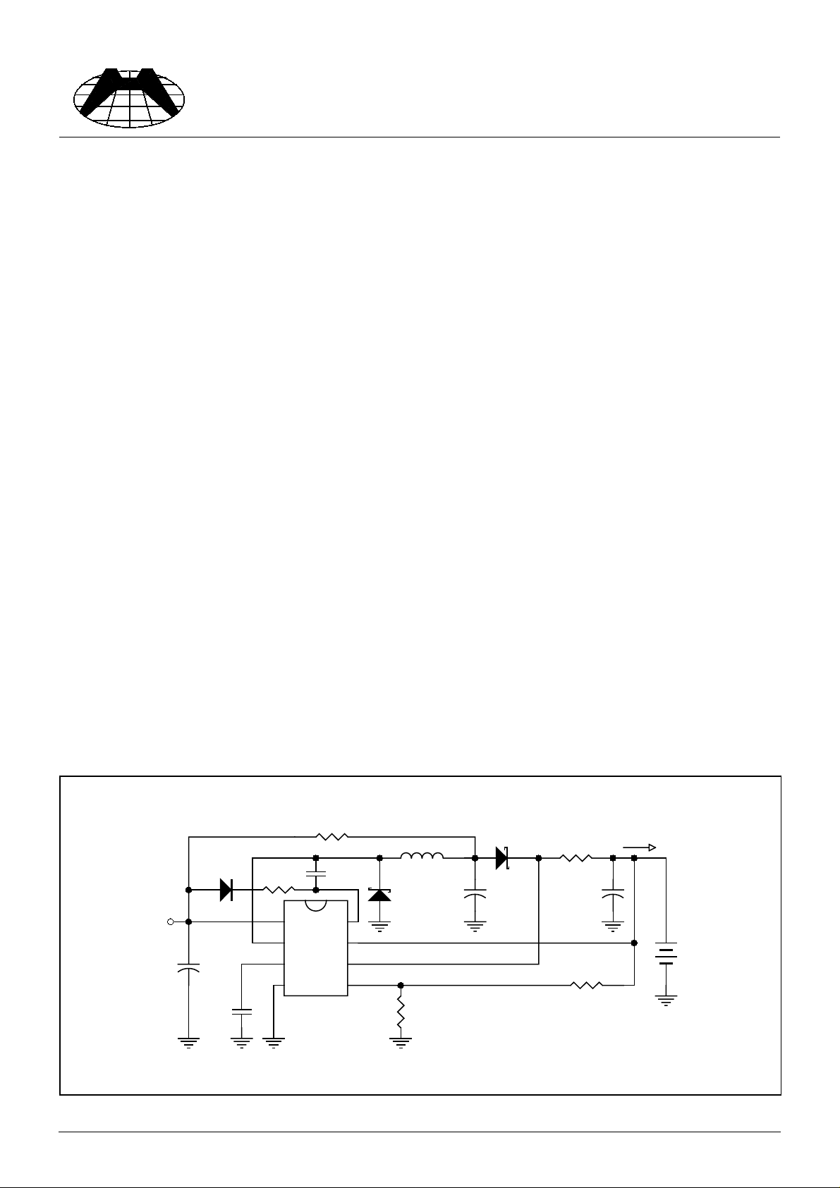
T y pical Application Circuit
Saver Circuit for Cellular Phone
R1
1K
Vin
+
D2
H1N4148
C1
220uF
CT
470pF
R2
120
C3
1uF
SC BST
SE IS
TC VCC
GND FB
H1563
L
220uH
D1
H1N5821
RA
5.6K
D3
H1N5819
+ +
Co
220uF
*RS
C5
10uF
RB
33K
Io
*Io=300mV/RS
H1563P / H1563S HSMC Product Specification
Page 2
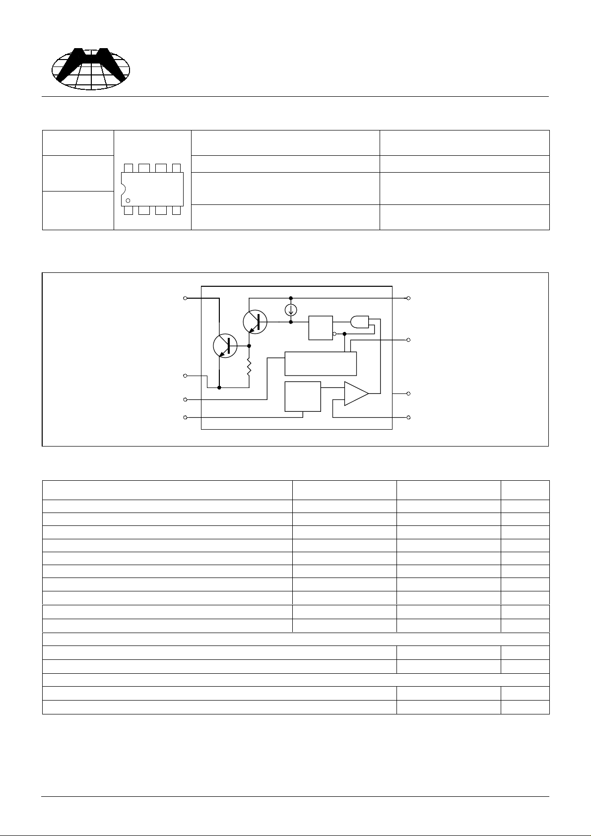
Pin Connections
HI-SINCERITY
MICROELECTRONICS CORP.
Spec. No. : HP200201
HS200207
Issued Date : 2000.10.01
Revised Date : 2002.07.12
Page No. : 2/8
Order No. Pin1: SC-2A Switch Collector
H1563P
Top View
Pin2: SE-Darlington Switch Emitter Pin6: VCC-Power Supply Input
5678
(Plastic DIP)
Pin3: TC-Oscillator Timing Capacitor
H1563S
(Plastic SO)
4321
Pin4: GND-Power Ground
Block Diagram
1
SC
Q2
CT Is
Oscillator
1.25V
Reference
Voltage
SE
TC
Q1
2
3
4
80
Pin5: FB-Feedback Comparator
Inverting Input
Pin7: IS-Highside Current Sense
Input
Pin8: BST-Bootstrapped Driver
Collector
8
BST
S
Q
R
+
Comparator
7
IS
6
VCC
5
FBGND
Absolute Maxium Rating
Rating Symbol Value Unit
Power Supply Voltage Vcc 40 Vdc
Comparator Input Voltage Range Vir 0.3 ~ +40 Vdc
Switch Collector Voltage Vc(switch) 40 Vdc
Switch Emitter Voltage (Vpin1=40V) Ve(switch) 40 Vdc
Switch Collector to Emitter Voltage Vce(switch) 40 Vdc
Driver Collector Voltage Vc(driver) 40 Vdc
Switch Current Isw 2 A
Operating Junction Temperature Tj 150
Operating Ambient Temperature Range Ta 0 to +70
Storage Temperature Range Tstg -65 to +150
DIP Package Power Dissipation and Thermal Characteristics:
Ta=25°C
Thermal Resistance 85
SO Package Power Dissipation and Thermal Characteristics:
Ta=25°C
Thermal Resistance 105
1.5 W
°C/W
1.2 W
°C/W
°C
°C
°C
H1563P / H1563S HSMC Product Specification
Page 3
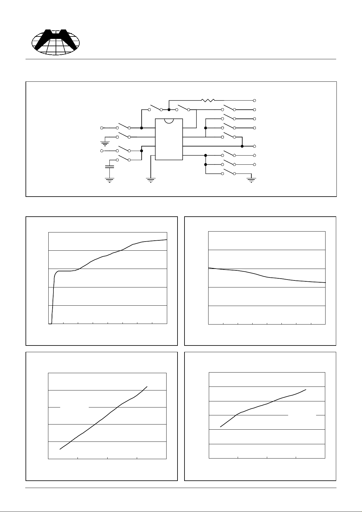
Test Circuit
HI-SINCERITY
MICROELECTRONICS CORP.
Spec. No. : HP200201
HS200207
Issued Date : 2000.10.01
Revised Date : 2002.07.12
Page No. : 3/8
Current Source
I
1A
2V/0V
DISCHG/ICHG
CT
1nF
Characteristics Curve
Standby Supply Current vs Supply Voltage
2
1.6
1.2
1
SC BST
2
SE IS
3
TC VCC
4
GND FB
H1563
R1
1K
8
7
6
5
VCC
20mA
Current Source
4.55V
@VCC=5V
4.75V
VCC
1.275V
1.225V
Vfb Theshol d Vol t age vs Temper ature
1.3
1.28
1.26
0.8
Icc Supply Cur rent (m A)
0.4
0
0 5 10 15 20 25 30 35 40
Vcc Suppl y Voltage (V)
Common Emitter Configuration Output Switch
Saturation Voltage vs Collector Current
1
0.8
0.6
0.4
Vce(sat) Saturation Voltage (V)
0.2
VCC=5V
PIN7=VCC
PIN 2,3,5=GND
Forced Beta=20
0
00.511.52
Ic Coll e c tor Current ( A )
1.24
Vfb Thresh ol d Voltage (V)
1.22
1.2
0 1020304050607080
Temperatu re (J)
VCC=5V
Ct=1nF
PIN2=GND
Emmiter Follower Configuration Output Switch
Saturtion Voltage vs Emmiter Current
1.8
1.7
1.6
1.5
1.4
Vce(sat) Sar urtion Vol tage ( V)
1.3
1.2
00.511.52
Ie Emitter (A)
VCC=5V
PIN1,7 ,8=VCC
PIN3,5=GND
H1563P / H1563S HSMC Product Specification
Page 4

HI-SINCERITY
MICROELECTRONICS CORP.
Spec. No. : HP200201
Issued Date : 2000.10.01
Revised Date : 2002.07.12
Page No. : 4/8
HS200207
Electrical Characteristics (Vcc=5V, Ta=25°C, unless otherwise specified)
Parameter Test Condition Symbol Min. Typ. Max. Unit
Oscillator
Charging Current
Discharge Current
5V≤V
5V≤V
CC≤40V
CC≤40V
Voltage Swing Pin3 VOSC -0.6- V
Discharge to Charge Current Ratio VIS =VCC IDischg/Ichg -6-
Current Limit Sense Voltage IChg=Idischg VCC-VIS 250 300 350 mV
Output Switch
Saturation Voltage, Emitter
Follower Connection
Saturation Voltage
SE=1A, VBST=VSC=VCC VCE(Sat) -11.3V
I
I
SC=1A, IBST=50mA
(Forced β ≈ 20)
DC Current Gain ISC=1A, VCE=5V hFE 35 120 -
Collector Off-State Current VCE=30V ICC(Off) -10-nA
Comparator
Threshold Voltage
Threshold Voltage Line Regulation
Ta=25°C
0°C≤Ta≤70°C
CC≤40V
3V≤V
Input Bias Current VIN=0V IIB - 20 400 nA
V
IS=VCC, VPin5>VFB
Supply Current
5V≤VCC≤40V, CT=1nF
Pin2=Gnd
Remaining pins open
I
chg 24 35 42 uA
I
dischg 140 220 260 uA
CE(Sat) -0.40.7V
V
VFB
REG
Line -36mV
1.227 1.25 1.273 V
1.21 - 1.29 V
ICC -1.63mA
Application Information
Design Formula Table
Calculation Step-Down Step-Up
ton / toff Vout+VF / (Vin(min) -Vsat-Vout) Vout+VF-Vin(min) / (Vin(min)-Vsat)
(ton+toff) max 1 / Fmin 1 / Fmin
CT 4*10-5ton 4*10-5ton
IC(switch) 2*Iout(max) 2*Iout(max)*(ton+toff / toff)
RS 0.3 / IC(switch) 0.3 / IC(switch)
L(min)
CO IC(switch)*(ton+toff) / 8VRipple(P-P)
Vsat: Saturation voltage of the output switch.
V
F: Forward voltage of the ringback rectifier.
The following power supply characteristics must be chosen:
V
in: Nominal input voltage.
V
out: Desired output voltage. |Vout|=1.25*(1+RB/RA)
I
out: Desired output current
Fmin: Minimum desired switching frequency at selected values for V
V
Ripple(P-P): Desired peak to peak output ripple voltage in practice, the calculated value will need to be increased due
to the capacitor equivalent series resistance and board layout. The ripple voltage should be kept to a low
value since it will directly effect the line and load regulation.
((Vin(min)-Vsat-Vout) / IC(switch))*ton(max) ((Vin(min)-Vsat) / IC(switch))*ton(max)
Iout*ton / VRipple(P-P)
in and Iout.
H1563P / H1563S HSMC Product Specification
Page 5

HI-SINCERITY
D1
MICROELECTRONICS CORP.
Application Information (Continuos)
Spec. No. : HP200201
HS200207
Issued Date : 2000.10.01
Revised Date : 2002.07.12
Page No. : 5/8
Fig.1 Step-Down Converter
RS
0.22
C1
100uF
D2
H1N4148
D2
H1N4148
R1
470
RS
0.22
Vin
8V~25V
+
C1
100uF
Fig.2 Step-Down Converter With External 5V Bootstrap
5V
Vin
16V~25V
+
C3
+
1uF
8
7
6
C3
+
1uF
8
7
6
H1563
H1563
R3
2.2M
GNDFB
D3
SCBST
SEIS
TCVCC
GNDFB
1
SCBST
2
SEIS
3
TCVCC
45
1
2
3
45
1N1418
R2
390K
C2
1000pF
L1
300uH
D1
H1N5819
RA
1K
5V/1A
+
C4
470uF
RB
3K
Line Regulation: 40mV (Vin=10V~20V, @Io=1A)
Load Regulation: 20mV (Vin=15V, @Io=100mA~1A)
Short Circuit Current: 1.3A (Vin=15V, @RL=0.1Ω)
C2
470pF
L1
300uH
D1
H1N5819
+
RA
1.5K
C4
470uF
RB
13K
12V/1A
Fig.3 Step-Up Converter
L
Vin
200uH
R1
150
8
RS
0.22
+
C1
100uF
RA
2.2K
7
6
H1563
1
SCBST
2
SEIS
3
TCVCC
45
GNDFB
H1N5819
CT
680pF
RB
47K
+
Co
220uF
Line Regulation: 100mV (Vin=8V~16V, @Io=200mA)
=
H1563P / H1563S HSMC Product Specification
Vout
28V/200mA
=
~
Page 6

HI-SINCERITY
MICROELECTRONICS CORP.
Fig.4 Step-Up Converter With External NPN Switch
L
R1
1
SCBST
2
SEIS
3
TCVCC
45
GNDFB
Vin
8
RA
7
6
H1563
RS
+
C1
CT
D1
R2
Q1
RB
Spec. No. : HP200201
HS200207
Issued Date : 2000.10.01
Revised Date : 2002.07.12
Page No. : 6/8
Vout
+
Co
Fig.5 Inverting Converter
Vin
4.5V~6V
8
RS
0.25
+
C1
100uF
RB
8.2K
7
6
H1563
RA
953
1
SCBST
2
SEIS
3
TCVCC
45
GNDFB
CT
600pF
Co
470uF
L
100uH
D1
H1N5819
Vout
-12V/100mA
Line Regulation: 20mV (Vin=4.5V~6V, @Io=100mA)
Load Regulation: 100mV (Vin=5V, @Io=10mA~100mA)
H1563P / H1563S HSMC Product Specification
Page 7

HI-SINCERITY
g
MICROELECTRONICS CORP.
H1563P Dimension (DIP-8P)
5
87
6
Spec. No. : HP200201
HS200207
Issued Date : 2000.10.01
Revised Date : 2002.07.12
Page No. : 7/8
Marking:
A
1
432
HP
15 63
Date Code
B
J
DIP-8P Plastic Package
DIM
F
α1
C
E
G
H
D
I
M
Inches Millimeters Inches Millimeters
Min. Max. Min. Max.
K
L
DIM
Min. Max. Min. Max.
HSMC Packa
e Code: P
A 0.2480 0.2520 6.29 6.40 H 0.0150 0.0210 0.38 0.53
B 0.3630 0.3670 9.22 9.32 I 0.0898 0.1098 2.28 2.79
C - *0.0600 - *1.52 J 0.2950 0.3050 7.49 7.74
D - *0.0500 - *1.27 K - *0.1181 - *3.00
E - *0.0390 - *0.99 L 0.3370 0.7470 8.56 8.81
F 0.1280 0.1320 3.25 3.35 M 0.0090 0.0150 0.229 0.381
G 0.1250 0.1400 3.17 3.55
Notes: 1.Dimension and tolerance based on our Spec. dated Sep. 07,1997.
2.Controlling dimension: millimeters.
3.Maximum lead thickness includes lead finish thickness, and minimum lead thickness is the minimum thickness of base material.
4.If there is any question with packing specification or packing method, please contact your local HSMC sales office.
Material:
• Lead: 42 Alloy; solder plating
• Mold Compound: Epoxy resin family, flammability solid burning class: UL94V-0
α194° 97° 94° 97°
*: Typical
H1563P / H1563S HSMC Product Specification
Page 8

HI-SINCERITY
g
MICROELECTRONICS CORP.
H1563S Dimension (SOP-8P)
Spec. No. : HP200201
HS200207
Issued Date : 2000.10.01
Revised Date : 2002.07.12
Page No. : 8/8
Top View
B
A
C
Right side View
G
I
H
Marking:
HS
15 63
Date Code
SOP-8P Plastic Package
D
Front View
Part A
J
E
Part A
M
K
L
N
HSMC Packa
e Code: S
O
F
DIM
Inches Millimeters Inches Millimeters
Min. Max. Min. Max.
DIM
Min. Max. Min. Max.
A 0.1909 0.2007 4.85 5.10 I 0.0019 0.0078 0.05 0.20
B 0.1515 0.1555 3.85 3.95 J 0.0118 0.0275 0.30 0.70
C 0.2283 0.2441 5.80 6.20 K 0.0074 0.0098 0.19 0.25
D 0.0480 0.0519 1.22 1.32 L 0.0145 0.0204 0.37 0.52
E 0.0145 0.0185 0.37 0.47 M 0.0090 0.0110 0.23 0.28
F 0.1472 0.1527 3.74 3.88 N 0.0031 0.0051 0.08 0.13
G 0.0570 0.0649 1.45 1.65 O 0.0000 0.0059 0.00 0.15
H 0.1889 0.2007 4.80 5.10
Notes: 1.Dimension and tolerance based on our Spec. dated Mar. 01, 2001.
Material:
• Lead: 42 Alloy; solder plating
• Mold Compound: Epoxy resin family, flammability solid burning class: UL94V-0
2.Controlling dimension: millimeters.
3.Maximum lead thickness includes lead finish thickness, and minimum lead thickness is the minimum thickness of base material.
4.If there is any question with packing specification or packing method, please contact your local HSMC sales office.
*: Typical
Important Notice:
• All rights are reserved. Reproduction in whole or in part is prohibited without the prior written approval of HSMC.
• HSMC reserves the right to make changes to its products without notice.
• HSMC semiconductor products are not warranted to be suitable for use in Life-Support Applications, or systems.
• HSMC assumes no liability for any consequence of customer product design, infringement of patents, or appl ication assistance.
Head Office And Factory:
• Head Office (Hi-Sincerity Microelectronics Corp.): 10F.,No. 61, Sec. 2, Chung-Shan N. Rd. Taipei Taiwan R.O.C.
Tel: 886-2-25212056 Fax: 886-2-25632712, 25368454
• Factory 1: No. 38, Kuang Fu S. Rd., Fu-Kou Hsin-Chu Industrial Park Hsin-Chu Taiwan. R.O.C
Tel: 886-3-5983621~5 Fax: 886-3-5982931
H1563P / H1563S HSMC Product Specification
 Loading...