

Page 1
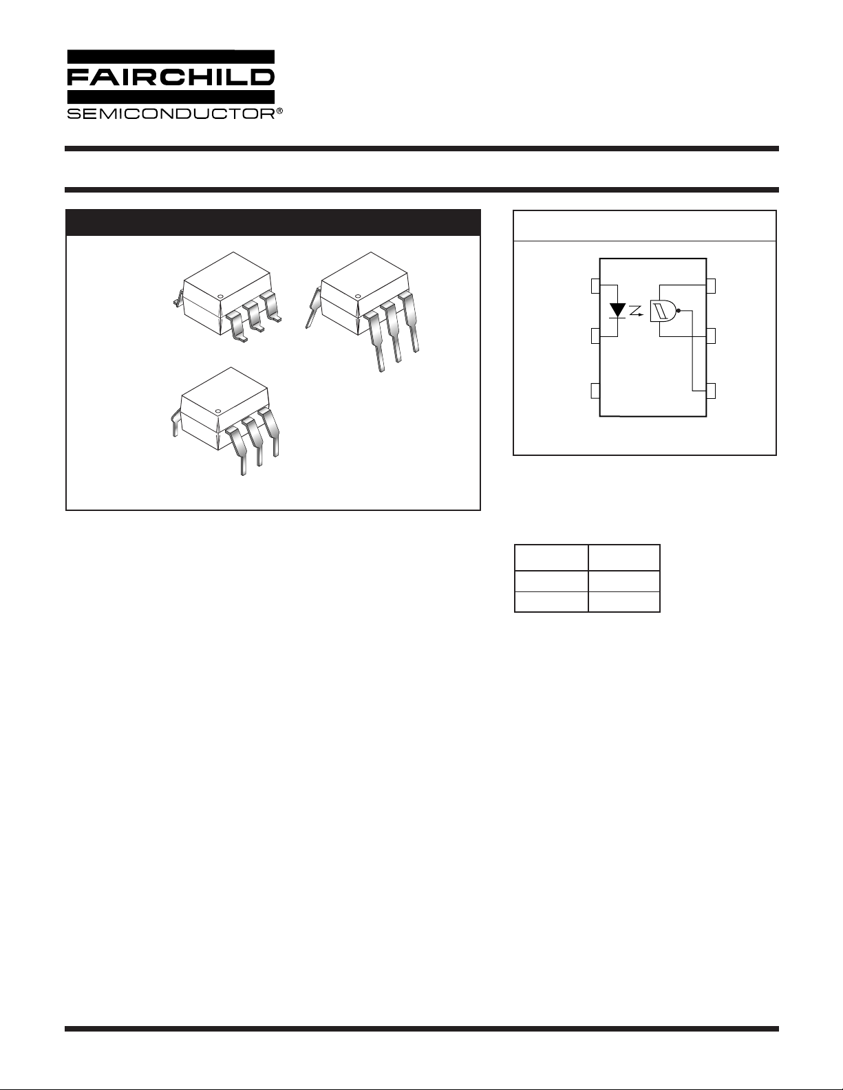
6-PIN DIP
HIGH SPEED LOGIC OPTOCOUPLERS
H11N1-M H11N2-M H11N3-M
PACKAGE
6
6
1
1
6
1
DESCRIPTION
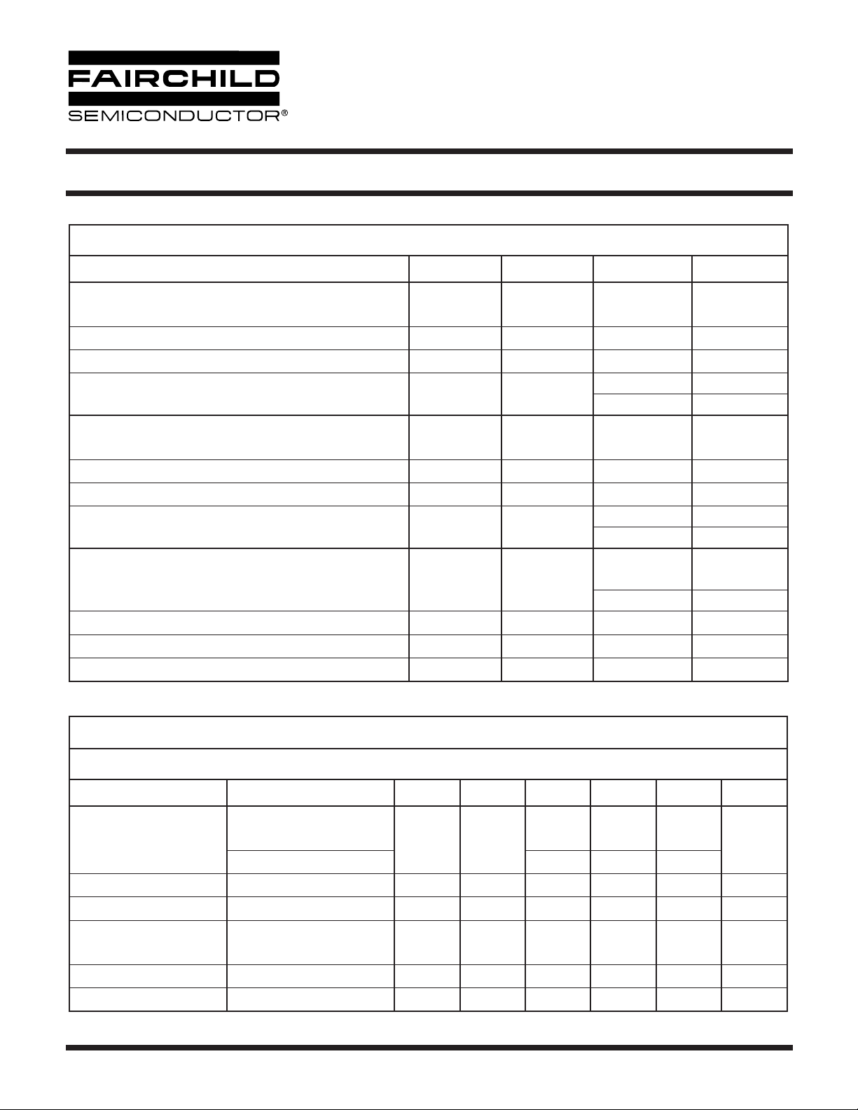
The H11NX-M series has a high speed integrated circuit detector optically
coupled to an AlGaAs infrared emitting diode. The output incorporates a
Schmitt trigger, which provides hysteresis for noise immunity and pulse s
haping. The detector circuit is optimized for simplicity of operation and utilizes
an open collector output for maximum application flexibility.
SCHEMATIC
1
ANODE
CATHODE
2
3
Truth Table
Input Output
HL
LH
V
6
CC
5GND
V
4
O
FEATURES
• High data rate, 5 MHz typical (NRZ)
•Free from latch up and oscilliation throughout voltage and temperature ranges.
• Microprocessor compatible drive
• Logic compatible output sinks 16 mA at 0.5 V maximum
• Guaranteed on/off threshold hysteresis
• Wide supply voltage capability, compatible with all popular logic systems
• High common mode transient immunity, 2000 V/µs minimum
•Fast switching t
• Underwriter Laboratory (UL) recognized—file #E90700
• VDE recognized – File#102497 – Add option V (e.g., H11N1VM)
= 7.5ns typical, t
r
= 12ns typical
f
APPLICATIONS
• Logic to logic isolator
• Programmable current level sensor
• Line receiver—eliminate noise and transient problems
• A.C. to TTL conversion—square wave shaping
• Interfaces computers with peripherals
• Isolated power MOS driver for power supplies
© 2003 Fairchild Semiconductor Corporation
Page 1 of 9
4/14/03
Page 2
6-PIN DIP
HIGH SPEED LOGIC OPTOCOUPLERS
H11N1-M H11N2-M H11N3-M
ABSOLUTE MAXIMUM RATINGS
Parameters Symbol Device Value Units
TOTAL DEVICE
Storage Temperature
Operating Temperature
Lead Solder Temperature
Total Device Power Dissipation @ 25°C
Derate Above 25°C 2.94 mW/°C
EMITTER
Continuous Forward Current
Reverse Voltage
Forward Current - Peak (1 µs pulse, 300 pps)
LED Power Dissipation 25°C Ambient
Derate Linearly From 25°C 1.41 mW/°C
DETECTOR
Detector Power Dissipation @ 25°C
Derate Linearly from 25°C 1.76 mW/°C
Allowed Range V
V
45
V
Allowed Range V
65
I
Output Current I
4
T
T
T
I
P
V
F
P
P
STG
OPR
SOL
D
I
F
R
(pk)
D
D
O
CC
O
All -55 to +150 °C
All -40 to +85 °C
All 260 for 10 sec °C
All
250 mW
All 30 mA
All 6 V
All 1.0 A
All
All
120 mW
150 mW
All 0 to 16 V
All 0 to 16 V
All 50 mA
ELECTRICAL CHARACTERISTICS
(T
= 0-70°C Unless otherwise specified.)
A
INDIVIDUAL COMPONENT CHARACTERISTICS
Parameters Test Conditions Symbol Device Min Typ* Max Units
EMITTER
= 10 mA
I
Input Forward Voltage
Reverse Current
F
I
= 0.3 mA
F
V
= 5 V I
R
Capacitance V = 0, f = 1.0 MHz
DETECTOR
Operating Voltage Range
I
Supply Current
Output Current, High
*Typical values at T
© 2003 Fairchild Semiconductor Corporation
= 25°C
A
= 0, V
F
I
= 0.3mA, V
F
= 5V I
CC
CC
= V
O
= 15V I
Page 2 of 9
V
F
R
C
J
V
CC
CC(off)
OH
All
0.75 1.25
All 10 µA
All 100 pF
All 4 15 V
All 6 10 mA
All 100 µA
1.4 2
4/14/03
V
Page 3

6-PIN DIP
HIGH SPEED LOGIC OPTOCOUPLERS
H11N1-M H11N2-M H11N3-M
TRANSFER CHARACTERISTICS
DC Characteristics Test Conditions Symbol Device Min Typ* Max Units
I
Supply Current
Output Voltage, low
Tu r n-On Threshold Current
Tu r n-Off Threshold Current
Hysteresis Ratio
= 10mA, V
F
R
=270 Ω ,V
L
R
=270 Ω , V
L
note 1
R
=270 Ω , V
L
R
=270 Ω , V
L
AC Characteristics Test Conditions Symbol Device Min Typ Max Units
= 5V I
CC
=5V, I
=I
CC
CC
CC
CC
F
= 5V
= 5V I
= 5V I
max. V
F(on)
CC(on)
I
F(off)
OL
F(on)
F(off)
/I
All 6.5 10 mA
All 0.5 V
H11N1-M 0.8 3.2
H11N3-M 4.1 10
All 0.3 mA
F(on)
All 0.65 0.95
mAH11N2-M 2.3 5
SWITCHING SPEED
Propagation delay time
High to Low
Rise Time
Propagation delay time
Low to High
Fall time
C=120pF, t
Fig. 1
C=120pF, t
Fig. 1
C=120pF, t
Fig. 1
C=120pF, t
Fig. 1
=1µs, R
P
=1µs, R
P
=1µs, R
P
=1µs, R
P
: Note 2
E
: Note 2
E
: Note 2
E
: Note 2
E
t
PHL
t
PLH
All 100 330 ns
t
r
All 7.5 ns
All 150 330 ns
t
f
All 12 ns
Data Rate All 5 MHz
ISOLATION CHARACTERISTICS
Parameters Test Conditions Symbol Min Typ* Max Units
Input-Output Isolation Voltage f = 60 Hz, t =1 sec.
V
Isolation Capacitance
Isolation Resistance
*Typical values at T
= 25°C
A
= 0V, f = 1 MHz C
I-O
V
= ±500 VDC R
I-O
V
ISO
ISO
ISO
7500
11
10
0.4 0.6 pF
NOTES:
1. Maximum I
is the maximum current required to trigger the output. For example, a 3.2mA maximum trigger current would
F(ON)
require the LED to be driven at a current greater than 3.2mA to guarantee the device will turn on. A 10% guard band is
recommended to account for degradation of the LED over its lifetime. The maximum allowable LED drive current is 30mA.
2. H11N1: R
H11N2: R
H11N3: R
= 910 Ω
E
= 560 Ω
E
= 240 Ω
E
V
PEAK
Ω
© 2003 Fairchild Semiconductor Corporation
Page 3 of 9
4/14/03
Page 4

6-PIN DIP
HIGH SPEED LOGIC OPTOCOUPLERS
H11N1-M H11N2-M H11N3-M
tr = tf ≤ 0.01µS
Z = 50Ω
C
I
F
H11N1-M
R
E
V
IN
1
2
I
6
6
5
Figure 1. Switching Test Circuit and Waveforms
Figure 2. Transfer Characteristics
6
V
5
4
3
2
- OUTPUT VOLTAGE (V)
Hysteresis area
O
V
shaded for illustration
1
0
01234
OH
I
F(OFF)
IF - INPUT CURRENT (mA)
I
F(ON)
VCC = 5V
= 270
R
L
= 25°C
T
A
V
OL
Ω
5V
VIN 5V
50%
0
R
270Ω
L
4
0.1µF
V
O
t
on
V
O
t
off
10%
90%
t
f
t
r
Figure 3. Threshold Current vs. Supply Voltage
1.4
1.2
1.0
0.8
0.6
0.4
0.2
- NORMALIZED THRESHOLD CURRENT
F
I
0.0
0246810121416
VCC - SUPPLY VOLTAGE (V)
TURN ON THRESHOLD
TURN OFF THRESHOLD
NORMALIZED TO:
TURN ON THRESHOLD AT
= 5V, TA = 25°C
V
CC
D
:
AT
Figure 4. Threshold Current vs. Temperature
1.2
1.0
I
0.8
F(Off)
, I
F(On)
0.6
0.4
CURRENT I
NORMALIZED THRESHOLD
0.2
0.0
010203040506070
F(On)
NORMALIZED TO :
V
CC
= 25°C
T
A
TA - TEMPERATURE (°C)
© 2003 Fairchild Semiconductor Corporation
= 5V
I
F(Off)
Page 4 of 9
Figure 5. Load Current vs. Output Voltage
100
IF = I
F(ON)
V
= 5V
10
- LOAD CURRENT (mA)
O
I
1
0.0 0.2 0.4 0.6 0.8 1.0
VO - OUTPUT VOLTAGE, LOW (V)
CC
4/14/03
Page 5

6-PIN DIP
HIGH SPEED LOGIC OPTOCOUPLERS
H11N1-M H11N2-M H11N3-M
Figure 6. Supply Current vs. Supply Voltage Figure 7. LED Forward Voltage vs. Forward Current
12
100
10
8
6
4
- SUPPLY CURRENT (mA)
C
I
2
0
24681012 14 16
TA = -25°C
TA = 25°C
TA = 85°C
ON STATE IF = 10mA
OFF STATE IF = 0
VCC - SUPPLY VOLTAGE (V)
TA = 85°C
10
- FORWARD CURRENT (mA)
F
I
1
1.0 1.2 1.4 1.6 1.8 2.0
VF - FORWARD VOLTAGE (V)
TA = -25°C
TA = 25°C
© 2003 Fairchild Semiconductor Corporation
Page 5 of 9
4/14/03
Page 6

6-PIN DIP
)
)
)
)
)
)
HIGH SPEED LOGIC OPTOCOUPLERS
H11N1-M H11N2-M H11N3-M
Package Dimensions (Through Hole) Package Dimensions (Surface Mount)
0.350 (8.89)
0.320 (8.13)
0.014 (0.36)
0.010 (0.25)
0.260 (6.60)
0.240 (6.10)
0.100 [2.54]
0.390 (9.90)
0.332 (8.43)
0.012 (0.30)
0.008 (0.20)
0.320 (8.13)
0.035 (0.88)
0.006 (0.16)
0.070 (1.77)
0.040 (1.02)
0.200 (5.08)
0.115 (2.93)
0.100 (2.54)
0.015 (0.38)
0.020 (0.50)
0.016 (0.41)
0.350 (8.89)
0.320 (8.13)
0.014 (0.36)
0.010 (0.25)
0.100 (2.54)
0.260 (6.60)
0.240 (6.10)
0.320 (8.13)
15°
0.012 (0.30)
0.070 (1.77)
0.040 (1.02)
0.200 (5.08)
0.115 (2.93)
0.025 (0.63)
0.020 (0.51)
0.020 (0.50)
0.016 (0.41)
Package Dimensions (0.4” Lead Spacing) Recommended Pad Layout for
0.350 (8.89)
0.320 (8.13)
Surface Mount Leadform
0.260 (6.60)
0.240 (6.10)
0.070 (1.77)
0.040 (1.02)
0.200 (5.08)
0.115 (2.93)
0.100 (2.54)
0.015 (0.38)
0.020 (0.50)
0.016 (0.41)
0.014 (0.36)
0.010 (0.25)
0.100 [2.54]
© 2003 Fairchild Semiconductor Corporation
0.012 (0.30)
0.008 (0.21)
0.425 (10.80)
0.400 (10.16)
Page 6 of 9
0.425 (10.79
0.100 (2.54
0.305 (7.75
0.070 (1.78
0.060 (1.52
0.030 (0.76
4/14/03
Page 7

6-PIN DIP
HIGH SPEED LOGIC OPTOCOUPLERS
H11N1-M H11N2-M H11N3-M
ORDERING INFORMATION
Option/Order Entry Identifier Description
S Surface Mount Lead Bend
SR2 Surface Mount; Tape and reel
T 0.4" Lead Spacing
V VDE 0884
TV VDE 0884, 0.4" Lead Spacing
SV VDE 0884, Surface Mount
SR2V VDE 0884, Surface Mount, Tape & Reel
MARKING INFORMATION
1
H11N1
V X YY Q
43
Definitions
1Fairchild logo
2Device number
VDE mark (Note: Only appears on parts ordered with VDE
3
option – See order entry table)
4 One digit year code, e.g., ‘3’
5Two digit work week ranging from ‘01’ to ‘53’
6 Assembly package code
*Note – Parts that do not have the ‘V’ option (see definition 3 above) that are marked with
date code ‘325’ or earlier are marked in portrait format.
5
2
6
© 2003 Fairchild Semiconductor Corporation
Page 7 of 9
4/14/03
Page 8

6-PIN DIP
HIGH SPEED LOGIC OPTOCOUPLERS
H11N1-M H11N2-M H11N3-M
Carrier Tape Specifications
12.0 ± 0.1
4.5 ± 0.20
0.30 ± 0.05
21.0 ± 0.1
0.1 MAX
User Direction of Feed
4.0 ± 0.1
10.1 ± 0.20
2.0 ± 0.05
1.5 MIN
Ø
9.1 ± 0.20
Ø
1.5 ± 0.1/-0
1.75 ± 0.10
11.5 ± 1.0
24.0 ± 0.3
NOTE
All dimensions are in inches (millimeters)
Reflow Profile (White Package, -M Suffix)
300
250
200
150
100
Temperature (°C)
50
0
0.5 1 1.5 2 2.5 3 3.5 4 4.5
0
245°C peak
Time above 183°C, 120–180 sec
Ramp up = 2–10°C/sec
Time (Minute)
230°C, 10–30 s
• Peak reflow temperature: 245°C (package surface temperature)
• Time of temperature higher than 183°C for 120–180 seconds
• One time soldering reflow is recommended
© 2003 Fairchild Semiconductor Corporation
Page 8 of 9
4/14/03
Page 9

6-PIN DIP
HIGH SPEED LOGIC OPTOCOUPLERS
H11N1-M H11N2-M H11N3-M
DISCLAIMER
FAIRCHILD SEMICONDUCTOR RESERVES THE RIGHT TO MAKE CHANGES WITHOUT FURTHER NOTICE TO
ANY PRODUCTS HEREIN TO IMPROVE RELIABILITY, FUNCTION OR DESIGN. FAIRCHILD DOES NOT ASSUME
ANY LIABILITY ARISING OUT OF THE APPLICATION OR USE OF ANY PRODUCT OR CIRCUIT DESCRIBED HEREIN;
NEITHER DOES IT CONVEY ANY LICENSE UNDER ITS PATENT RIGHTS, NOR THE RIGHTS OF OTHERS.
LIFE SUPPORT POLICY
FAIRCHILD’S PRODUCTS ARE NOT AUTHORIZED FOR USE AS CRITICAL COMPONENTS IN LIFE SUPPORT DEVICES
OR SYSTEMS WITHOUT THE EXPRESS WRITTEN APPROVAL OF THE PRESIDENT OF FAIRCHILD SEMICONDUCTOR
CORPORATION. As used herein:
1. Life support devices or systems are devices or systems
which, (a) are intended for surgical implant into the body, or
(b) support or sustain life, and (c) whose failure to perform
when properly used in accordance with instructions for use
provided in the labeling, can be reasonably expected to
result in a significant injury of the user.
2. A critical component in any component of a life support
device or system whose failure to perform can be
reasonably expected to cause the failure of the life support
device or system, or to affect its safety or effectiveness.
© 2003 Fairchild Semiconductor Corporation
Page 9 of 9
4/14/03
 Loading...