

Page 1
Order this document
from Logic Marketing
SEMICONDUCTOR TECHNICAL DATA
Motorola, Inc. 1994
11/93
REV 3
#
" %$ %
! ! ! $
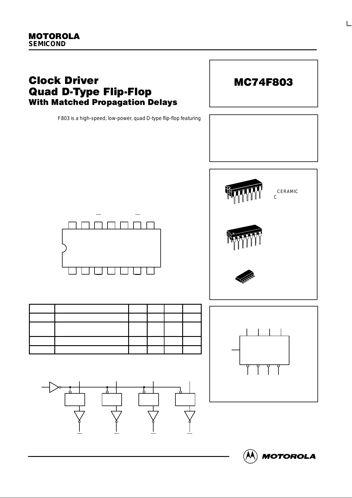
The MC74F803 is a high-speed, low-power, quad D-type flip-flop featuring
separate D-type inputs, and inverting outputs with closely matched
propagation delays. With a buffered clock (CP) input that is common to all
flip-flops, the F803 is useful in high-frequency systems as a clock driver,
providing multiple outputs that are synchronous. Because of the matched
propagation delays, the duty cycles of the output waveforms in a clock driver
application are symmetrical within 1.0 to 1.5 nanoseconds.
• Edge-Triggered D-Type Inputs
• Buffered Positive Edge-Triggered Clock
• Matched Outputs for Synchronous Clock Driver Applications
• Outputs Guaranteed for Simultaneous Switching
Pinout: 14-Lead Plastic (Top View)
14 13 12 11 10 9
123456
8
7
VCCNC O3
D3 D2 O2 CP
GND NC O0
D0 D1 O1 GND
GUARANTEED OPERATION RANGES
Symbol Parameter Min Typ Max Unit
V
CC
Supply Voltage 4.5 5.0 5.5 V
T
A
Operating Ambient
T emperature Range
0 25 70 °C
I
OH
Output Current — High — — –20 mA
I
OL
Output Current — Low — — 24 mA
LOGIC DIAGRAM
CP
D0
CP D
Q
O0
D1
CP D
Q
O1
D2
CP D
Q
O2
D3
CP D
Q
O3
CLOCK DRIVER QUAD
D-TYPE FLIP-FLOP WITH
MATCHED PROPAGATION
DELAYS
J SUFFIX
CERAMIC
CASE 632-08
N SUFFIX
PLASTIC
CASE 646-06
14
1
14
1
14
1
D SUFFIX
SOIC
CASE 751A-03
LOGIC SYMBOL
8
451011
36912
D0 D1 D2 D3
O1O0 O2 O3
CP
VCC = PIN 14
GND = PINS 1 AND 7
NC = PINS 2 AND 13
Page 2
MC74F803
2
MOTOROLA TIMING SOLUTIONS
BR1333 — REV 4
FUNCTIONAL DESCRIPTION
The F803 consists of four positive edge-triggered flip-flops
with individual D-type inputs and inverting outputs. The
buffered clock is common to all flip-flops and the following
specifications allow for outputs switching simultaneously. The
four flip-flops store the state of their individual D inputs that
meet the setup and hold time requirements on the
LOW-to-HIGH Clock (CP) transition. The maximum frequency
of the clock input is 70 megahertz, and the LOW-to-HIGH and
HIGH-to-LOW propagation delays of the O
1
output vary by, at
most, 1 nanosecond. Therefore, the device is ideal for use as
a divide-by-two driver for high-frequency clock signals that
require symmetrical duty cycles. The difference between the
LOW-to-HIGH and HIGH-to-LOW propagation delays for the
O
0
, O2, and O3 outputs vary by at most 1.5 nanoseconds.
These outputs are very useful as clock drivers for circuits with
less stringent requirements. In addition, the output-to-output
skew is a maximum of 1.5 nanoseconds. Finally, the I
OH
specification at 2.5 volts is guaranteed to be at least – 20
milliamps. If their inputs are identical, multiple outputs can be
tied together and the IOH is commensurately increased.
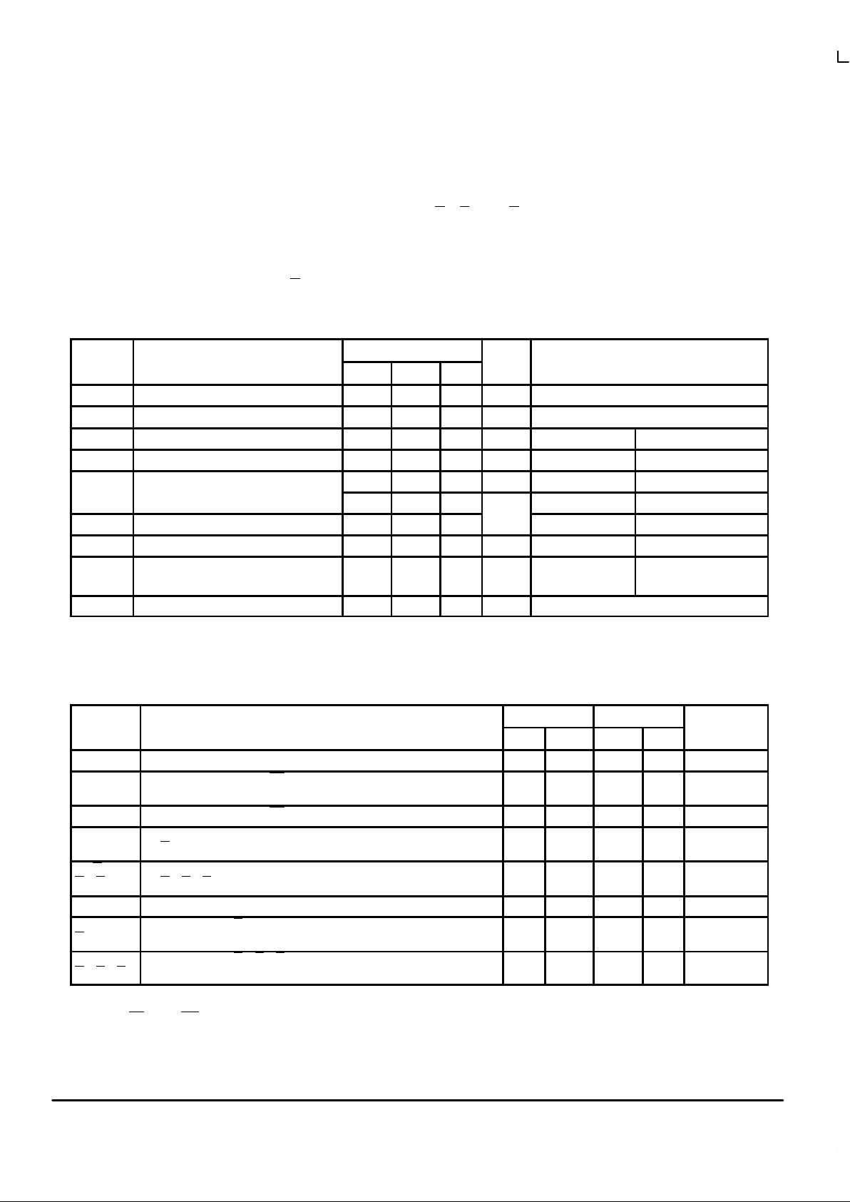
DC CHARACTERISTICS OVER OPERATING TEMPERATURE RANGE
(unless otherwise specified)
Limits
Symbol Parameter
Min Typ Max
Unit Test Conditions*
V
IH
Input HIGH Voltage 2.0 — — V Guaranteed Input HIGH Voltage
V
IL
Input LOW Voltage — — 0.8 V Guaranteed Input LOW Voltage
V
IK
Input Clamp Diode Voltage — — – 1.2 V IIN = –18 mA VCC = MIN
V
OH
Output HIGH Voltage 2.5 — — V IOH = –20 mA VCC = 4.5 V
V
OL
Output LOW Voltage
— 0.35 0.5 V IOL = 24 mA VCC = MIN
— — 20
µA
VIN = 2.7 V VCC = MAX
I
IH
Input HIGH Current — — 100 VIN = 7.0 V VCC = MAX
I
IL
Input LOW Current — — –0.6 mA VIN = 0.5 V VCC = MAX
I
OS
Output Short Circuit Current
(Note 2)
–60 — –150 mA V
OUT
= 0 V VCC = MAX
I
CC
Power Supply Current — — 70 mA VCC = MAX
* Normal test conditions for this device are all four outputs switching simultaneously. Two outputs of the 74F803 can be tied together and the
IOH doubles.
1. For conditions such as MIN or MAX, use the appropriate value specified under guaranteed operating ranges.
2. Not more than one output should be shorted at a time, nor for more than 1 second.
AC CHARACTERISTICS (T
A
= 0 to 70°C, VCC = 5.0 V ± 10%, see Note 1)
CL = 50 pF CL = 100 pF
Symbol Parameter
Min Max Min Max
Unit
f
max
Maximum Clock Frequency 70 — 50 — MHz
t
PLH
t
PHL
Propagation Delay CP to On 3.0 7.5 3.0 10 ns
t
Pv
Propagation Delay CP to On Variation (see Note 3) — 3.0 — 4.0 ns
tps O
1
Propagation Delay Skew |t
PLH
Actual – t
PHL
Actual|
for O
1
Only
— 1.0 — 2.0 ns
tps O0,
O
2
, O
3
Propagation Delay Skew |t
PLH
Actual – t
PHL
Actual|
for O
0
, O2, O
3
— 1.5 — 2.0 ns
t
os
Output to Output Skew (see Note 2) |tp On – tp Om| — 1.5 — 2.5 ns
t
rise
, t
fall
O
1
Rise/Fall Time for O1 (0.8 to 2.0 V) — 3.0 — 4.0 ns
t
rise
, t
fall
O
0
, O2, O
3
Rise/Fall Time for O0, O2, O3 (0.8 to 2.0 V) — 3.5 — 4.5 ns
1. The test conditions used are all four outputs switching simultaneously. The AC characteristics described above (except for O
1
) are also
guaranteed when two outputs are tied together.
2. Where tp On
and tp Om are the actual propagation delays (any combination of high or low) for two separate outputs from a given high
transition of CP.
3. For a given set of conditions (i.e., capacitive load, temperature, VCC, and number of outputs switching simultaneously) the variation from
device to device is guaranteed to be less than or equal to the maximum.
Page 3

MC74F803
3
MOTOROLATIMING SOLUTIONS
BR1333 — REV 4
AC OPERATING REQUIREMENTS (T
A
= 0 to 70°C, VCC = 5.0 V ± 10%)
CL = 50 pF CL = 100 pF
Symbol Parameter
Min Max Min Max
Unit
t
s(H)
t
s(L)
Setup Time, HIGH or LOW
Dn to CP
3.0
3.0
—
—
4.0
4.0
—
—
ns
t
f
tp + ts (see Note) — 9.0 — 12 ns
t
h(H)
t
h(L)
Hold Time, HIGH or LOW
Dn to CP
2.0
2.0
—
—
2.0
2.0
—
—
ns
t
w(H)
t
w(L)
CP Pulse Width
HIGH or LOW
7.0
6.0
—
—
8.0
8.0
—
—
ns
The combination of the setup time (ts) requirement and maximum propagation delay (tp) are guaranteed to be within this limit for all conditions.
APPLICATION NOTE
The closely matched outputs of the MC74F803 provide an ideal interface for the clock input of Motorola’s high-frequency
microprocessors.
74F803 INTERFACE AS CLOCK TO MC68020 SYSTEM
V
CC
33CLK1
E1
C2
MC68020/MC68030
CLK
CLK
MC68881/MC68882
R
U
R
T
33CLK
33CLK2 (40 mA OUTPUT DRIVE)
3
6
9
12
7
8
66 MHz
CLK
4
5
10
11
1
14
74F04
1
MC74F803
D0
D1
D2
D3
O0
O1
O2
O3
CP
2
V
CC
Page 4

MC74F803
4
MOTOROLA TIMING SOLUTIONS
BR1333 — REV 4
OUTLINE DIMENSIONS
N SUFFIX
PLASTIC PACKAGE
CASE 646-06
MIN MINMAX MAX
MILLIMETERS INCHES
DIM
18.16
6.10
3.69
0.38
1.02
1.32
0.20
2.92
19.56
6.60
4.69
0.53
1.78
2.41
0.38
3.43
0
°
0.39
0.715
0.240
0.145
0.015
0.040
0.052
0.008
0.115
0.770
0.260
0.185
0.021
0.070
0.095
0.015
0.135
10
°
1.01
2.54 BSC
7.62 BSC
0.100 BSC
0.300 BSC
0
°
0.015
10
°
0.039
A
B
C
D
F
G
H
J
K
L
M
N
NOTES:
1. LEADS WITHIN 0.13 mm (0.005) RADIUS OF TRUE
POSITION AT SEATING PLANE AT MAXIMUM
MATERIAL CONDITION.
2. DIMENSION “L” TO CENTER OF LEADS WHEN
FORMED PARALLEL.
3. DIMENSION “B” DOES NOT INCLUDE MOLD
FLASH.
4. ROUNDED CORNERS OPTIONAL.
5. 646-05 OBSOLETE, NEW STANDARD 646-06.
17
14 8
B
A
NOTE 4
F
H
G
D
SEATING
PLANE
N
K
C
L
J
M
D SUFFIX
SOIC PACKAGE
CASE 751A-02
MIN MINMAX MAX
MILLIMETERS INCHES
DIM
A
B
C
D
F
G
J
K
M
P
R
8.55
3.80
1.35
0.35
0.40
0.19
0.10
0
5.80
0.25
8.75
4.00
1.75
0.49
1.25
0.25
0.25
7
6.20
0.50
0.337
0.150
0.054
0.014
0.016
0.008
0.004
0
0.229
0.010
0.344
0.157
0.068
0.019
0.049
0.009
0.009
7
0.244
0.019
1.27 BSC 0.050 BSC
°°
°
°
NOTES:
1. DIMENSIONS “A” AND “B” ARE DATUMS AND
“T” IS A DATUM SURFACE.
2. DIMENSIONING AND TOLERANCING PER ANSI
Y14.5M, 1982.
3. CONTROLLING DIMENSION: MILLIMETER.
4. DIMENSION A AND B DO NOT INCLUDE MOLD
PROTRUSION.
5. MAXIMUM MOLD PROTRUSION 0.15 (0.006)
PER SIDE.
6. 751A-01 IS OBSOLETE, NEW STANDARD
751A-02.
0.25 (0.010)MT
SS
A
B
MM
0.25 (0.010) B
-A-
-B-
P
G
C
K
SEATING
PLANE
14 PL
D
M
F
J
7 PL
R X 45°
1
7
814
J SUFFIX
CERAMIC PACKAGE
CASE 632-08
MIN MINMAX MAX
MILLIMETERS INCHES
DIM
A
B
C
D
F
G
J
K
L
M
N
19.05
6.23
3.94
0.39
1.40
0.21
3.18
0
0.51
19.94
7.11
5.08
0.50
1.65
0.38
4.31
15
1.01
0.750
0.245
0.155
0.015
0.055
0.008
0.125
0
0.020
0.785
0.280
0.200
0.020
0.065
0.015
0.170
15
0.040
°°°
°
2.54 BSC
7.62 BSC
0.100 BSC
0.300 BSC
NOTES:
1. DIMENSIONING AND TOLERANCING PER ANSI
Y14.5M, 1982.
2. CONTROLLING DIMENSION: INCH.
3. DIMENSION L TO CENTER OF LEAD WHEN
FORMED PARALLEL.
4. DIM F MAY NARROW TO 0.76 (0.030) WHERE
THE LEAD ENTERS THE CERAMIC BODY.
5. 632-01 THRU -07 OBSOLETE, NEW STANDARD
632-08.
14 8
17
-A-
-B-
-T-
SEATING
PLANE
FG
D
14 PL
N
K
C
L
J
14 PL
M
0.25 (0.010)MTSA
0.25 (0.010)MTSB
Page 5

MC74F803
5
MOTOROLATIMING SOLUTIONS
BR1333 — REV 4
Motorola reserves the right to make changes without further notice to any products herein. Motorola makes no warranty , representation or guarantee regarding
the suitability of its products for any particular purpose, nor does Motorola assume any liability arising out of the application or use of any product or circuit,
and specifically disclaims any and all liability, including without limitation consequential or incidental damages. “T ypical” parameters can and do vary in different
applications. All operating parameters, including “T ypicals” must be validated for each customer application by customer’s technical experts. Motorola does
not convey any license under its patent rights nor the rights of others. Motorola products are not designed, intended, or authorized for use as components in
systems intended for surgical implant into the body, or other applications intended to support or sustain life, or for any other application in which the failure of
the Motorola product could create a situation where personal injury or death may occur. Should Buyer purchase or use Motorola products for any such
unintended or unauthorized application, Buyer shall indemnify and hold Motorola and its officers, employees, subsidiaries, affiliates, and distributors harmless
against all claims, costs, damages, and expenses, and reasonable attorney fees arising out of, directly or indirectly, any claim of personal injury or death
associated with such unintended or unauthorized use, even if such claim alleges that Motorola was negligent regarding the design or manufacture of the part.
Motorola and are registered trademarks of Motorola, Inc. Motorola, Inc. is an Equal Opportunity/Affirmative Action Employer .
Literature Distribution Centers:
USA: Motorola Literature Distribution; P.O. Box 20912; Phoenix, Arizona 85036.
EUROPE: Motorola Ltd.; European Literature Centre; 88 Tanners Drive, Blakelands, Milton Keynes, MK14 5BP, England.
JAPAN: Nippon Motorola Ltd.; 4-32-1, Nishi-Gotanda, Shinagawa-ku, Tokyo 141 Japan.
ASIA-PACIFIC: Motorola Semiconductors H.K. Ltd.; Silicon Harbour Center, No. 2 Dai King Street, Tai Po Industrial Estate,
ASIA-PACIFIC: Tai Po, N.T., Hong Kong.
◊
CODELINE TO BE PLACED HERE
MC74F803/D
*MC74F803/D*
 Loading...