

Page 1
HI-SINCERITY
MICROELECTRONICS CORP.
H1117J Series
1A LOW DROPOUT POSITIVE VOLTAGE REGULATOR
Features
•
Low Dropout Voltage 1.2V at 1A
•
Adjustable or Fixed Voltage
•
Maximum Line Regulation 0.45%
•
Maximum Load Regulation 0.4%
•
Adjust Pin Current Less Than 90 uA
•
Over Current Protection
•
Thermal Protection
Applications
•
High Efficiency Linear Regulators
•
5V to 3.3V Voltage Converter
•
Battery Charger
Spec. No. : Preliminary Data
Issued Date : 1998.06.01
Revised Date : 2000.10.01
Page No. : 1/6
General Description
The H1117J is a 1A low-dropout positive voltage regulator. It is available in fixed and adjustable output voltage
versions. Over curre nt and thermal protection are integr ated onto the chip. Output current will decr ease while it
reaches the pre-set current or tem perature limit. The dropout voltage is specified at 1.2V Maximum at full rated
output current. H1117J Series provides excellent regulation over variations due to changes in line, load and
temperature. H1117J is three terminal regulator and available in popular packages.
Device Selection Guide
Device Output Voltage Package
H1117J(Adj) 1.3V to 4V
H1117-3.3J 3.3
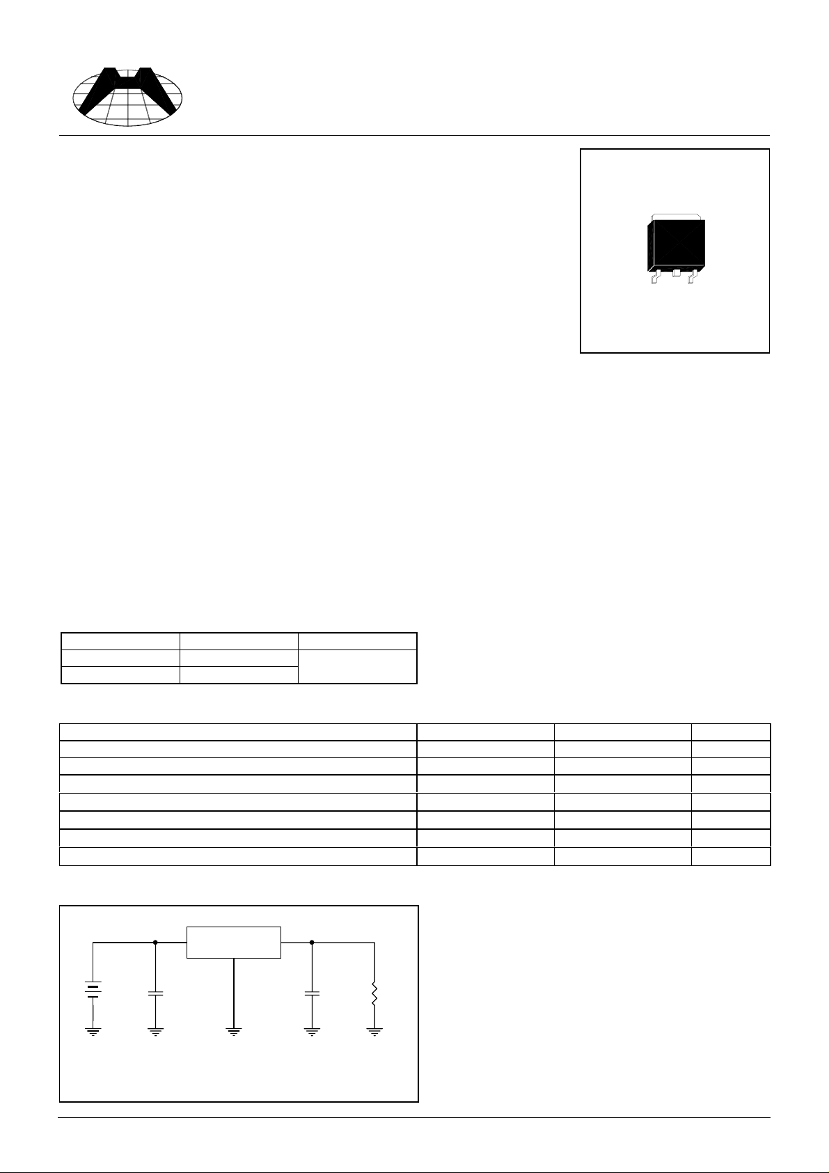
D-PAK
TO-252
Absolute Maximum Ratings
Parameter Symbol Maximum Units
Input Voltage V
Power Dissipation P
Thermal Resistance Junction To Case TO-252
Thermal Resistance Junction To Ambient TO-252
Operating Junction Temperature Range T
Storage Temperature Range T
Lead Temperature (Soldering) 10 Sec T
θ
θ
IN
D
JC
JA
j
STG
LEAD
Internally Limited W
20 V
15
156
0 To 125
-65 To 150
260
°
C/W
°
C/W
°
°
°
C
C
C
Typical Application
H1117J
+
4.75V
to 20V
DC
Input Range Depends On V
Please Refer To Electrical Characteristics.
10uF
TAN
GND
O
10uF
TAN
Load
HSMC Product Specification
Page 2
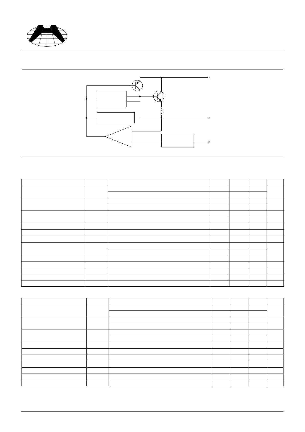
Block Diagram
HI-SINCERITY
MICROELECTRONICS CORP.
Current
Limiting
Amplifier
Spec. No. : Preliminary Data
Issued Date : 1998.06.01
Revised Date : 2000.10.01
Page No. : 2/6
Input
Electrical Characteristics
H1117J (adj version)
Parameter Symbol Test Conditions Min Typ Max Units
Reference Voltage V
Line Regulation Reg
Load Regulation Reg
Dropout Voltage V
Current Limit I
Temperature Coeff. T
Adjust Pin Current I
Adjust Pin Current Change
Temperature Stability T
Minimum Load Current I
RMS Output Noise V
Ripple Rejection Ratio R
∆
REF
LINE
LOAD
D
S
C
adj
I
adj
S
O
N
A
Thermal
Protection
Error
AMP
VIN=5V, IO=10mA, Tj=25°C
Bandcap
Reference
Output
ADJ/COM
1.238 1.25 1.262
VIN=5V, IO=10mA, Over Temp. 1.225 1.25 1.275
VIN=4.75~20V, IO=10mA, Tj=25°C
--0.3
VIN=4.75~20V, IO=10mA, Over Temp. - - 0.45
VIN=5V, IO=10mA~1A,Tj=25°C
- 0.05 0.3
VIN=5V, IO=10mA~1A, Over Temp. - 0.2 0.4
IO=10mA~1A, Over Temp., ∆VO=±1%
-11.2V
VIN=2.75~7V, Over Temp. 1 - - A
VIN=2.75~7V, IO=10mA~1A - 0.005 VIN=2.75~7V, IO=10mA~1A,Tj=25°C
-55VIN=2.75~7V, IO=10mA~1A, Over Temp. - - 90
VIN=2.75~7V, IO=10mA~1A, Over Temp. - 0.2 5
VIN=5V, IO=100mA, Over Temp. - 0.5 - %
VIN=5V - 5 10 mA
Tj=25°C
-0.003- %
VIN=5V, IO=1A, Over Temp. 60 72 - dB
V
%
%
%/°C
uA
H1117-3.3J
Parameter Symbol Test Conditions Min Typ Max Units
Output Voltage V
Line Regulation Reg
Load Regulation Reg
Dropout Voltage V
Current Limit I
Quiescent Current I
Temperature Coeff. T
Temperature Stability T
RMS Output Noise V
Ripple Rejection Ratio R
VIN=5V, IO=0A,Tj=25°C
O
VIN=5V, IO=0A, Over Temp. 3.234 3.3 3.366
VIN=4.75~20V, IO=0A, Tj=25°C
LINE
VIN=4.75~20V, IO=0A, Over Temp. - - 0.45
VIN=5V, IO=0A~1A,Tj=25°C
LOAD
VIN=5V, IO=0A~1A, Over Temp. - 0.2 0.4
IO=0A~1A, Over Temp., ∆VO=±1%
D
VIN=4.75~7V, Over Temp. 1 - - A
S
VIN=5V, IO=0A~1A,Over Temp. - 12 13 mA
Q
VIN=4.75~7V, IO=0A~1A - 0.005 -
C
VIN=5V, IO=100mA, Over Temp. - 0.5 - %
S
Tj=25°C
N
VIN=5V, IO=1A, Over Temp. 60 72 - dB
A
3.270 3.3 3.333
--0.3
- 0.05 0.3
-11.2V
-0.003- %
HSMC Product Specification
V
%
%
%/°C
Page 3

HI-SINCERITY
MICROELECTRONICS CORP.
Characteristics Curve
Spec. No. : Preliminary Data
Issued Date : 1998.06.01
Revised Date : 2000.10.01
Page No. : 3/6
Load Regu la tion
0
-0.05
-0.1
-0.15
Output Voltage deviation (%)
-0.2
-0.25
-50 -40 -30 -20 -10 0 10 20 30 40 50 60 70 80 90 100
Tem per atur e ( ºC)
Minimum O perating Cu rrent
3.5
3
2.5
2
1.5
1
0.5
Minimum Operating Current (mA)
0
-0.5
0 0.1 1 1.1 1.2 2 3 5 10 15 20 25 30 35
In put /Outpu t Differential (V)
1.252
1.25
1.248
1.246
1.244
Referen ce Voltage ( V)
1.242
1.24
1.238
-50 -25 0 25 50 75 100 125
Tem per atur e (º C)
Ajust Pin Current
45
40
35
30
25
20
15
Adjust Pin Current ( uA)
10
5
0
Temperature Stability
-50 -25 0 25 50 75 100 125
Temperatu re (ºC)
1.6
Short Circuit Current
1.4
1.2
1
0.8
0.6
Short Circuit Current (A)
0.4
0.2
0
1.2 1.3 1.5 1.7 2 5 10 15
In put/Outpu t Differential (V)
1.4
1.2
1
0.8
0.6
0.4
Minmum Input/Ou tput Differential (V)
0.2
0
0.1 0.3 0.5 0.7 0.9 1
Output Current (A)
HSMC Product Specification
Dropout Voltage
Page 4

HI-SINCERITY
MICROELECTRONICS CORP.
Spec. No. : Preliminary Data
Issued Date : 1998.06.01
Revised Date : 2000.10.01
Page No. : 4/6
Applications Description
Output Voltage Adjustment
•
Like most regulators, the H1117J regulates the output by
comparing the output voltage to an internally generated
reference voltage. On the adjustable version, the V
available externally as 1.25V between V
voltage ratio formed by R
and R2 should be set to conduct
1
and ADJ. The
OUT
REF
is
V
IN
10mA (minimum output load). The output voltage is given
=V
by the following equation : V
OUT
(1+R2/R1) + I
REF
ADJ R2
On fixed versions of H1117J, the voltage divider is
provided internally.
Thermal Protection
•
H1117J has thermal protection which limits junction
temperature to 150°C. However, device functionality is
only guaranteed to a maximum junction temperature of
+125°C.
The power dissipation and junction temperature for H1117J in TO-252 package given by
=(V
- V
) I
P
D
IN
OUT
Current Limit Protection
•
, T
OUT
JUNCTION=TAMBIENT
+(PDx
θ
), Note : T
JA
JUNCTION
must not exceed 125°C
H1117J is protected against overload conditions. Current protection is triggered at typically 1.5A.
In
I
ADJ
10uA
V
=V
OUT
REF
Out
ADJ
(1+R2/R1) + I
V
REF
ADJ R2
R1
R2
V
OUT
Stability And Load Regu lation
•
H1117J requires a capacitor from V
compensation feedback to the internal gain stage. This is
to ensure stability at the output terminal. Typically, a 10uF
tantalum or 50uF aluminum electrolytic is sufficient.
Note : It is important that the ESR for this capacitor does
not exceed 0.5Ω.
The output capacitor does not have a theoretical upper
limit and increasing its va lue wi ll inc reas e st abi l it y. C
to GND to provide
OUT
OUT
=
R
P
Parasitic
Line Resistance
OutIn
V
IN
Adj
R1
R2
Connect
R1 to Case
RL
100 uF or more is typical for high current regulator design.
H1117J load regulation is limited by the resistance of the
wire connecting it to the load(R
version, the best load regulation is accomplished when the
top of the resistor divider(R
output pin of the H1117J. When so connected, R
). For the adjustable
P
) is connected directly to the
1
is not
P
Connect
R2 to Load
multiplied by the divider ratio. For fixed output versions,
the top of R
is internally connected to the output and ground pin can be connected to low side of the load as a
1
negative side sense if, so desired.
Thermal Consideration
•
The H1117J series contain thermal limiting circuitry designed to protect itself for over-temperature conditions.
Even for normal load conditions, maximum junction temperature ratings must not be exceeded. As mention in
thermal protection section, we need to consider all sources of thermal resistance between junction and ambient.
It contains junction-to-case, case-to-heat-sink interface and heat sink resistance itself. An additional heat sink is
applied externally sometimes. It can increase the maximum power dissipation. For example, the equivalent
junction temperature of 300mA output current is 115°C without external heat sink. Under the same junction
temperature IC can operates 500mA with an adequate heat sink. Therefore, to attach an extra heat sink is
recommended.
Junction-to-case thermal resistance is specified from the IC junction to the bottom of the case directly below the
die. The bonding wires are appending paths. The former is the lowest resistance path. Proper mounting is
required to ensure the best possible thermal flow this area of the package to the heat sink. Thermal compound at
the case-to-heat-sink interface is strongly recommended. The case of all devices in this series is electrically
connected to the output. Therefore, if the case of the device must be electrically isolated, a thermally conductive
spacer can be used, as long its thermal resistance is considered.
HSMC Product Specification
Page 5

HI-SINCERITY
MICROELECTRONICS CORP.
Protection Diode
•
(The figure is shown as Regulator with Reverse Diode Protection in advanced applications)
In general operation, H1117J does not need any protection diodes. From the cross-section structure of H1117J,
the output pin is connected to P+ substrate, and the input pin is connected to N- well. There is a parasitic reverse
diode between them. It can handle microsecond surge currents of 5A to 10A. Even with large output capacitance,
it is very difficult to get those values of surge currents in normal operation. Only with high value output capacitors,
such as 1000uF. And with the input pin instantaneously shorted to ground. can damage occur. A crowbar circuit
at the input of the H1117J can generate those kinds of currents, and a diode from output to input is
recommended. Normal power supply cycling or even plugging and unplugging in the system will not generate
currents large enough to do any damage.
Spec. No. : Preliminary Data
Issued Date : 1998.06.01
Revised Date : 2000.10.01
Page No. : 5/6
HSMC Product Specification
Page 6

HI-SINCERITY
MICROELECTRONICS CORP.
TO-252 Dimension
Spec. No. : Preliminary Data
Issued Date : 1998.06.01
Revised Date : 2000.10.01
Page No. : 6/6
A
B
L
F
G
C
D
Marking :
HSMC Logo
Part Number
Date Code
Product Series
Rank
Ink Mark
Style : Pin 1.COM/ADJ 2.Vout 3.Vin
3
H
E
K
2
I
1
J
3-Lead TO-252 Plastic Surface Mount Package
HSMC Package Code : J
DIM
Inches Millimeters Inches Millimeters
Min. Max. Min. Max.
DIM
Min. Max. Min. Max.
A 0.0177 0.0217 0.45 0.55 G 0.0866 0.1102 2.20 2.80
B 0.0650 0.0768 1.65 1.95 H - *0.0906 - *2.30
C 0.0354 0.0591 0.90 1.50 I - 0 .0354 - 0.90
D 0.0177 0.0236 0.45 0.60 J - 0 .0315 - 0.80
E 0.2520 0.2677 6.40 6.80 K 0.2047 0.2165 5.20 5.50
F 0.2125 0.2283 5.40 5.80 L 0.0551 0.0630 1.40 1.60
Notes :
Material :
• Lead : 42 Alloy ; solder plating
• Mold Compound : Epoxy resin family, flammability solid burning class:UL94V-0
1.Dimension and tolerance based on our Spec. dated May. 05,1996.
2.Controlling dimension : millimeters.
3.Maximum lead thickness includes lead finish thickness, and minimum lead thickness is the minimum thickness of base material.
4.If there is any question with packing specification or packing method, pleas e contact your l ocal HSMC sal es office.
*:Typical
Important Notice:
• All rights are reserved. Reproduction in whole or in part is prohibited without the prior written approval of HSMC.
• HSMC reserves the right to make changes to its products without notice.
•
HSMC semiconductor products are not warranted to be suitable for use in Life-Support Applications, or systems.
• HSMC assumes no liability for any consequence of customer product design, infringem ent of pat ents, or applic ati on assistance.
Head Office And Factory :
•
Head Office
Tel : 886-2-25212056 Fax : 886-2-25632712, 25368454
•
Factory 1 :
Tel : 886-3-5983621~5 Fax : 886-3-5982931
•
Factory 2 :
Tel : 886-3-5977061 Fax : 886-3-5979220
(Hi-Sincerity Microelectronics Corp.) : 10F.,No. 61, Sec. 2, Chung-Shan N. Rd. Taipei Taiwan R.O.C.
No. 38, Kuang Fu S. Rd., Fu-Kou Hsin-Chu Industrial Park Hsin-Chu Taiwan. R.O.C
No. 17-1, Ta-Tung Rd., Fu-Kou Hsin-Chu Industrial Park Hsin-Chu Taiwan. R.O.C
HSMC Product Specification
 Loading...