

Page 1
HI-SINCERITY
MICROELECTRONICS CORP.
H1117E Series
1A LOW DROPOUT POSITIVE VOLTAGE REGULATOR
Features
•
Low Dropout Voltage 1.2V at 1A
•
Adjustable or Fixed Voltage
•
Maximum Line Regulation 0.45%
•
Maximum Load Regulation 0.4%
•
Adjust Pin Current Less Than 90 uA
•
Over Current Protection
•
Thermal Protection
Applications
•
High Efficiency Linear Regulators
•
5V to 3.3V Voltage Converter
•
Battery Charger
Spec. No. : Preliminary Data
Issued Date : 1998.07.15
Revised Date : 1999.08.01
Page No. : 1/4
General Description
The H1117E is a 1A low-dropout positive voltag e regulator. It is available in fixed and adjustable output v oltage
versions. Over curre nt and thermal protection are integr ated onto the chip. Output current will decr ease while it
reaches the pre-set current or tem perature limit. The dropout voltage is specified at 1.2V Maximum at full rated
output current. H1117E Series provides excellent regulation over variations due to changes in line, load and
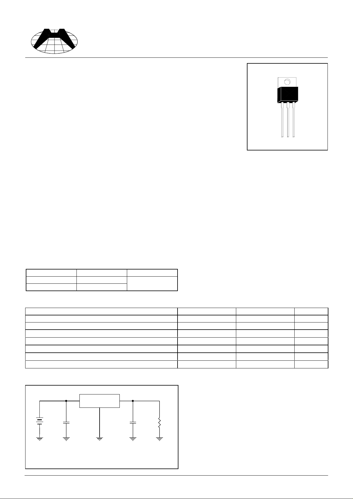
temperature. H1117E is three terminal regulator and available in popular packages.
Device Selection Guide
Device Output Voltage Package
H1117E(Adj) 1.3V to 4V
H1117-3.3E 3.3
TO-220AB
Absolute Maximum Ratings
Parameter Symbol Maximum Units
Input Voltage V
Power Dissipation P
Thermal Resistance Junction To Case TO-220AB
Thermal Resistance Junction To Ambient TO-220AB
Operating Junction Temperature Range T
Storage Temperature Range T
Lead Temperature (Soldering) 10 Sec T
θ
θ
IN
D
JC
JA
j
STG
LEAD
Internally Limited W
20 V
3
50
0 To 125
-65 To 150
260
°
C/W
°
C/W
°
°
°
C
C
C
Typical Application
H1117E
+
4.75V
to 20V
DC
Input Range Depends On V
Please Refer To Electrical Characteristics.
10uF
TAN
GND
O
10uF
TAN
Load
HSMC Product Specification
Page 2
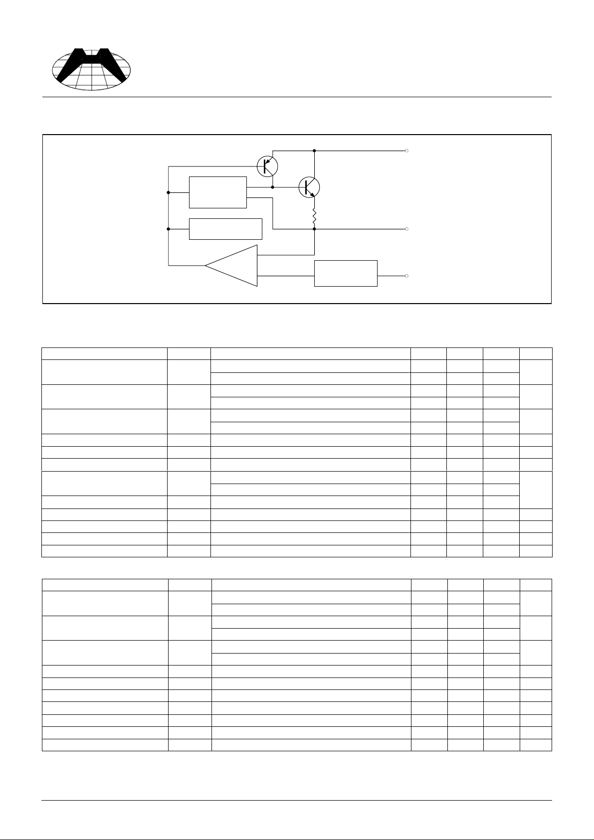
Block Diagram
HI-SINCERITY
MICROELECTRONICS CORP.
Current
Limiting
Amplifier
Spec. No. : Preliminary Data
Issued Date : 1998.07.15
Revised Date : 1999.08.01
Page No. : 2/4
Input
Electrical Characteristics
H1117E (adj version)
Parameter Symbol Test Conditions Min Typ Max Units
Reference Voltage V
Line Regulation Reg
Load Regulation Reg
Dropout Voltage V
Current Limit I
Temperature Coeff. T
Adjust Pin Current I
Adjust Pin Current Change
Temperature Stability T
Minimum Load Current I
RMS Output Noise V
Ripple Rejection Ratio R
∆
REF
LINE
LOAD
D
S
C
adj
I
adj
S
O
N
A
Thermal
Protection
Error
AMP
VIN=5V, IO=10mA, Tj=25°C
Bandcap
Reference
Output
ADJ/COM
1.238 1.25 1.262
VIN=5V, IO=10mA, Over Temp. 1.225 1.25 1.275
VIN=4.75~20V, IO=10mA, Tj=25°C
--0.3
VIN=4.75~20V, IO=10mA, Over Temp. - - 0.45
VIN=5V, IO=10mA~1A,Tj=25°C
- 0.05 0.3
VIN=5V, IO=10mA~1A, Over Temp. - 0.2 0.4
IO=10mA~1A, Over Temp., ∆VO=±1%
-11.2V
VIN=2.75~7V, Over Temp. 1 - - A
VIN=2.75~7V, IO=10mA~1A - 0.005 VIN=2.75~7V, IO=10mA~1A,Tj=25°C
-55VIN=2.75~7V, IO=10mA~1A, Over Temp. - - 90
VIN=2.75~7V, IO=10mA~1A, Over Temp. - 0.2 5
VIN=5V, IO=100mA, Over Temp. - 0.5 - %
VIN=5V - 5 10 mA
Tj=25°C
-0.003- %
VIN=5V, IO=1A, Over Temp. 60 72 - dB
V
%
%
%/°C
uA
H1117-3.3E
Parameter Symbol Test Conditions Min Typ Max Units
Output Voltage V
Line Regulation Reg
Load Regulation Reg
Dropout Voltage V
Current Limit I
Quiescent Current I
Temperature Coeff. T
Temperature Stability T
RMS Output Noise V
Ripple Rejection Ratio R
VIN=5V, IO=0A,Tj=25°C
O
VIN=5V, IO=0A, Over Temp. 3.234 3.3 3.366
VIN=4.75~20V, IO=0A, Tj=25°C
LINE
VIN=4.75~20V, IO=0A, Over Temp. - - 0.45
VIN=5V, IO=0A~1A,Tj=25°C
LOAD
VIN=5V, IO=0A~1A, Over Temp. - 0.2 0.4
IO=0A~1A, Over Temp., ∆VO=±1%
D
VIN=4.75~7V, Over Temp. 1 - - A
S
VIN=5V, IO=0A~1A,Over Temp. - 12 13 mA
Q
VIN=4.75~7V, IO=0A~1A - 0.005 -
C
VIN=5V, IO=100mA, Over Temp. - 0.5 - %
S
Tj=25°C
N
VIN=5V, IO=1A, Over Temp. 60 72 - dB
A
3.270 3.3 3.333
--0.3
- 0.05 0.3
-11.2V
-0.003- %
HSMC Product Specification
V
%
%
%/°C
Page 3

HI-SINCERITY
MICROELECTRONICS CORP.
Characteristics Curve
Spec. No. : Preliminary Data
Issued Date : 1998.07.15
Revised Date : 1999.08.01
Page No. : 3/4
0
-0.05
-0.1
-0.15
Output Voltage deviation (%)
-0.2
-0.25
-50 -40 -30 -20 -10 0 10 20 30 40 50 60 70 80 90 100
Tem per atur e ( ºC)
Minimum O perating Current
3.5
3
2.5
2
1.5
1
0.5
Minimum Operating Current (mA)
0
Load Regu la tion
1.252
1.25
1.248
1.246
1.244
Refer e nce Vol t age(V)
1.242
1.24
1.238
-50 -25 0 25 50 75 100 125
45
40
35
30
25
20
15
Adjust Pin Cur r ent (u A)
10
5
Temperature Stability
Tem per atur e ( ºC)
Aju st Pi n Cu rrent
-0.5
0 0.1 1 1.1 1.2 2 3 5 10 15 20 25 30 35
1.6
1.4
1.2
1
0.8
0.6
Sh ort Circuit Curren t (A )
0.4
0.2
0
1.2 1.3 1.5 1.7 2 5 10 15
In put / Output Differential (V)
Short Circuit Current
In put/Output Differential (V)
0
-50 -25 0 25 50 75 100 125
Tem per atur e ( ºC)
Dropout Voltage
1.4
1.2
1
0.8
0.6
0.4
Minmum Input/Ou tput Differential (V)
0.2
0
0.1 0.3 0.5 0.7 0.9 1
Output Current (A)
HSMC Product Specification
Page 4

HI-SINCERITY
MICROELECTRONICS CORP.
TO-220AB Dimension
A B
D
H
I
G
Spec. No. : Preliminary Data
Issued Date : 1998.07.15
Revised Date : 1999.08.01
Page No. : 4/4
Marking :
E
M
C
K
HSMC Logo
Part Number
Date Code
Product Series
Rank
Style : Pin 1.ADJ/COM 2.Vout 3.Vin
4.Vout
3
2
N
4
1
DIM
P
3-Lead TO-220AB Plastic Package
HSMC Package Code : E
Inches Millimeters Inches Millimeters
Min. Max. Min. Max.
O
DIM
Min. Max. Min. Max.
A 0.2197 0.2949 5.58 7.49 I - *0.1508 - *3.83
B 0.3299 0.3504 8.38 8.90 K 0.0295 0.0374 0.75 0.95
C 0.1732 0.185 4.40 4.70 M 0.0449 0.0551 1.14 1.40
D 0.0453 0.0547 1.15 1.39 N - *0.1000 - *2.54
E 0.0138 0.0236 0.35 0.60 O 0.5000 0.5618 12.70 14.27
G 0.3803 0.4047 9.66 10.28 P 0.5701 0.6248 14.48 15.87
H - *0.6398 - *16.25
Notes :
Material :
• Lead : 42 Alloy ; solder plating
• Mold Compound : Epoxy resin family, flammability solid burning class:UL94V-0
1.Dimension and tolerance based on our Spec. dated Sep. 07,1997.
2.Controlling dimension : millimeters.
3.Maximum lead thickness includes lead finish thickness, and minimum lead thickness is the minimum thickness of base material.
4.If there is any question with packing specification or packing method, pleas e contact your l ocal HSMC sal es office.
*:Typical
Important Notice:
• All rights are reserved. Reproduction in whole or in part is prohibited without the prior written approval of HSMC.
• HSMC reserves the right to make changes to its products without notice.
•
HSMC semiconductor products are not warranted to be suitable for use in Life-Support Applications, or systems.
• HSMC assumes no liability for any consequence of customer product design, infringem ent of pat ents, or applic ati on assistance.
Head Office And Factory :
•
Head Office
Tel : 886-2-25212056 Fax : 886-2-25632712, 25368454
•
Factory 1 :
Tel : 886-3-5983621~5 Fax : 886-3-5982931
•
Factory 2 :
Tel : 886-3-5977061 Fax : 886-3-5979220
(Hi-Sincerity Microelectronics Corp.) : 10F.,No. 61, Sec. 2, Chung-Shan N. Rd. Taipei Taiwan R.O.C.
No. 38, Kuang Fu S. Rd., Fu-Kou Hsin-Chu Industrial Park Hsin-Chu Taiwan. R.O.C
No. 17-1, Ta-Tung Rd., Fu-Kou Hsin-Chu Industrial Park Hsin-Chu Taiwan. R.O.C
HSMC Product Specification
 Loading...