

GY4102A Fast Toggling
Video Switch
DATA SHEET
FEATURES
• 20 ns switching time (toggle)
• make-before-break switching
• 100 MHz at
±0.1dB, bandwidth (flattened)
• typically 0.04 dB insertion loss at 1 MHz
• typically 0.03 % differential gain at 3.58 MHz
• typically 0.01 degree differential phase at 3.58 MHz
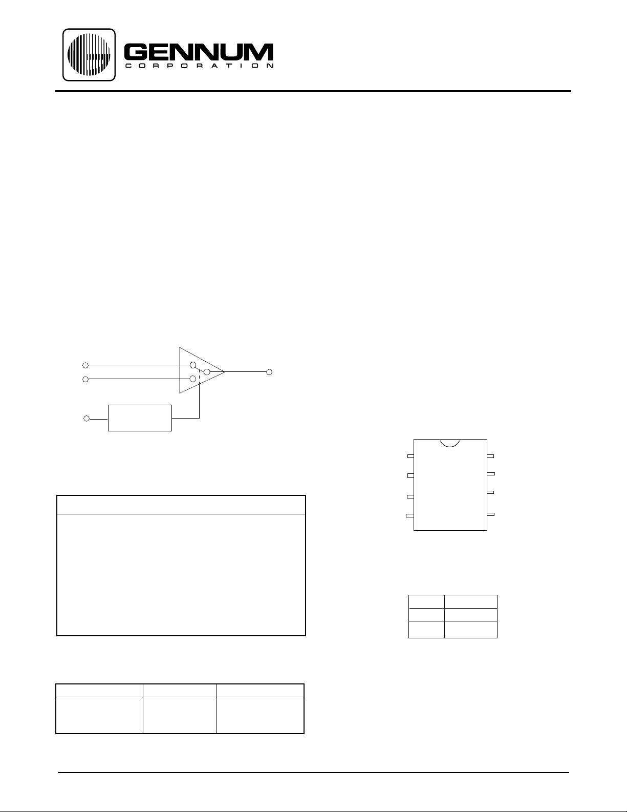
FUNCTIONAL BLOCK DIAGRAM
IN 0
IN 1
CTRL
CONTROL
LOGIC
OUT
CIRCUIT DESCRIPTION
The GY4102A is a bipolar, monolithic SPDT video switch
incorporating fast control logic. The analog signal path is
characterised by low differential gain, low differential phase
and low insertion loss, coupled with a ±0.1 dB bandwidth
of typically 100 MHz into a 10 pF load, using an external
series resistor.
In demanding video applications the GY4102A features a
typical switching glitch of less than 30 mV over a 3 ns
period. The device offers toggle rates up to 50 MHz. The
control input is TTL and 5 V CMOS compatible.
APPLICATIONS
• Sub-pixel video switching
• Fast data sampling
• Modulation
• Special Effects video switching
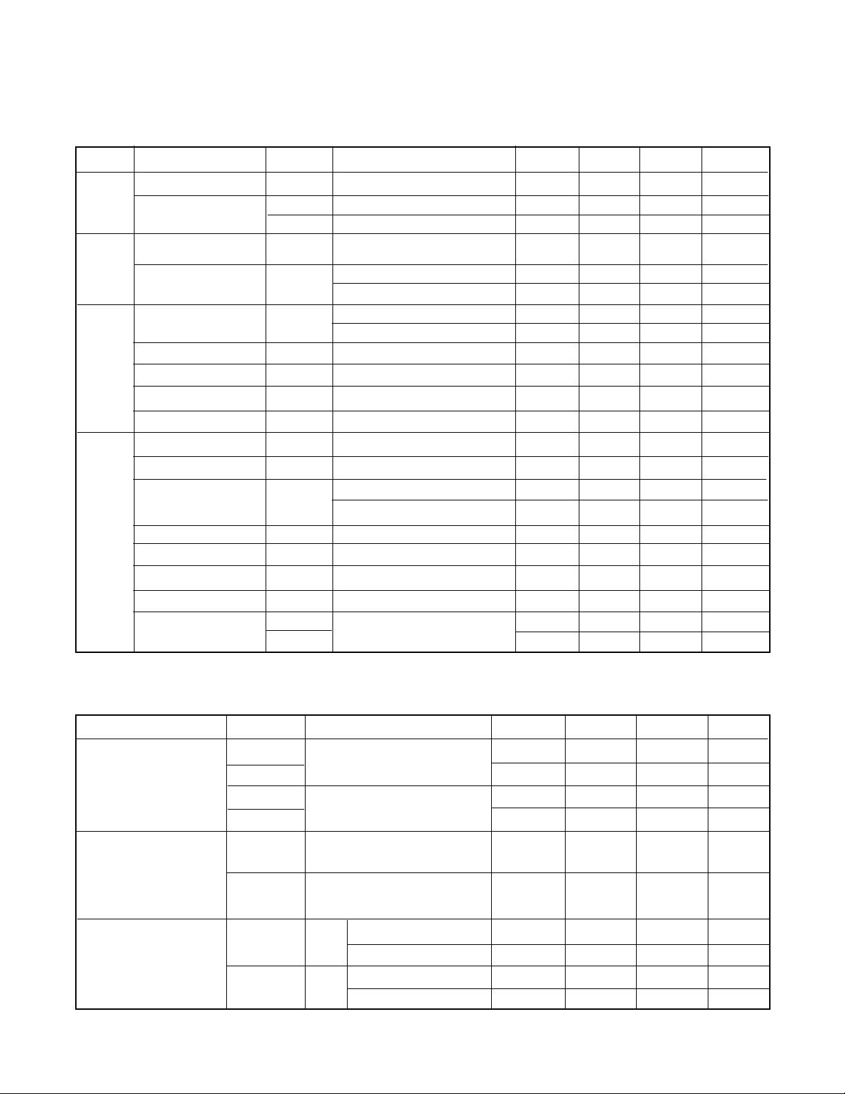
PIN CONNECTIONS
TOP VIEW
ABSOLUTE MAXIMUM RATINGS
PARAMETER VALUE
Supply Voltage ±6.0 V
Operating Temperature Range 0°C to 70° C
Storage Temperature Range -65°C to 150° C
Lead Temperature (Soldering, 10 Sec) 260° C
Analog Input Voltage (IN 0, IN 1) VEE <VIN <V
Control Input Voltage Range -5 V < V
CTRL
CC
< VCC+0.3 V
ORDERING INFORMATION
Part Number Package Type Temperature Range
GY4102ACDA 8 pin PDIP 0 - 70oC
GY4102ACKA 8 pin SOIC 0 - 70oC
+0.3 V
IN 0
GND 1
V
IN 1
PIN 1
EE
4
TRUTH TABLE
CTRL OUTPUT
0 IN 0
1 IN 1
AVAILABLE PACKAGING
• 8 pin PDIP
• 8 pin SOIC
8 PIN PDIP
8 PIN SOIC
8
CTRL
GND 2
OUT
V
5
CC
Document No. 520 - 21 - 2
GENNUM CORPORATION P.O. Box 489, Stn A, Burlington, Ontario, Canada L7R 3Y3 tel. (416) 632-2996 fax: (416) 632-2055 telex: 061-8525
Japan Branch: B-210 Miyamae Village, 2-10-42 Miyamae, Suginami-ku, Tokyo 168, Japan tel. (03) 3247-8838 fax: (03) 3247-8839
ELECTRICAL CHARACTERISTICS
PARAMETER SYMBOL CONDITIONS MIN TYP MAX UNITS
(V
= ±5V DC, TA = 0 - 70°C, CL = 10pF, RL = 10 kΩ unless otherwise shown)
S
Supply Voltage ±V
S
4.5 5 5.5 V
DC Supply Current I+ -2330mA
SUPPLY I- -2532mA
Control Input Bias I
LOGIC Logic Level threshold V
CTRL
LOGIC
Control = 1 - 5 25 µA
1 2 - - V
0 - - 0.8 V
Analog Input I
BIAS
Selected channel - 12 30 µA
Bias Current Deselected channel - 26 60 µA
Signal Voltage Swing V
STATIC Output Offset Voltage V
Output Offset Voltage V
SIG
OS
OSCH-CHTA
Extremes before clipping occurs -1.5 - +3 V
TA = 25°C -6 +4 +14 mV
= 25°C channel to channel - 1 5 mV
Output Offset Drift ∆VOS/T - +93 +200 µV/°C
Input Resistance R
Input Capacitance C
IN
IN
Channel On 500 - - kΩ
Channel On 1.3 - - pF
Frequency Response DC - 100 MHz RS = 33 Ω - ± 0.2 - dB
DYNAMIC Flatness DC - 8 MHz RS = 33 Ω - - ± 0.01 dB
Insertion Loss I.L. ƒ = 1 MHz - 0.04 - dB
Differential Gain dg ƒ = colorburst 3.58 or 4.43 MHz - 0.03 - %
Differential Phase dp ƒ = colorburst 3.58 or 4.43 MHz - 0.01 - degrees
Crosstalk (all hostile) XTALKAHƒ = 10 MHz see fig. 3 75 80 - dB
Slew Rate +SR 400 620 - V/µs
-SR V
= 2 Vp-p TA = 25°C 250 330 - V/µs
IN
SWITCHING CHARACTERISTICS
PARAMETER SYMBOL CONDITIONS MIN TYP MAX UNITS
Delay Time t
(see Figure 7) t
Settling Time t
(see Figure 7a) TA = 25° - 9 15 ns
(see Figure 7b) t
Switching Transient * Amplitude - +30 +50 mV
(Unfiltered) Duration - 3 5 ns
* CH0 = CH1 = GND
520 - 21 - 2
(VS = ±5V, TA = 0 - 70°C, CL =10pF, RS = 33 Ω, RL = 10 kΩ)
d (on 1)
t
d (on 2)
d (off 1)
t
d (off 2)
S (on)
To 0.5 IRE on 1 to 0 V output,
S (off)
V
= 0 - 1 V
SIG
V
= 1 - 0 V
SIG
To 0.5 IRE on 0 to 1 V output,
TA = 25°C - 7 15 ns
POS.
Amplitude - -20 -30 mV
NEG.
Duration - 2 3 ns
2
- 5.4 9 ns
- 8.2 13 ns
- 6 11 ns
- 12.5 22 ns

TYPICAL PERFORMANCE CURVES FOR GY4102A
3
2
1
dB
0
-1
-2.0
-3
10 30 100 300
RS = 0 Ω
= 10 kΩ
R
L
FREQUENCY (MHz)
Fig. 1 GY4102A Frequency Response
0
-10
-20
-30
-40
-50
dB
-60
-70
-80
-90
-100
-110
CH-1
CH-0
1 10 100 400
FREQUENCY (MHz)
= 0 pF
C
L
= 10 pF
C
L
C
= 22 pF
L
CL = 33 pF
0.04
0
-0.04
dB
-0.08
-0.12
-0.16
0.05
0.04
0.03
0.02
deg )
0.01
0
-0.01
dg ( % ) dp (
-0.02
-0.03
-0.04
-0.05
= 33 Ω
R
S
= 10 pF
C
L
= 10 kΩ
R
L
1 10 100
FREQUENCY (MHz)
Fig. 2 GY4102A Flattened Frequency Response
dg
dp
1 3 5 10
FREQUENCY (MHz)
Fig. 3 GY4102A Crosstalk vs Frequency
An evaluation board and application note on the GY4102A is available.
Please quote EB4102 for the board and AN 520 - 2 for the application note.
There is no charge for these items.
Fig. 4 GY4102A Differential Gain & Phase
3
520 - 21 - 2

GY4102A TEST CIRCUITS
+5V
1µH
IN-0
IN-1
All resistors in ohms, all capacitors in microfarads unless otherwise stated
1
75
4
23
75
5
GY4102A
7
1µH
0.1
-5V
3K
8
R
6
S
0.1
Fig. 5 Frequency Response
1
5
GY4102A
3
FOR TIME
DELAY TEST
+1V
FOR
TRANSIENT
TEST
2
4
7
CH-0
CH-1
OUTPUT TO NETWORK
ANALYSER VIA UNITY
GAIN BUFFER
C
L
+5V
1µH
0.1
A*
8
B*
6
PULSE
GENERATOR
10K
520 - 21 - 2
0.1
*
USE ULTRA LOW CAPACITANCE SCOPE PROBES AT POINTS A & B
PULSE GENERATOR CHARACTERISTICS tr = tƒ ≤ 1 ns Vo = 5V prr ≤ 20 MHz
All resistors in ohms, all capacitors in microfarads unless otherwise stated
1µH
t
= tƒ ≤ 1 ns Vo = 5 V prr ≤ 20 MHz
r
-5V
Fig. 6 Switching Transient / Time Delays
4

5V
Vthresh=1.5V
0V
Control
Input
1V
99%
1V
0V
t
d (on 1)
99%
t
1%
t
d (on 2) t
Settling
0V
Time
0.5 IRE
1%
Output
d (off 1)
99%
d (off 2)
99%
0.5 IRE
t
t
s (on)
5A
7A
s (off)
7B
5B
Fig. 7 Delay Time
DOCUMENT
IDENTIFICATION
PRODUCT PROPOSAL
This data has been compiled for market investigation purposes
only, and does not constitute an offer for sale.
ADVANCE INFORMATION NOTE
This product is in development phase and specifications are
subject to change without notice. Gennum reserves the right to
remove the product at any time. Listing the product does not
constitute an offer for sale.
PRELIMINARY DATA SHEET
The product is in a preproduction phase and specifications are
CAUTION
ELECTROSTATIC
SENSITIVE DEVICES
DO NOT OPEN PACKAGES OR HANDLE
EXCEPT AT A STATIC-FREE WORKSTATION
Gennum Corporation assumes no responsibility for the use of any circuits described herein and makes no representations that they are free from patent infringement.
© Copyright February 1991 Gennum Corporation . Revision Date: January 1993. All rights reserved. Printed in Canada.
subject to change without notice.
DATA SHEET
The product is in production. Gennum reserves the right to make
changes at any time to improve reliability, function or design, in
order to provide the best product possible.
5
520 - 21 - 2
 Loading...