

GX214A Monolithic 4x1
Video Multiplexer
DATA SHEET
FEATURES
• low cost
• differential gain at 3.58 MHz, 0.05% max.
• differential phase at 3.58 MHz, 0.05 deg. max.
• off-isolation better than 90 dB at 10 MHz
• all hostile crosstalk at 3.58 MHz, 75 dB typ. (R
• make-before-break switching
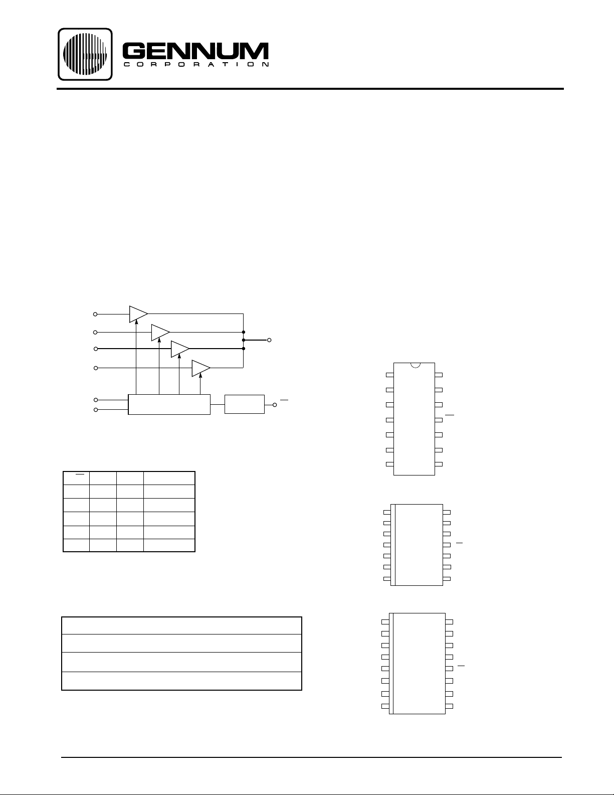
FUNCTIONAL BLOCK DIAGRAM
IN 0
IN 1
IN 2
IN 3
X
X
X
X
A0
A1
2 TO 4 DECODER
LOGIC
CHIP
SELECT
TRUTH TABLE
CS A1 A0 OUTPUT
0 0 0 IN 0
0 0 1 IN 1
0 1 0 IN 2
0 1 1 IN 3
1 X X HI - Z
X = DON'T CARE
ORDERING INFORMATION
= 75 Ω)
IN
OUTPUT
CS
CIRCUIT DESCRIPTION
The GX214A is a low cost 4x1 video multiplexer containing
four analog video switches and a 2 to 4 decoder. A Chip
Select input allows paralleled GX214As to be operated in
a switching matrix.
The GX214A represents a fully buffered, unilateral transmission
path when enabled. When disabled, the output is high
impedance.
The device operates from ±7.5 V to ±9.5 V supplies with
TTL and 5 V CMOS compatible input logic levels.
APPLICATIONS
• CATV and CCTV systems
• low cost video routing
Pin 1
14 PIN DIP
Pin 1
7
14 PIN SOIC
14
8
14
VCC
AO
A1
CS
OUT
LOGIC GND
V
8
EE
VCC
AO
A1
CS
OUT
LOGIC GND
V
EE
SIG GND
SIG GND
SIG GND
IN 0
SIG GND
IN 1
SIG GND
IN 2
SIG GND
IN 3
IN 0
IN 1
IN 2
IN 3
7
PIN CONNECTION
PIN CONNECTION
Part Number Package Type Temperature Range
GX214 - ACDB 14 Pin DIP 0° to 70°C
GX214 - ACKC 16 Pin SOIC 0° to 70°C
GX214 - ACKB 14 Pin SOIC 0° to 70°C
IN 0
SIG GND
IN 1
SIG GND
IN 2
SIG GND
IN 3
NC
Pin 1
8 9
PIN CONNECTION
16 PIN SOIC
16
V
CC
NC
AO
A1
CS
OUT
LOGIC GND
V
EE
Document No. 520 - 5 - 1
GENNUM CORPORATION P.O. Box 489, Stn A, Burlington, Ontario, Canada L7R 3Y3 tel. (905) 632-2996 fax: (905) 632-5946
Japan Branch: A-302 Miyamae Village, 2-10-42 Miyamae, Suginami-ku, Tokyo 168, Japan tel. (03) 3334-7700 fax: (03) 3247-8839
ABSOLUTE MAXIMUM RATINGS
Parameter Value
Supply Voltage ±10.0 V
Operating Temperature Range 0 °C ≤ TA ≤ 70 °C
Storage Temperature Range -65 °C ≤ TS ≤ 150 °C
Parameter Value
Lead Temperature (Soldering, 10 Sec) 260 °C
Analog Input Voltage -4 V ≤ VIN ≤ VCC+0.3 V
Logic Input Voltage 0 V ≤ VL ≤ 5.5 V
NOTE: A short from output to ground or either supply will destroy the device.
For R
ELECTRICAL CHARACTERISTICS
use a 2.67 kΩ 1%, 1/4 W resistor.
EXT
VS = ±8 V DC, 0°C < TA < 70 °C, RL = 2.67 kΩ to VEE, CL = 30pF IL = 3mA
PARAMETER SYMBOL CONDITIONS MIN TYP MAX UNITS
Supply Voltage ± V
S
7.5 8.0 9.5 V
DC I+ Chip selected (CS=0) - 14 20 mA
SUPPLY Chip not selected (CS=1) - 0.5 0.85 mA
Supply Current
not including
I
L
Analog Output V
I- Chip selected (CS=0) - 13 18 mA
Chip not selected (CS=1) - 0.58 0.88 mA
OUT
Extremes before +5.0 V
Voltage Swing clipping occurs - - -1.2
STATIC Analog Input Bias I
IN
-25-µA
Current
Output Offset Voltage V
OS
75Ω resistor on each +5 -30 -70 mV
input to ground
Turn-On Time t
ON
Control input to appearance - 250 400 ns
of signal at output.
Turn-Off Time t
OFF
Control input to disappear- 500 750 - ns
ance of signal at output.
LOGIC Logic Input V
Thresholds V
Logic Input I
IH
IL
BIAS
1 2.4 - - V
0 - - 0.6 V
Chip Selected A0,A1 = 1 - - 1 nA
Bias Current Chip Selected A0,A1 = 0 - - 2 µ A
Insertion Loss I.L. 1V p-p sine or sq. wave 0.05 0.08 0.11 dB
at 100 kHz
Bandwidth (-3dB) B.W. 65 85 - MHz
Input Resistance R
DYNAMIC Input Capacitance C
IN
IN
Chip selected (CS = 0) 900 - - kΩ
Chip selected (CS = 0) - 2.0 - pF
Chip not selected (CS=1) - 2.2 - pF
Output Resistance R
Output Capacitance C
OUT
OUT
Chip selected (CS=0) - 14 - Ω
Chip not selected (CS=1) - 12 - pF
Differential Gain dg at 3.58 MHz - - 0.05 %
Differential Phase dp VIN = 40 IRE - - 0.05 deg.
Sweep on 3 inputs 1V p-p
All Hostile Crosstalk X
Chip Disabled Crosstalk X
520 - 5 - 1 2
TALK(AH)
TALK(CD)
4th input has 75 Ω resistor 72 75 - dB
to gnd. ƒ = 10 MHz
One xpt on output to ground 90 100 - dB
ƒ = 10 MHz

APPLICATION INFORMATION
The circuit layout of any wideband circuit is critical. Good
high frequency design practice, proper lead dress and
PCB component placement along with a well regulated and
decoupled power supply will assure optimum performance
of the crosspoint.
The GX214A is non-inverting. The inputs are buffered and
require 75Ω line terminating resistors when driven from 75Ω
cable. The inputs may be driven directly from an amplifier
which has low output impedance.
The output of the GX214A must be buffered to drive 7 Ω
lines. The addition of an amplifier/buffer also allows adjustments
to be made to the gain, offset and frequency response of
the circuit.
Signal Ground (SG) pins 2, 4 and 6 must be joined together
and preferably form part of a ground plane. The Signal
Ground must also be connected to the ± 8V power supply
ground. The potential of the Logic Ground (LG) pin 9 can
deviate from the Signal Ground by ±0.5V maximum. Alternatively,
the signal and logic grounds can be joined together at one
point only.
An external load current of 2 to 8mA should be supplied
from each output bus to negative supply. For most applications
a load resistor of 2.67kΩ, 1% is recommended to minimize
offset drift with temperature. In order to improve differential
phase and tighten the insertion loss tolerance, an external
constant current active load may be substituted for the
load resistor. Note however, that since only one GX214A
output drives the output bus at any one time, only one
external load is needed for the bus.
A typical application is shown below. Two GX214A ICs are
paralleled to form an 8x1 crosspoint matrix. The three
address lines make use of the A0, A1 and CS inputs. If more
than two devices are used in parallel, a decoder is necessary
in order to generate the extra address inputs.
Depending on the application and the speed of the logic
family used, latches may be required for synchronization
where timing delays are critical. The active switching
circuitry of the GX214A ensures low crosstalk and high performance over an input voltage range of -1.2 to +5.0 volts.
INPUTS VIDEO SWITCHES
0.1
1
V 0
V 1
V 2
V 3
V 4
V 5
V 6
V 7
IN 0
2
SG
3
IN 1
4
SG
5
IN 2
6
SG
7
IN 3
75
75 75
75 75
75
75
1
IN 0
2
SG
3
IN 1
4
SG
5
IN 2
6
SG
7
IN 3
75
+V
A 0
A 1
CS
OUT
LG
-V
0.1
0.1
+V
A 0
A 1
CS
OUT
LG
-V
0.1
+8V
14
13
12
11
10
9
8
-8V
+8V
14
13
12
11
10
9
8
-8V
2.67 K
All resistors in ohms, all capacitors
in microfarads, unless otherwise stated
GAIN, OFFSET, FREQUENCY
RESPONSE ADJUSTMENTS
75
AMPLIFIER/BUFFER
A 0
A 1
A 2
ADDRESS
V
OUT
Fig. 1 8x1 Video Multiplexer Incorporating Two GX214A Devices
520 - 5 - 13

TYPICAL PERFORMANCE CURVES FOR GX214A
= ±8V, C
V
S
5
4
3
2
1
0
GAIN (dB)
-1
-2
-3
-4
-5
1 10 100
FREQUENCY (MHz)
Fig. 2 Gain vs Frequency
= 30pF, IL = 3mA unless otherwise shown
L
0.0
-0.5
-1.0
-1.5
-2.0
-2.5
-3.0
PHASE (deg)
-3.5
-4.0
-4.5
-5.0
1 3 5 10
Fig. 3 Phase vs Frequency
FREQUENCY (MHz)
-20
-30
-40
-50
-60
-70
-80
GAIN (dB)
IN 1,2
-90
-100
-110
-120
1 10 100
XTALK (AH)
R
S
IN 0,3
=75Ω
OFF ISOLATION
=15Ω
R
L
FREQUENCY (MHz)
Fig. 4 All - Hostile Crosstalk & Off-Isolation vs Frequency
75
1
IN0
2
AG
FROM
NETWORK
ANALYSER
VCC V
+8V
14
*
* The power supply pins should be suitably decoupled with at least 0.1µF, high quality capacitors
All resistors in ohms, all capacitors in microfarads unless otherwise stated.
A0
A1
CS
OUT
LG
EE
8
0.05
0.04
V
=40 IRE
IN
0.03
0.02
)
o
0.01
0.00
-0.01
dg(%) dp(
-0.02
-0.03
-0.04
-0.05
1 3 5 10
dg
dp
FREQUENCY (MHz)
Fig. 5 Differential Gain & Phasevs Frequency
+5V
13
12
11
10
9
4
CLC110
2.67k
-8V
0.1
1
8
TO
5
NETWORK
ANALYSER
0.1
-5V
*
Fig. 6 Test Circuit
The TEST SET UP shown is for INPUT 0 tests. Similar circuitry is used for each input INPUT in order to test
FREQUENCY RESPONSE and PHASE DELAY. For OFF-ISOLATION, all switches are disabled (CHIP SELECT
= logic 1) and a second enabled GX214A is connected to the output bus. For ALL-HOSTILE CROSSTALK,
three OFF switches are driven from the generator and the fourth is terminated with a 75Ω resistor. For the
DIFFERENTIAL GAIN and PHASE tests, the output is AC coupled to the output amplifier and the input level
from the generator is modulated with a step signal varying between 0 volts DC and 0.714 volts DC.
520 - 5 - 1 4

REVISION NOTES
Block diagram added,new test circuit, revised electrical
characteristics, new application circuit, all new response graphs.
.
CAUTION
ELECTROSTATIC
SENSITIVE DEVICES
DO NOT OPEN PACKAGES OR HANDLE
EXCEPT AT A STATIC-FREE WORKSTATION
DOCUMENT
IDENTIFICATION
PRODUCT PROPOSAL
This data has been compiled for market investigation purposes
only, and does not constitute an offer for sale.
ADVANCE INFORMATION NOTE
This product is in development phase and specifications are
subject to change without notice. Gennum reserves the right to
remove the product at any time. Listing the product does not
constitute an offer for sale.
PRELIMINARY DATA SHEET
The product is in a preproduction phase and specifications are
subject to change without notice.
DATA SHEET
The product is in production. Gennum reserves the right to make
changes at any time to improve reliability, function or design, in
order to provide the best product possible.
Gennum Corporation assumes no responsibility for the use of any circuits described herein and makes no representations that they are free from patent infringement.
© Copyright July 1990 Gennum Corporation. Revision Date: February 1993. All rights reserved. Printed in Canada.
520 - 5 - 15
 Loading...