

Page 1
© 2000 Fairchild Semiconductor Corporation DS500051 www.fairchildsemi.com
September 1997
Revised April 2000
GTLP8T306 8-Bit LVTTL/GTLP Bus Transceiver
GTLP8T306
8-Bit LVTTL/GTLP Bus Transceiver
General Description
The GTLP8T306 is an 8-b it bus transceiver that p rovides
LVTTL to GTLP signal level translation. T he device provides a high speed i nterface between cards opera ting at
LVTTL logic levels and a backplane operating at GTLP
logic levels. High speed backplane operation is a direct
result of GTLP’s reduced output swing (<1V), reduced input
threshold levels and output edge rate control. The ed ge
rate control minimizes bus settling time. GTLP is a Fairchild
Semiconductor derivati ve of the Gunning Transceiver logic
(GTL) JEDEC standard JESD8-3.
Fairchild’s GTLP has in ternal ou tput e dge-rate control a nd
is process, voltage, and temperatur e (PVT) com pensated.
Its function is similar to BTL and GTL but with different output levels and receiver th reshold s. The GTLP ou tput LOW
level is typically less than 0 .5V, the output HIGH level is
1.5V and the receiver threshold is 1.0V.
Features
■ Bidirectional interface between GTL/GTLP and LVTTL
logic levels
■ Output Edge Rate Control to minimize noise on the
GTLP port
■ Power up/down/off high impedance for live insertion
■ Standard 245 function
■ CMOS technology for low power dissipation
■ 5V tolerant inputs and outputs on the A-Port
■ Bus-hold data inputs on the A-Port eliminates the need
for external pull-up resistors on unused inputs
■ LVTTL compatible driver and control inputs
■ Flow through pinout optimizes PCB layout
■ Open drain on GTLP to support wired-or connection
■ A-Port source/sink −24 mA/+24 mA
■ B-Port sink 50 mA
■ Recommended Operating Temperature −40°C to +85°C
Ordering Code:
Devices also availab le in Tape and Reel. Specify by appending th e s uffix let t er “X” to the ordering code.
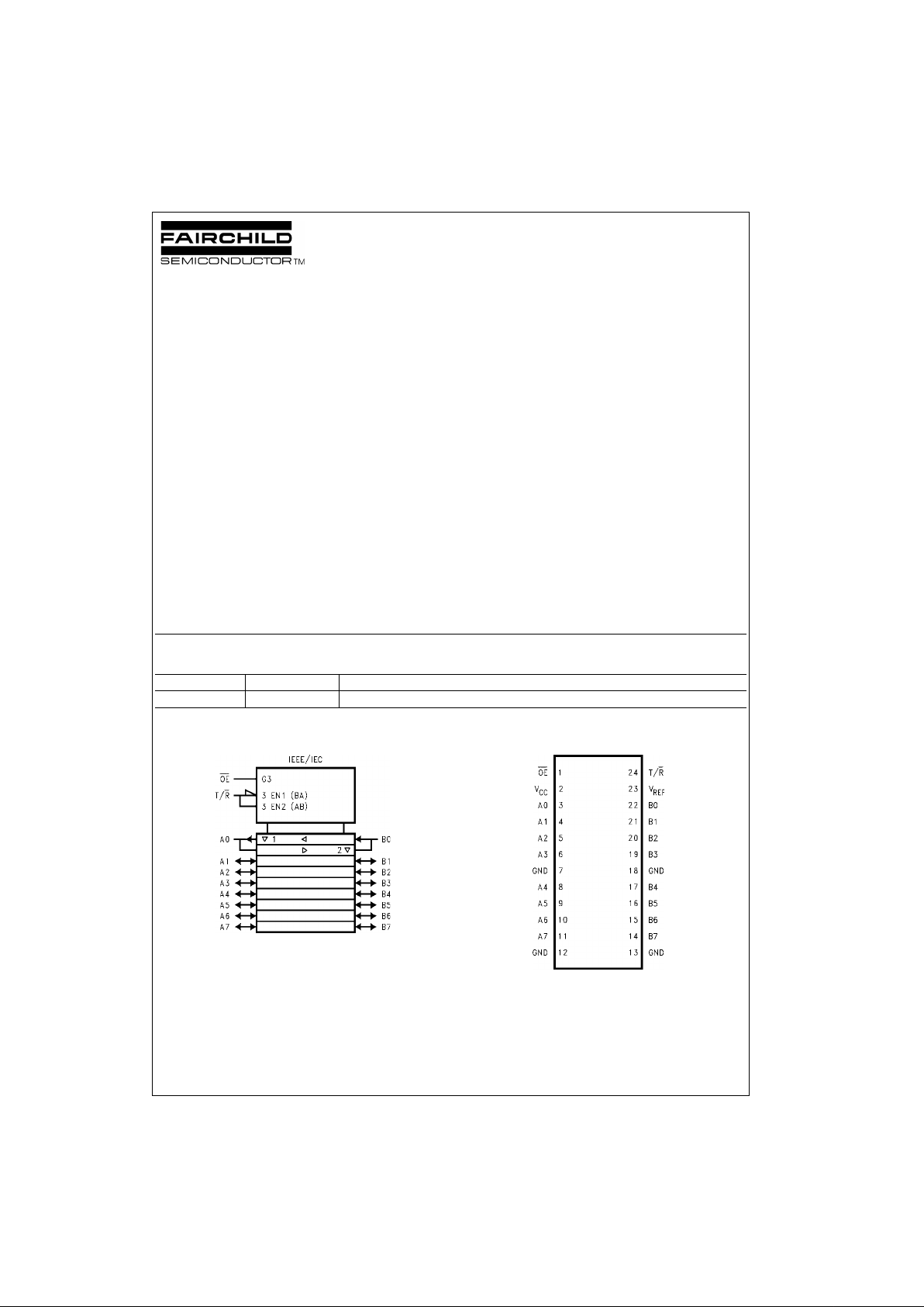
Logic Symbol Connection Diagram
Order Number Package Number Package Description
GTLP8T306MTC MTC24 24-Lead Thin Shrink Small Outline Package (TSSOP), JEDEC MO-153, 4.4mm Wide
Page 2
www.fairchildsemi.com 2
GTLP8T306
Pin Descriptions Tr uth Table
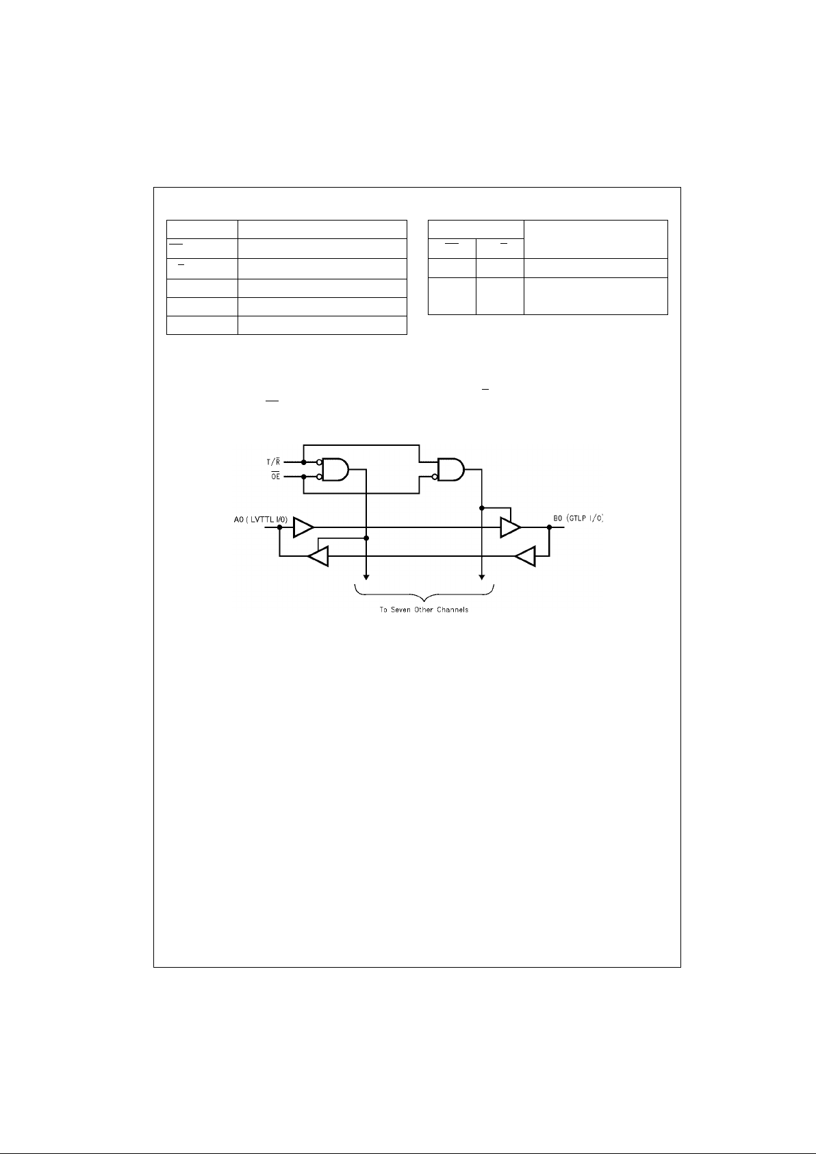
Functional Description
The GTLP8T306 i s an 8-b it transcei ver pro viding t he standa rd 245 f unctiona lity that supports bo th GTL a nd GTLP signal
levels.
Data polarity is non-inverting and the data flow direction is controlled by the T/R
pin. The outputs are enabled to allow data
through the device when OE
is LOW otherwise both the A and B ports are placed in a HIGH impedance state.
Logic Diagram
Pin Names Description
OE
Output Enable (Active LOW)
T/R
Transmit/Receive Input
A0–A7 Side A Inputs or 3-STATE Outputs
B0–B7 Side B Inputs or 3-STATE Outputs
V
REF
GTLP Reference Voltage
Inputs
Output
OE
T/R
H X HIGH Z on Bus A and Bus B
L L Bus B Data to Bus A
L H Bus A Data to Bus B
Page 3

3 www.fairchildsemi.com
GTLP8T306
Absolute Maximum Ratings(Note 1) Recommended Operating
Conditions
(Note 3)
Note 1: The Absolute Maxi mum Ratings are those v alues beyond which
the safety of the dev ice cannot b e guaranteed . The device sh ould not be
operated at these limit s. The parametric values defi ned in the Electrical
Characteristics tables are not guaranteed at the absolute maximum rating.
The “Recomm ended O peratin g Cond itions ” table will defin e the condition s
for actual device operation.
Note 2: I
O
Absolute Maximum Rating must be observed.
Note 3: Unused inputs must be held high or low.
Supply Voltage (VCC) −0.5V to 7.0V
DC Input Voltage (V
I
) −0.5V to +7.0V
DC Output Voltage (V
O
)
Outputs 3-STATE −0.5V to +7.0V
Outputs Active (Note 2) −0.5V to 7.0V
DC Output Sink Current into A-Port
I
OL
48 mA
DC Output Source Current from
A-Port I
OH
−48 mA
DC Output Sink Current into B-Port
in the LOW State, I
OL
100 mA
DC Input Diode Current (I
IK
)
V
I
< 0V −50 mA
DC Output Diode Current (I
OK
)
V
O
< 0V −50 mA
V
O
> V
CC
+50 mA
ESD Rating >2000V
Storage Temperature (T
STG
) −65°C to +150°C
Supply Voltage V
CC
3.15V to 3.45V
Bus Termination Voltage (V
TT
)
GTLP 1.35V to 1.65V
GTL 1.14V to 1.26V
Input Voltage (V
I
) on A-Port
and control pins 0V to 5.5V
HIGH Level Output Current (I
OH
)
A-Port −24 mA
LOW Level Output Current (I
OL
)
A-Port +24 mA
B-Port +50 mA
Operating Temperatur e (T
A
) −40°C to +85°C
Page 4

www.fairchildsemi.com 4
GTLP8T306
DC Electrical Characteristics
Over Recommended Operating Free-Air Temperature Range, V
REF
= 1.0V (unless otherwise noted).
Note 4: All typical values are VCC = 3.3V and TA= 25°C.
Note 5: For conditions shown as M in, us e the appropriate value s pecified under recommended operating con ditions.
Note 6: This is the increase in supply current for each input that is at the specified LVTTL voltage lev el rather than V
CC
or GND.
Symbol Test Conditions Min
Typ
(Note 4)
Max Units
V
IH
B-Port V
REF
+0.05 V
TT
V
Others 2.0 V
V
IL
B-Port 0.0 V
REF
−0.05 V
Others 0.8 V
V
REF
GTLP 1.0 V
GTL 0.8 V
V
IK
VCC = 3.15V II = −18 mA −1.2 V
V
OH
A-Port VCC = Min to Max
(Note 5)
IOH = −100 µAV
CC
−0.2
V
V
CC
= 3.15V IOH = −12 mA 2.4
I
OH
= −24 mA 2.0
V
OL
A-Port VCC = Min to Max
(Note 5)
IOL = 100 µA0.2
V
V
CC
= 3.15V IOL = 24 mA 0.5
B-Port VCC = 3.15V IOL = 40 mA 0.4
V
IOL = 50 mA 0.55
I
I
A-Port VCC = 3.45V VI = 5.5V 20
µA
V
I
= 0V −20
Control Pins V
CC
= 3.45V VI = 5.5V 5 µA
VI = 0V −5
B-Port VCC = 3.45V VI = V
TT
5
µA
VI = 0 −5
I
OFF
A-Port VCC = 0V
I
or VO= 0to4.5V 100 µA
II (Hold) A-Port VCC = 3.15V VI = 0.8V 75
µA
VI = 2.0V −20
I
OZH
A-Port VCC = 3.45V VO = 3.45V 20
µA
B-Port V
O
= 1.5V 5
I
OZL
A-Port VCC = 3.45V VO = 0 −20
µA
B-Port VCC = 3.45V VO = 0.55 −5
I
CC
A or B Ports VCC = 3.45V Outputs HIGH 7 18
mA
Outputs LOW 8 20
I
O
= 0
V
I
= VCC or GND Outputs Disabled 8 20
I
CC
A-Port and VCC = 3.45V One Input at VCC–0.6V 0 1
mA
(Note 6) Control Pins A or Control Inputs at
V
CC
or GND
C
IN
Control Pins VI = VCC or 0 5
pFA-Port VI = VCC or 0 7
B-Port VI = VCC or 0 9
Page 5

5 www.fairchildsemi.com
GTLP8T306
AC Electrical Characteristics
Over recommended range of supply voltage and operating free air-temperature, V
REF
= 1.0V (unless otherwise noted).
CL = 30 pF for B-Port and CL = 50 pF for A-Port.
Note 7: All typical values are at VCC = 3.3V and TA = 25°C.
Symbol From (Input) To (Output) Min
Typ
(Note 7)
Max Units
t
PLH
An Bn 1.0 4.0 7.5
ns
t
PHL
1.0 5.1 7.5
t
PLH
Bn An 1.0 5.8 8.3
ns
t
PHL
1.0 4.9 8.3
t
RISE
Transition Time, B Outputs (20% to 80%) 2.6 ns
t
FALL
Transition Time, B Outputs (20% to 80%) 2.6 ns
t
RISE
Transition Time, A Outputs (10% to 90%) 2.5 ns
t
FALL
Transition Time, A Outputs (10% to 90%) 2.5 ns
t
PZH
, t
PZL
OE An 1.0 4.5 9.5
ns
t
PHZ
, t
PLZ
1.0 4.9 9.5
t
PLH
OE Bn 1.0 5.4 9.5
ns
t
PHL
1.0 6.0 9.5
Page 6

www.fairchildsemi.com 6
GTLP8T306
Test Circuit and Timing Waveforms
Test Circuit for A Outputs
Voltage Waveforms Pulse Duration
(V
M
= VCC/2 for A-Port and 1.0 for B-Port)
Test Circuit for B Outputs
Voltage Waveforms Enable and Disable Times
A-Port
Voltage Waveforms Propagation Delay and Setup and Hold Times
(V
M
= VCC/2 for A-Port and 1.0 fo r B-Port)
Note A: CL includes probes and Jig capacitance.
Note B: For B-Port, C
L
= 30 pF is used for worst case.
Page 7

7 www.fairchildsemi.com
GTLP8T306 8-Bit LVTTL/GTLP Bus Transceiver
Physical Dimensions inches (millimeters) unless otherwise noted
24-Lead Thin S hrink Small Ou tline Package, JEDEC MO-153, 4.4mm Wide
Package Number MTC24
Fairchild does not assume any responsibility for use of any circuitry described , no circuit patent licenses are implied and
Fairchild reserves the right at any time without notice to change said circuitry and specifications.
LIFE SUPPORT POLICY
FAIRCHILD’S PRODUCTS ARE NOT AUTHORIZED FOR USE AS CRITICAL COMPONENTS IN LIFE SUPPORT
DEVICES OR SYSTEMS WITHOUT THE EXPRESS WRITTEN APPROVAL OF THE PRESIDENT OF FAIRCHILD
SEMICONDUCTOR CORPORATION. As used herein:
1. Life support devices or systems are dev ic es or syste ms
which, (a) are intended for surgical implant into the
body, or (b) support or sustain life, and (c) whose failure
to perform when properly used in accordance with
instructions for use provide d in the labe l ing, can be re asonably expected to result in a significant injury to the
user.
2. A critical compo nent in any com ponen t of a life s upp ort
device or system whose failure to perform can be reasonably expected to cause the failure of the l ife support
device or system, or to affect its safety or effectiveness.
www.fairchildsemi.com
 Loading...