

Page 1
© 1999 Fairchild Semiconductor Corporation DS500246 www.fairchildsemi.com
June 1999
Revised August 1999
GTLP6C817 Low Drive GTLP-to-LVTTL 1:6 Clock Driver
GTLP6C817
Low Drive GTLP-to-LVTTL 1:6 Clock Driver
General Description
The GTLP6C817 is a l ow drive clock driver tha t provides
TTL to GTLP signal lev el trans lation (and vice ver sa). The
device provides a high speed interface between cards
operating at TTL l ogic le vels and a backp lane o perat ing at
GTLP logic levels. H igh speed backplane operation is a
direct result of GTLP’s reduced output swing (<1V),
reduced input threshold leve ls and output edge rate control. The edge rate control minimizes bus settling time.
GTLP is a Fairchild Semiconduct or derivative of the Gunning Transceiver logic (GTL) JEDEC standard JESD8-3.
Fairchild’s GTLP has intern al edge -rate cont rol and is process, voltage, and temperature (PVT) compensated. Its
function is similar to BTL and GT L but with different outp ut
levels and receiver threshold. GTLP output LOW level is
typically less than 0. 5V, the output level HIGH is 1.5V and
the receiver threshold is 1.0V.
Features
■ Interface between TTL and GTLP logic levels
■ Edge Rate Control to minimize noise on the GTLP port
■ Power up/down high impedance for live insertion
■ 1:6 fanout clock driver for LVTTL port
■ 1:2 fanout clock driver for GTLP port
■ LVTTL compatible driver and control inputs
■ 5V over voltage tolerance on LVTTL ports
■ Flow through pinout optimizes PCB layout
■ Open drain on GTLP to support wired-or connection
■ Recommended Operating Temperature −40°C to +85°C
Ordering Code:
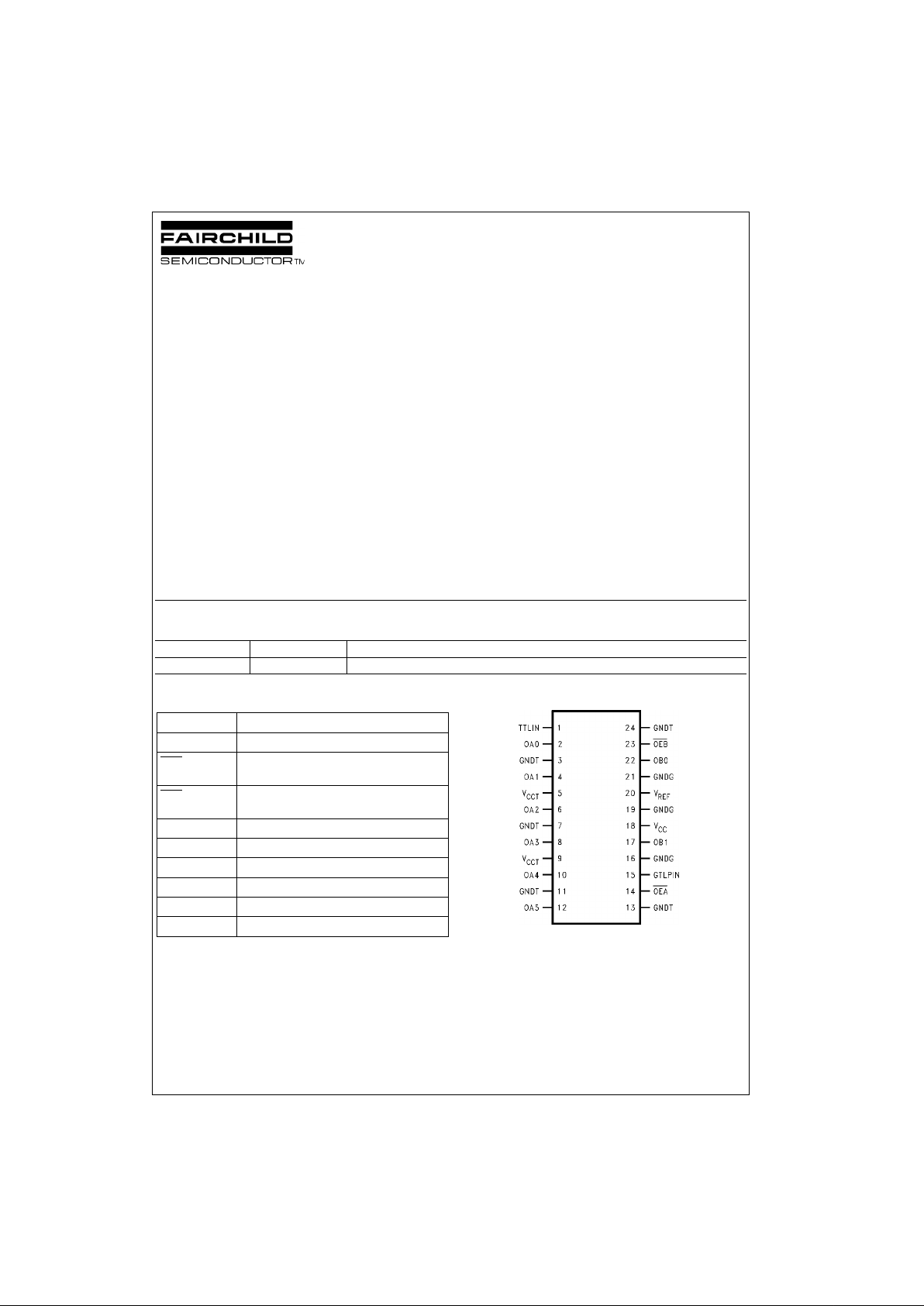
Pin Descriptions Connection Diagram
Order Number Package Number Package Description
GTLP6C817M TC MTC24 24-Lead Thin Shrink S m all Ou t li n e Pac ka ge ( TSSOP), JEDE C MO - 15 3 , 4. 4 mm W id e
Pin Names Description
TTLIN, GTLPIN Clock Inputs (TTL and GTLP respectively)
OEB
Output Enable (Active LOW)
GTLP Port (TTL Levels)
OEA
Output Enable (Active LOW)
TTL Port (TTL Levels)
V
CCT
.GNDT LVTTL Output Supplies (3V)
V
CC
Internal Circuitry VCC (5V)
GNDG OBn GTLP Output Grounds
V
REF
Voltage Reference Input
OA0–OA5 TTL Buffered Clock Outputs
OB0–OB1 GTLP Buffered Clock Outputs
Page 2
www.fairchildsemi.com 2
GTLP6C817
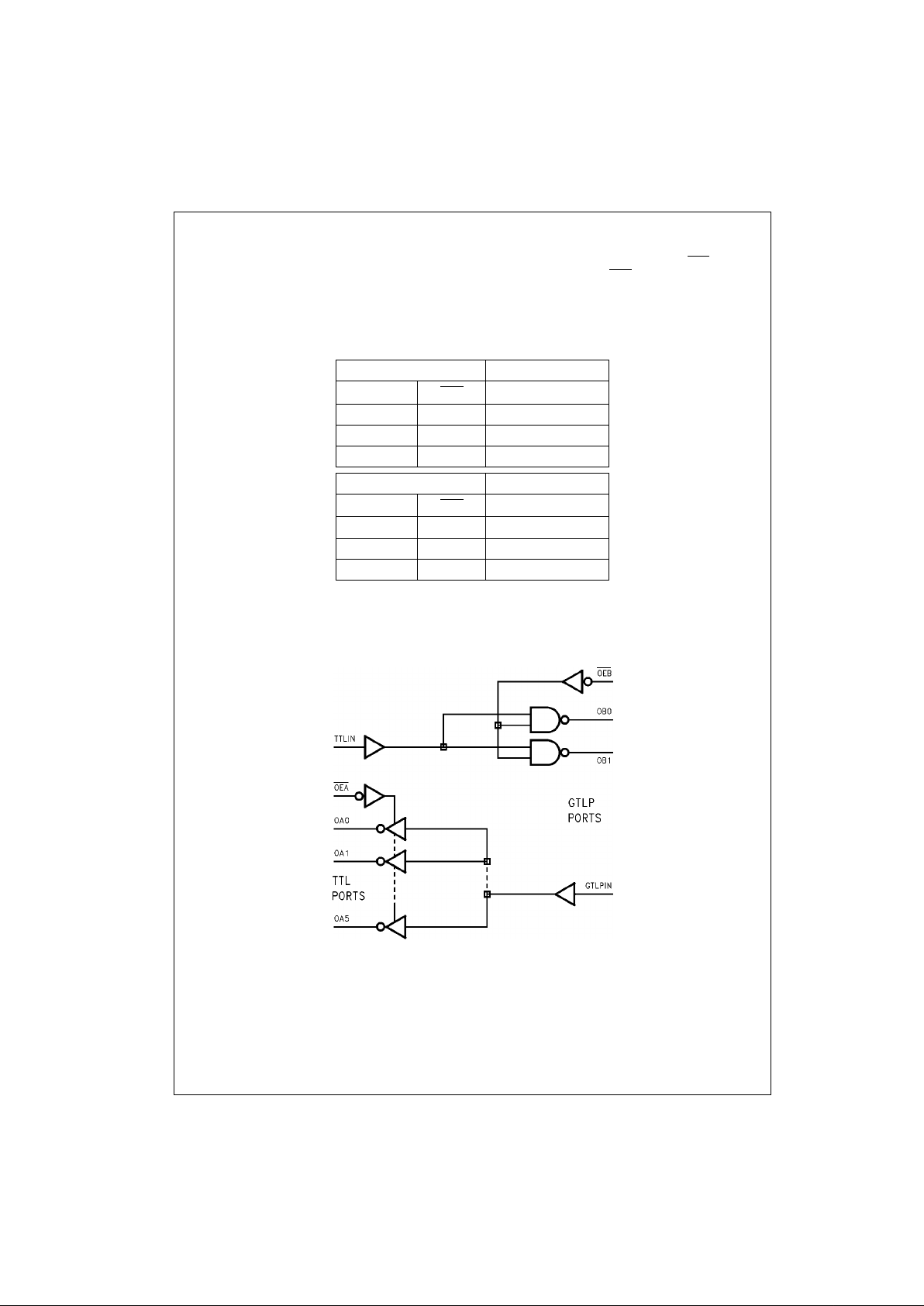
Functional Description
The GTLP6C817 is a low drive clock driver providing LVTTL-to-GTLP clock translation, and GTLP-to-LVTTL clock translation in the same packa ge. T he LVTTL-to-GTLP dire ction i s a 1:2 c lock dri ver pa th wit h a single Enab le pin (O EB
). For the
GTLP-to-LVTTL direction the clock receiver path is a 1:6 buffer with a single Enable control (OEA
). Data polarity is inverting
for both directions.
Truth Tables
Logic Diagram
Inputs Outputs
TTLIN OEB
OBn
HL L
LL H
X H High Z
Inputs Outputs
GTLPIN OEA
OAn
HL L
LL H
X H High Z
Page 3

3 www.fairchildsemi.com
GTLP6C817
Absolute Maximum Ratings(Note 1) Recommended Operating
Conditions
(Note 3)
Note 1: Absolute Maximum continuous ratings are those values beyond
which damage t o the device ma y occur. Exposure to t hese condition s or
conditions beyon d those indicated m ay adversely affect dev ice reliability.
Functional operation under absolute maximum rated conditions is not
implied.
Note 2: I
o
Absolute Maximum Rating must be observed.
Note 3: Unused input must be held HIGH or LOW.
Supply Voltage (VCC) −0.5V to +7.0V
DC Input Voltage (V
I
) −0.5V to +7.0V
DC Output Voltage (V
O
)
Outputs 3-STATE −0.5V to +7.0V
Outputs Active (Note 2) −0.5V to +7.0V
DC Output Sink Current into
OA-Port I
OL
24 mA
DC Output Source Current
from OA-Port I
OH
−24 mA
DC Output Sink Current into
OB-Port in the LOW State I
OL
80 mA
DC Input Diode Current (I
IK
)
V
I
< 0V −50 mA
DC Output Diode Current (I
OK
)
V
O
< 0V −50 mA
V
O
> V
CC
+50 mA
ESD Rating > 2000V
Storage Temperature (T
STG
) −65°C to +150°C
Supply Voltage
V
CC
4.75V to 5.25V
V
CCT
3.15V to 3.45V
Bus Termination Voltage (V
TT
)
GTLP 1.47V to 1.53V
V
REF
0.98V to 1.02V
Input Voltage (V
I
) on INA-Port
and Control Pins 0.0V to 5.5V
HIGH Level Output Current (I
OH
)
OA-Port −12 mA
LOW Level Output Current (I
OL
)
OA-Port +12 mA
OB-Port +40 mA
Operating Temperature (T
A
) −40°C to +85°C
Page 4

www.fairchildsemi.com 4
GTLP6C817
DC Electrical Characteristics
Over Recommended Operating Free-Air Temperature Range, V
REF
= 1.0V (unless otherwise noted).
Note 4: All typical va lues are at VCC = 5.0V V
CCT
= 3.3V and TA = 25°C.
Note 5: GTLP V
REF
and VTT are specified to 2% tolera nce sinc e sign al inte grity an d no ise ma rgin can be sign ificant ly de grade d if th ese sup pli es are noisy.
In addition, V
TT
and R
TERM
can be adjus t ed to accommo date backplane im pedances other t han 50Ω, within the boun da ries of no t exce edi ng the DC Abs o-
lute I
OL
ratings. Similarly V
REF
can be adjusted to com pensate for changes in VTT.
Symbol Test Conditions Min
Typ
Max Units
(Note 4)
V
IH
GTLPIN V
REF
+ 0.05 V
TT
V
Others 2.0
V
IL
GTLPIN 0.0 V
REF
− 0.05
V
Others 0.8
V
REF
GTLP 1.0
V
(Note 5) GTL 0.8
V
TT
GTLP 1.5
V
(Note 5) GTL 1.2
V
IK
VCC = 4.75V
II = −18 mA −1.2 V
V
CCT
= 3.15V
V
OH
OAn-Port VCC = 4.75V IOH = −100 µAV
CC
− 0.2
VV
CCT
= 3.15V IOH = −6 mA 2.4
IOH = −12 mA 2.2
V
OL
OAn-Port VCC = 4.75V IOL = 100 µA0.2
VV
CCT
= 3.15V IOL = 6 mA 0.4
IOL = 12 mA 0.5
V
OL
OBn-Port VCC = 4.75V IOL = 100 µA0.2
V
V
CCT
= 3.15V IOL = 40 mA 0.5
I
I
TTLIN/ VCC = 5.25V VI = 5.25V 5
µA
Control Pins V
CCT
= 3.45V VI = 0V −5
GTLPIN VCC = 5.25V VI = V
TT
5
µA
V
CCT
= 3.45V VI = 0 −5
I
OFF
TTLIN, OAn-Port, Control Pins VCC = 0V
I
or VO = 0V to 5.25V 30
µA
GTLPIN, OBn-Port V
CCT
= 0V
I
or VO = 0 to V
TT
30
I
OZH
OAn-Port VCC = 5.25V VO = 5.25V 5
µA
OBn-Port V
CCT
= 3.45V VO = 1.5V 5
I
OZL
OAn-Port VCC = 5.25V VO = 0
−5 µA
OBn-Port V
CCT
= 3.45V VO = 0
I
PU/PD
All Ports VCC = V
CCT
= 0 to 1.5V
OE = Don’t Care
30 µA
ICC (5V) OAn or VCC = 5.25V Outputs HIGH 10
mA
OBn Ports V
CCT
= 3.45V Outputs LOW 10
Outputs Disabled 10
VI = VCC or GND
ICC (3V) OAn or VCC = 5.25V Outputs HIGH, LOW 45
µAOBn Ports V
CCT
= 3.45V Outputs Disabled 45
VI = VCC or GND
∆I
CC
TTLIN VCC = 5.25V
VI = VCC−2.1 1 mA
V
CCT
= 3.45V
C
IN
Control Pins/GTLPIN/TTLIN VI = VCC or 0 3 3.5 pF
C
OUT
OAn-Port VI = VCC or 0 3 4.5
pF
OBn-Port VI = VCC or 0 4 5
Page 5

5 www.fairchildsemi.com
GTLP6C817
AC Electrical Characteristics
Over recommended range of supply voltage and operating free air temperature. V
REF
= 1.0V (unless otherwise noted).
CL = 30 pF for OBn-Port and CL = 50 pF for OAn-Port.
Note 6: All typical value s are at VCC = 5.0V and TA = 25°C.
Extended Electrical Characteristi cs
Over recommended ranges of supply voltage and operating free-air temperature V
REF
= 1.0V (unless otherwise noted).
CL = 30 pF for B Port and CL = 50 pF for A Port.
Note 7: All typical value s are at VCC = 5.0V and TA = 25°C.
Note 8: t
OSHL/tOSLH
and t
OST
- Output-to-Output skew is defined as the absolute value of the difference between the actual pro pagation delay for all outputs
within the same packaged device. T he specifications a re given for specif ic w orst case V
CC
and temperature and apply to any outputs switching in the same
direction either HIGH -to-LOW (t
OSHL
) or LOW-to-HIGH (t
OSLH
) or in opposite direct ions both HL and LH (t
OST
). This parameter is guaranteed by desi gn and
statistical process dis tributio n. Actua l skew v alues be tween t he GTLP outputs could vary on the backplan e due to t he loadin g and imp edanc e seen by t he
device.
Note 9: t
PS
- Pin or Transition skew is defined as the difference between the LOW-to-HIGH transition and the HIGH-to-LOW transition on the same pin. The
parameter is me as ured across all the outputs of the s ame chip is spec if ied for a specific w orst case V
CC
and temperature. This paramet er is guaranteed by
design and statistical pro cess distribu tion. Actu al skew values between the GTL P outputs coul d vary on the bac kplane due to the loading and imp edance
seen by the device.
Note 10: t
PV
- Part-to-Part skew is defined as the absolute va lue of the differe nce between the actual prop agation design for all outputs fro m device-to-
device. The para mete r is spec ifie d fo r a s pec ific w ors t cas e V
CC
and temperature. This par ameter is guarante ed by design and statistic al proce ss distribution. Actual skew valu es between the GTLP out put could vary on the backplane due to the loading and impedance se en by the device.
Note 11: Due to the open drain stru cture o n G TLP outp uts, t
OST
and t
PV(LH)
in the A-to-B direct ion are no t spec ified . Skew on t hese path s is de pen dent on
the V
TT
and RT values in the actual application.
Symbol From (Input) To (Output) Min
Typ
Max Units
(Note 6)
t
PLH
TTLIN OBn 2.3 4.7
ns
t
PHL
1.5 4.6
t
PLH
OEB OBn 2.4 4.8
ns
t
PHL
1.6 4.7
t
RISE
Transition Time, OB Outputs (20% to 80%) 1.7 ns
t
FALL
Transition Time, OB outputs (20% to 80%) 2.1 ns
t
RISE
Transition Time, OA outputs (10% to 90%) 2.7 ns
t
FALL
Transition Time, OA outputs (10% to 90%) 2.2 ns
t
PZH
, t
PZL
OEA OAn 2.4 6.5
ns
t
PLZ
, t
PHZ
2.0 6.5
t
PLH
GTLPIN OAn 3.1 6.6
ns
t
PHL
2.8 6.0
Symbol
From To
Min
Typ
Max Unit
(Input) (Output) (Note 7)
t
OSLH
(Note 8) A B .05 .4 ns
t
OSHL
(Note 8) A B .05 .4
t
PS
(Note 9) A B 0.5 1.0 ns
t
PV(HL)
(Note 10)
AB .7ns
(Note 11)
t
OSLH
(Note 8) B A .12 .5
ns
t
OSHL
(Note 8) B A .12 .5
t
OST
(Note 8) B A .6 1.0 ns
t
PS
(Note 9) B A 0.5 1.0 ns
t
PV
(Note 10) B A 1.2 ns
Page 6

www.fairchildsemi.com 6
GTLP6C817
Test Circuit and Timing Waveforms
Test Circuit for A Outputs
Note A: C
L
includes probes and jig capa citance.
Test Circuit for B Outputs
Note A: CL includes probes and jig capacitance.
Note B: For B Port C
L
= 30 pF is used for worst case.
Voltage Waveform - Propagation Delay Times Voltage Waveform - Enable and Disable Times
Output Waveform 1 is for an out put with intern al conditio ns such that the
output is LOW excep t when disabled by the control output
Output Waveforms 2 is for an out put wit h inte rnal condition s such that the
output is HIGH excep t wh en disabled by the cont rol output
Input and Measure Conditions
All input pulses have the following characteristics: Frequency = 10MHz, t
RISE
= t
FALL
= 2 ns, ZO = 50Ω.
The outputs are meas ured one at a time with on e t ransition per measurement.
A or LVTTL
Pins
B or GTLP
Pins
V
inHIGH
V
CC
1.5
V
inLOW
0.0 0.0
V
M
VCC/2 1.0
V
X
VOL + 0.3V N/A
V
Y
VOH + 0.3V N/A
Page 7

7 www.fairchildsemi.com
GTLP6C817 Low Drive GTLP-to-LVTTL 1:6 Clock Driver
Physical Dimensions inches (millimeters) unless otherwise noted
24-Lead Thin Shrink Small Outline Package (TSSOP), JEDEC MO-153, 4.4mm Wide
Package Number MTC24
Fairchild does not assume any responsibility for use of any circu itry described, no circuit patent license s are implied and
Fairchild reserves the right at any time without notice to change said circuitry and specifications.
LIFE SUPPORT POLICY
FAIRCHILD’S PRODUCTS ARE NOT AUTHORIZED FOR USE AS CRITICAL COMPONENTS IN LIFE SUPPORT
DEVICES OR SYSTEMS WITHOUT THE EXPRESS WRITTEN APPROVAL OF THE PRESIDENT OF FAIRCHILD
SEMICONDUCTOR CORPORATION. As used herein:
1. Life sup por t de vices o r syst ems are devices or systems
which, (a) are intended for surgical implant into the
body, or (b) support or sustain life, and (c) whose failure
to perform when properly used in accordance with
instructions for use provided i n the labe li ng, can be re asonably expected to result in a significant injury to the
user.
2. A criti cal com ponen t in any compo nent o f a li fe supp ort
device or system whose failu re to perform can b e reasonably expected to c ause th e fa i lure of the li fe s upp or t
device or system, or to affect its safety or effectiveness.
www.fairchildsemi.com
 Loading...