

Page 1
June 1998
Revised October 1998
GTLP6C816 GTLP-to-TTL 1:6 Clock Driver
© 1998 Fairchild Semiconductor Corporation DS500129.prf www.fairchildsemi.com
GTLP6C816
GTLP-to-TTL 1:6 Clock Driver
General Description
The GTLP6C816 is a clock driver that provides TTL to
GTLP signal level translation (and vice versa). The devi ce
provides a high speed interface between cards operating at
TTL logic levels and a backpl ane operating at GT LP logic
levels. High speed backplane operation is a direct result of
GTLP’s reduced output swi ng (<1 V), re duced input th reshold levels and output edge rate co ntr ol. Th e ed ge ra te co ntrol minimizes bus settling time. GTLP is a Fairchild
Semiconductor derivati ve of the Gunning Transceiver logic
(GTL) JEDEC standard JESD8-3.
Fairchild’s GTLP has intern al edge -rate cont rol and is process, voltage, and temperature (PVT) compensated. Its
function is similar to BTL and GT L but with different outp ut
levels and receiver threshold. GTLP output LOW level is
typically less than 0.5V, the output level HIGH is 1.5V and
the receiver threshold is 1.0V.
Features
■ Interface between TTL and GTLP logic levels
■ Edge Rate Control to minimize noise on the GTLP port
■ Power up/down high impedance for live insertion
■ 1:6 fanout clock driver for TTL port
■ 1:2 fanout clock driver for GTLP port
■ TTL compatible driver and control inputs
■ Flow through pinout op timizes PCB layout
■ Open drain on GTLP to support wired-or connection
■ Recommended Operating Temperature −40°C to +85°C
Ordering Code:
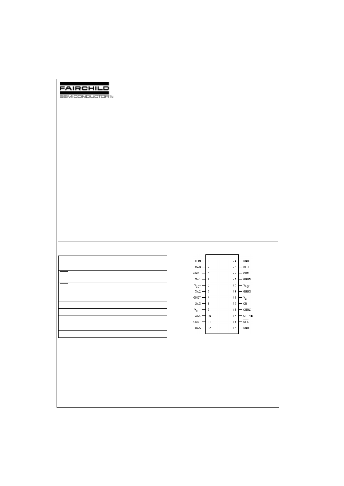
Pin Descriptions Connection Diagram
Order Number Package Number Package Description
GTLP6C816M TC MTC24 24-Lead Thin Shrink Sm al l Ou t li n e Pac k age ( TSSOP), JE DE C MO - 15 3 , 4. 4m m W i de
Pin Names Description
TTLIN, GTLPIN Clock Inputs (TTL and GTLP respectively)
OEB
Output Enable (Active LOW)
GTLP Port (TTL Levels)
OEA
Output Enable (Active LOW)
TTL Port (TTL Levels)
V
CCT
.GNDT TTL Output Supplies (5V)
V
CC
Internal Circuitry VCC (5V)
GNDG OBn GTLP Output Grounds
V
REF
Voltage Reference Input
OA0–OA5 TTL Buffered Clock Outputs
OB0–OB1 GTLP Buffered Clock Outputs
Page 2
www.fairchildsemi.com 2
GTLP6C816
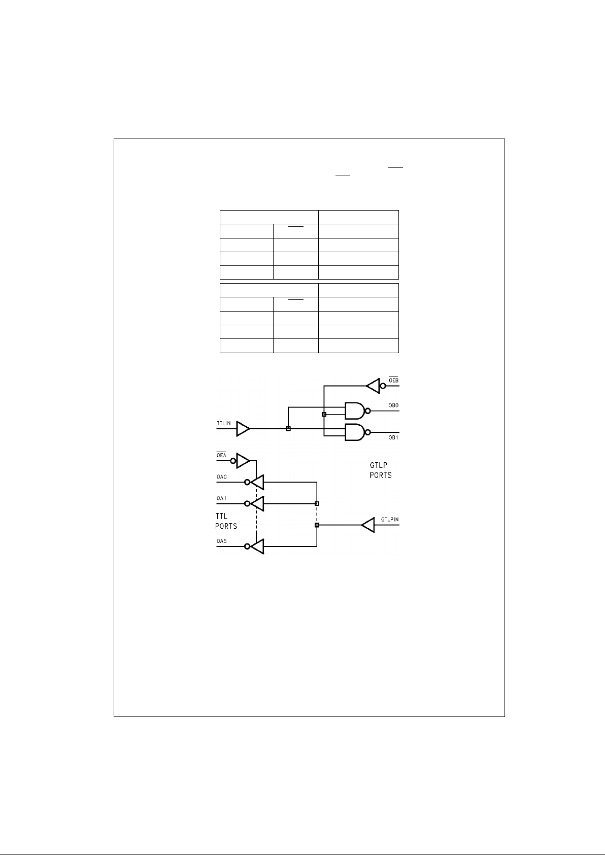
Functional Description
The GTLP6C816 is a clock driver providing TTL-to-GTLP clock translation, and GTLP-to-TTL clock translation in the same
package. The TTL-to- GT LP dir ecti o n is a 1 :2 cl oc k driv e r pa th wit h a si n gle E na ble p in (O E B
). For the GTLP-to-T T L dir ec-
tion the clock receiver path is a 1:6 buffer with a single Enable control (OEA
). Data polarity is inverting for both directions.
Truth Tables
Logic Diagram
Inputs Outputs
TTLIN OEB
OBn
HL L
LL H
X H High Z
Inputs Outputs
GTLPIN OEA
OAn
HL L
LL H
X H High Z
Page 3

3 www.fairchildsemi.com
GTLP6C816
Absolute Maximum Ratings(Note 1) Recommended Operating
Conditions
(Note 3)
Note 1: Absolute Maximum continuous ratings are those values beyond
which damage t o the device ma y occur. Exposure to t hese condition s or
conditions beyon d those indicated m ay adversely affect dev ice reliability.
Functional operation under absolute maximum rated conditions is not
implied.
Note 2: I
o
Absolute Maximum Rating must be observed.
Note 3: Unused input must be held h igh or low.
Supply Voltage (VCC) −0.5V to +7.0V
DC Input Voltage (V
I
) −0.5V to +7.0V
DC Output Voltage (V
O
)
Outputs 3-STATE −0.5V to +7.0V
Outputs Active (Note 2) −0.5V to +7.0V
DC Output Sink Current into
OA-Port I
OL
48 mA
DC Output Source Current
from OA-Port I
OH
−48 mA
DC Output Sink Current into
OB-Port in the LOW State I
OL
80 mA
DC Input Diode Current (I
IK
)
V
I
< 0V −50 mA
DC Output Diode Current (I
OK
)
V
O
< 0V −50 mA
V
O
> V
CC
+50 mA
ESD Rating > 2000V
Storage Temperature (T
STG
) −65°C to +150°C
Supply Voltage V
CC
4.75V to 5.25V
Bus Termination Voltage (V
TT
)
GTLP 1.47V to 1.53V
V
REF
0.98V to 1.02V
Input Voltage (V
I
) on INA-Port
and Control Pins 0.0V to 5.5V
HIGH Level Output Current (I
OH
)
OA-Port −24 mA
LOW Level Output Current (I
OL
)
OA-Port +24 mA
OB-Port +34 mA
Operating Temperature (T
A
) −40°C to +85°C
Page 4

www.fairchildsemi.com 4
GTLP6C816
DC Electrical Characteristics
Over Recommended Operating Free-Air Temperature Range, V
REF
= 1.0V (unless otherwise noted).
Note 4: All typical va lues are at VCC = 5.0V and TA = 25°C.
Note 5: GTLP V
REF
and VTT are specified to 2% tolera nce sinc e sign al inte grity an d no ise ma rgin can be sign ificant ly de grade d if th ese sup pli es are noisy.
In addition, V
TT
and R
TERM
can be adjus t ed to accommo date backplane im pedances other t han 50Ω, within the boun da ries of no t exce edi ng the DC Abs o-
lute I
OL
ratings. Similarly V
REF
can be adjusted to com pensate for changes in VTT.
Symbol Test Conditions Min
Typ
(Note 4)
Max Units
V
IH
GTLPIN V
REF
+0.05 V
TT
V
Others 2.0
V
IL
GTLPIN 0.0 V
REF
−0.05
V
Others 0.8
V
REF
GTLP 1.0
V
(Note 5) GTL 0.8
V
TT
GTLP 1.5
V
(Note 5) GTL 1.2
V
IK
VCC = 4.75V II = −18 mA −1.2 V
V
OH
OAn-Port VCC = 4.75V IOH = −100 µAV
CC
−0.2
VIOH = −18 mA 2.4
IOH = −24 mA 2.2
V
OL
OAn-Port VCC = 4.75V IOL = 100 µA0.2
VIOL = 18 mA 0.4
IOL = 24 mA 0.5
V
OL
OBn-Port VCC = 4.75V IOL = 100 µA0.2
V
IOL = 34 mA 0.65
I
I
TTLIN/ VCC = 5.25V VI = 5.25V 5
µA
Control Pi ns VI = 0V −5
GTLPIN VCC = 5.25V VI = V
TT
5
µA
VI = 0 −5
I
OFF
TTLIN VCC = 0V
I
or VO = 0V to
5.25V
100 µA
I
OZH
OAn-Port VCC = 5.25V VO = 5.25V 5
µA
OBn-Port VO = 1.5V 5
I
OZL
OAn-Port VCC = 5.25V VO = 0 −5 µA
I
CC
OAn or VCC = 5.25V Outputs HIGH 7 18
OBn Ports Outputs LOW 7 20 mA
VI = VCC or GND Outputs Disabled 7 20
∆I
CC
TTLIN VCC = 5.25V VI = VCC−2.1 6 mA
C
IN
Control Pi ns / GTLPIN/
TTLIN
VI = VCC or 0
3.7 pF
C
OUT
OAn-Port VI = VCC or 0 7
pF
OBn-Port VI = VCC or 0 7
Page 5

5 www.fairchildsemi.com
GTLP6C816
AC Electrical Characteristics
Over recommended range of supply voltage and operating free air temperature. V
REF
= 1.0V (unless otherwise noted).
CL = 30 pF for OBn-Port and CL = 50 pF for OAn-Port.
Note 6: All typical value s are at VCC = 5.0V and TA = 25°C.
Note 7: Skew specs are given for specific worst case V
CC
Temp. Skew values between t he OB n outp uts cou ld vary on t he bac kplane due t o loadin g and
impedance seen by the device.
Symbol From (Inpu t) To (Output) Min
Typ
(Note 6)
Max Units
t
PLH
TTLIN OBn 1.5 3.8 6.0
ns
t
PHL
1.5 2.8 5.0
t
PLH
OEB OBn 1.5 6.4 10.5
ns
t
PHL
1.5 3.2 6.0
t
RISE
Transition Time, OB Outputs (20% to 80%) 2.3 ns
t
FALL
Transition Time, OB outputs (20% to 80%) 2.3 ns
t
RISE
Transition Time, OA outputs (10% to 90%) 2.0 ns
t
FALL
Transition Time, OA outputs (10% to 90%) 2.0 ns
t
PZH
, t
PZL
OEA OAn 0.5 3.6 6.5
ns
t
PLZ
, t
PHZ
0.5 3.8 6.5
t
PLH
GTLPIN OAn 1.5 4.4 6.5
ns
t
PHL
1.5 4.0 6.0
t
OSHL
, t
OSLH
(Note 7)
Common Edge Skew 0.2 1.0
ns
Page 6

www.fairchildsemi.com 6
GTLP6C816
Test Circuit and Timing Waveforms
Test Circuit for A Outputs
Note A: C
L
includes probes and jig capacitance.
Test Circuit for B Outputs
Note A: C
L
includes probes and jig capacitance.
Note B: For B-Port C
L
= 30 pF is used for worst case.
Voltage Waveforms Enable and Disable Times A-Port
Voltage Waveforms Propagation Delay (V
m
= VCC/2 for A-Port and 1.0 for B-Port)
Page 7

Fairchild does not assume any responsibility for use of any circuitry described, no circuit patent licenses are implied and Fairchild reserves the right at any time without notice to change said circuitry and specifications.
GTLP6C816 GTLP-to-TTL 1:6 Clock Driver
LIFE SUPPORT POLICY
FAIRCHILD’S PRODUCTS ARE NOT AUTHORIZED FOR USE AS CRITICAL COMPONENTS IN LIFE SUPPORT
DEVICES OR SYSTEMS WITHOUT THE EXPRESS WRITTEN APPROVAL OF THE PRESIDENT OF FAIRCHILD
SEMICONDUCTOR CORPORATION. As used herein:
1. Life support devices or systems are devices or systems
which, (a) are intended for surgical implant into the
body, or (b) support or sustain life, and (c) whose failure
to perform when properly used in accordance with
instructions for use provide d in the lab el ing , can be re asonably expected to result in a significant in jury to the
user.
2. A critical component in any component of a life support
device or system whose failure to perform can be r easonably expected to cau se th e f ail ur e o f the life sup por t
device or system, or to affect its safety or effectiveness.
www.fairchildsemi.com
Physical Dimensions inches (millimeters) unless otherwise noted
24-Lead Thin Shrink Small Outline Package (TSSOP), JEDEC MO-153, 4.4mm Wide
Package Number MTC24
 Loading...