

Datasheet GTLP18T612MTDX, GTLP18T612MTD, GTLP18T612MEAX, GTLP18T612MEA Datasheet (Fairchild Semiconductor)
Page 1
© 1999 Fairchild Semiconductor Corporation DS500169 www.fairchildsemi.com
May 1999
Revised September 1999
GTLP18T612 18-Bit LVTTL/GTLP Universal Bus Transceiver
GTLP18T612
18-Bit LVTTL/GTLP Universal Bus Transceiver
General Description
The GTLP18T612 is an 18-bit universal bus transceiver
which provides LVTTL to GTLP sign al level translation. It
allows for transparent, latched and clocked modes of data
transfer. The device provides a high speed interface for
cards operating at LVTTL logic levels and a backplane
operating at GTLP logic levels. High speed backplane
operation is a direct res ult of GTL P ’s reduced out put sw ing
(< 1V), reduced input threshold levels and output edge rate
control. The edge rate c ontrol min imizes b us settli ng time.
GTLP is a Fairchild Semiconduct or derivative of the Gunning Transistor logic (GTL) JEDEC standard JESD8-3.
Fairchild's GTLP has inte rnal ed ge-ra te cont rol and is Process, Voltage, and Temperature (PVT) compensated. Its
function is similar to BTL or GTL but with different output
levels and receiver thresholds. GTLP outpu t LOW level is
less than 0.5V, the output HIGH is 1.5V and the receiver
threshold is 1.0V.
Features
■ Bidirectional interface between GTLP and LVTTL logic
levels
■ Edge Rate Control to minimize noise on the GTLP port
■ Power up/down high impedance for live insertion
■ External V
REF
pin for receiver threshold
■ BiCMOS technology for low power dissipation
■ Bushold data input s on A Port eliminates the need for
external pull-up resistors for unused inputs
■ LVTTL compatible Driver and Control inputs
■ Flow-through architecture optimizes PCB layout
■ Open drain on GTLP to support wired-or connection
■ A-Port source/sink −24 mA/+24 mA
■ B-Port sink capability +50 mA
■ D-type flip-flop, latch and transparent data paths
Ordering Code:
Device also available in Tape and Reel. Specify by appending s uffix let te r “X” to the ordering code.
Order Number Package Number Package Description
GTLP18T612MEA MS56A 56-Lead Shrink Small Outline Package (SSOP), JE DEC MO-118, 0.300” Wide
GTLP18T612MTD MTD56 56-Lead Thin Shrink Small Outline Package (TSSOP), JEDEC MO-153, 6.1mm Wide
Page 2
www.fairchildsemi.com 2
GTLP18T612
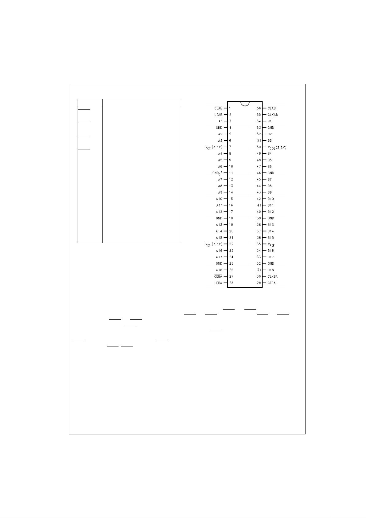
Pin Descriptions Connection Diagram
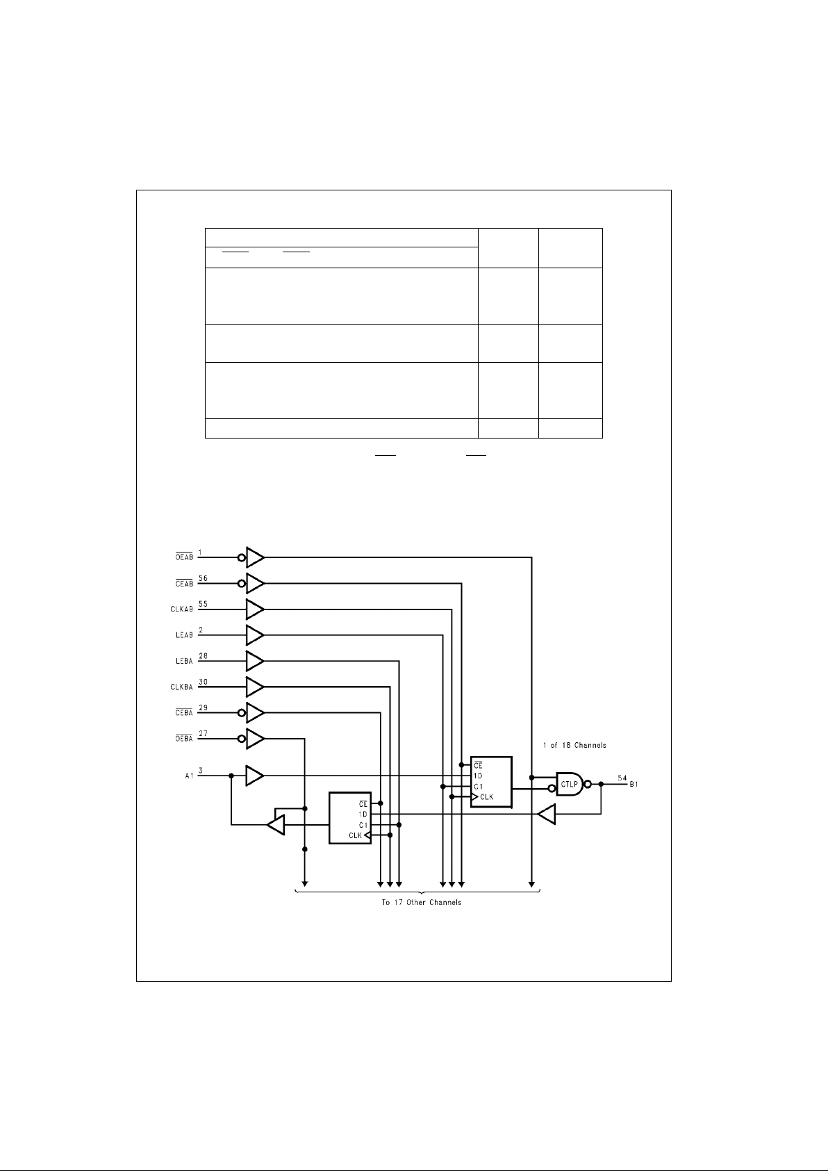
Functional Description
The GTLP18T612 is an 18 bit registered transceiver containing D-type flip-flop, latch and transparent modes of operation
for the data path. Data flow in ea ch direction is c ontrolled by the clock enables (CEAB
and CEBA), latch enables ( LEAB
and LEBA), clock (CLKAB and CLKBA) and output enables (OEAB
and OEBA). The clock enables (CEAB and CEBA) and
the output enables (OEAB
and OEBA) control the 18 bits of data for the A-to-B and B-to-A directions respectively.
For A-to-B data flow, when CEAB
is LOW, the device operates o n the LOW-to-HIGH transition of C LKAB for the flip-flop
and on the HIGH-to-LOW transition of LEAB for the latch path. That is, if CEAB
is LOW and LEAB is LOW the A data is
latched regardless as to the state of CLKAB (HIGH or LOW) and if LEAB is HIGH the device is in transparent mode. When
OEAB
is LOW the outputs are active. When OEAB is HIGH the outputs ar e HIGH impedance . The data flow of B-to -A is
similar except that CEBA
, OEBA, LEBA, and CLKBA are used.
Pin Names Description
OEAB
A-to-B Output Enable
(Active LOW) (LVTTL Lev el)
OEBA
B-to-A Output Enable
(Active LOW) (LVTTL Lev el)
CEAB
A-to-B Clock/LE Enable
(Active LOW) (LVTTL Lev el)
CEBA
B-to-A Clock/LE Enable
(Active LOW) (LVTTL Lev el)
LEAB A-to-B Latch Enable
(Transparent HIGH) (LVTTL Level)
LEBA B-to-A Latch Enable
(Transparent HIGH) (LVTTL Level)
V
REF
GTLP Input Threshold
Reference Voltage
CLKAB A-to-B Clock (LVTT L Level)
CLKBA B-to-A Clock (LVTT L Level)
A1–A18 A-to-B Data Inputs or
B-to-A 3-STATE Outputs
B1–B18 B-to-A Data Inputs or
A-to-B Open Drain Outputs
Page 3
3 www.fairchildsemi.com
GTLP18T612
Truth Table (Note 1)
Note 1: A-to-B data flow is s how n. B-to-A data flow is si m ilar but uses OEBA, LEBA , CL KBA, and CEBA.
Note 2: Output level bef ore the indicated stea dy s ta t e input conditions were es t ablished, provided that C LKAB was HIGH before LEAB went LOW.
Note 3: Output level before the indicated steady-state input conditions were established.
Logic Diagram
Inputs Output
B
Mode
CEAB
OEAB LEAB CLKAB A
X H X X X Z Latched
LLLH or LXB
0
(Note 2) storage
LLLH or LXB
0
(Note 3) of A data
X L H X L L Transparent
XLHXHH
LLL↑ L L Clocked
LLL↑ H H storage
of A data
HLLXXB
0
(Note 3) Clock inhibit
Page 4

www.fairchildsemi.com 4
GTLP18T612
Absolute Maximum Ratings(Note 4) Recommended Operating
Conditions
(Note 6)
Note 4: Absolute Maximum continuous ratings are those values beyond
which damage to the device may occur. Exposure to these conditions or
conditions beyon d those indicated ma y adversely affect dev ice reliability.
Functional operation under absolute maximum rated conditions in not
implied.
Note 5: I
O
Absolute Maximum Rating must be observed.
Note 6: Unused inputs must be held H I GH or LOW.
DC Electrical Characteristics
Over Recommended Operating Free-Air Temperature Range, V
REF
= 1.0V (unless otherwise noted).
Supply Voltage (VCC) −0.5V to +4.6V
DC Input Voltage (V
I
) −0.5V to +4.6V
DC Output Voltage (V
O
)
Outputs 3-STATE −0.5V to +4.6V
Outputs Active (Note 5) −0.5V to V
CC
+ 0.5V
DC Output Sink Current into
A Port I
OL
48 mA
DC Output Source Current from
A Port I
OH
−48 mA
DC Output Sink Current into
B Port in the LOW State, I
OL
100 mA
DC Input Diode Current (I
IK
)
V
I
< 0V −50 mA
DC Output Diode Current (I
OK
)
V
O
< 0V −50 mA
V
O
> V
CC
+50 mA
ESD Perfor mance >2000V
Storage Temperature (T
STG
) −65°C to +150°C
Supply Voltage V
CC/VCCQ
3.15V to 3.45V
Bus Termination Voltage (V
TT
)
GTLP 1.47V to 1.53V
V
REF
0.98V to 1.02V
Input Voltage (V
I
)
on A Port and Control Pins 0.0V to 3.45V
on B Port 0.0V to 3.45V
HIGH Level Output Current (I
OH
)
A Port −24 mA
LOW Level Output Current (I
OL
)
A Port +24 mA
B Port +50 mA
Operating Temperature (T
A
) −40°C to +85°C
Symbol Test Conditions Min
Typ
Max Units
(Note 7)
V
IH
B Port V
REF
+0.05 V
TT
V
Others 2.0
V
IL
B Port 0.0 V
REF
− 0.05
V
Others 0.8
V
REF
GTLP (Note 8) 1.0
V
GTL 0.8
V
IK
VCC = 3.15V II = −18 mA −1.2 V
V
OH
A Port VCC, V
CCQ
= Min to Max (Note 9) IOH = −100 µAVCC –0.2
VVCC = 3.15V IOH = −8 mA 2.4
IOH = -24mA 2.0
V
OL
A Port VCC, V
CCQ
= Min to Max (Note 9) IOL = 100 µA0.2
V
VCC = 3.15V IOL = 24mA 0.5
B Port VCC = 3.15V IOL = 40 mA 0.40
V
IOL = 50 mA 0.55
I
I
Control Pins VCC = Min to Max (Note 9) VI = 3.45V or 0V ±5 µA
A Port VCC = 3.45V VI = 0V −10
µA
VI = 3.45 10
B Port VCC = 3.45V VI = V
CC
5
µA
VI = 0 −5
I
OFF
A Port and Control Pins VCC = 0V
I
or VO = 0 to 3.45V 30 µA
I
I(hold)
A Port VCC = 3.15V VI = 0.8V 75
µA
VI = 2.0V −75
I
OZH
A Port VCC = 3.45V VO = 3.45 10
µA
B Port VO = 1.5V 5
I
OZL
A Port VCC = 3.45V VO = 0V −10
µA
B Port VO = 0.55V −5
Page 5

5 www.fairchildsemi.com
GTLP18T612
DC Electrical Characteristics (Continued)
Note 7: All typical value s are at VCC = 3.3V, V
CCQ
= 3.3V, and TA = 25°C.
Note 8: GTLP V
REF
and V
TT
are specified to 2% tolerance since signal integrity and noise margin can be significantly degraded if these supplies are noisy. In
addition, V
TT
and Rterm can be adjusted beyon d t he recommended operating conditio ns t o accommodate b ac k plane impedances ot her than 50Ω, but must
remain within the bou ndaries of the DC Absolute Maximum ratings. Sim ilarly V
REF
can be adjusted to optimize noise margin.
Note 9: For conditions s hown as Min or Max, use the appropriate value specified under recomm ended operating conditions.
Note 10: This is the increase in supply current fo r each input that is at the spe ci fie d T T L voltage level rather th an V
CC
or GND.
AC Operating Requirements
Over recommended ranges of supply voltage and operating free-air temperature, V
REF
= 1.0V (unless otherwise noted).
Symbol Test Conditions Min
Typ
Max Units
(Note 7)
I
CC
A or B Ports VCC = 3.45V Outputs HIGH 30 40
mA(VCC/V
CCQ
)I
O
= 0 Outputs LOW 30 40
V
I
= VCC or GND Outputs Disabled 30 45
∆I
CC
A Port and VCC = 3.45V, One Input at 2.7V 0 2 mA
(Note 10) Control Pins A or Control Inputs at VCC or GND
C
i
Control Pins VI = VCC or 0 6
A Port V
I
= VCC or 0 7.5 pF
B Port VI = VCC or 0 9.0
Symbol Test Conditions Min Max Unit
f
CLOCK
Maximum Clock Frequency 0 175 MHz
t
WIDTH
Pulse Duration LEAB or LEBA HIGH 3.0
ns
CLKAB or CLKBA HIGH or LOW 3.0
t
SU
Setup Time A before CLKAB↑ 1.1
ns
B before CLKBA↑ 3.0
A before LEAB 1.1
B before LEBA 2.7
CEAB before CLKAB↑ 1.2
CEBA before CLKBA↑ 1.4
t
HOLD
Hold Time A after CLKAB↑ 0.0
ns
B after CLKBA↑ 0.0
A after LEAB 0.8
B after LEBA 0.0
CEAB after CLKAB↑ 1.0
CEBA after CLKBA↑ 1.9
Page 6

www.fairchildsemi.com 6
GTLP18T612
AC Electrical Characteristics
Over recommended range of supply voltage and operating free-air temperature, V
REF
= 1.0V (unless otherwise noted).
CL = 30 pF for B Port and CL = 50 pF for A Port.
Note 11: All typical values are at VCC = 3.3V, and TA = 25°C.
Extended Electrical Characteristics
Over recommended ranges of supply voltage and operating free-air temperature V
REF
= 1.0V (unless otherwise noted).
C
L
= 30 pF for B Port and CL = 50 pF for A Port.
Note 12: t
OSHL/tOSLH
and t
OST
- Output to output skew is defined as the absolute value of the difference bet w een the actual propagation delay for all outputs
within the same packaged devi ce . T he specifications a re given for specif ic w orst case V
CC
and temperature and apply to any outputs switchi ng in the same
direction either HIGH-to-LOW (t
OSHL
) or LOW-to-HIGH (t
OSLH
) or in opposite direct ions both HL and LH (t
OST
). This parameter is guaranteed by desig n and
statistical proces s distrib ution. Ac tual ske w values between the GT LP outp uts could vary on th e backpl ane du e to the load ing and im pedan ce seen by the
device.
Note 13: t
PV
- Part to part skew is defin ed as the absolute value o f the difference between the act ual propagation dela y for all outputs from device to device.
The parameter is specified for a specific worst case V
CC
and temperature. This parameter is guaranteed by design and statistical process distribution. Actual
skew values between the GTLP outputs c ould vary on the backplane due to the loading and impedance seen by t he device.
Note 14: Due to the open drain structure on GTLP outputs t
OST
and t
PV(LH)
in the A-to-B direction are not specified. Skew on these paths is dependent on the
V
TT
and RT values on the backplane.
Symbol
From To
Min
Typ
Max Unit
(Input) (Output) (Note 11)
t
PLH
AB2.14.16.3
ns
t
PHL
1.0 2.7 4.4
t
PLH
LEAB B 2.2 4.2 6.3
ns
t
PHL
1.0 2.4 4.2
t
PLH
CLKAB B 2.2 4.4 6.5
ns
t
PHL
1.0 2.5 4.4
t
PLH
OEAB B 2.0 3.8 5.6
ns
t
PHL
1.0 2.6 4.3
t
RISE
Transition time, B outputs (20% to 80%) 3.1
ns
t
FALL
Transition time, B outputs (20% to 80%) 2.1
t
PLH
BA1.83.85.8
ns
t
PHL
1.8 3.8 5.8
t
PLH
LEBA A 0.3 2.2 4.6
ns
t
PHL
0.4 2.4 4.6
t
PLH
CLKBA A 0.5 2.4 4.6
ns
t
PHL
0.6 2.6 4.6
t
PZH
, t
PZL
OEBA A 0.3 2.7 5.2
ns
t
PHZ
, t
PLZ
0.3 2.5 5.2
Symbol
From
(Input)
To
(Output)
Min
Typ
(Note 11)
Max Unit
t
OSLH
(Note 12) A B 0.8 1.0 ns
t
OSHL
(Note 12) 0.3 0.5 ns
t
PV(HL)
(Note 13)(Note 14) A B 0.8 ns
t
OSLH
(Note 12) CLKAB B 0.9 1.0 ns
t
OSHL
(Note 12) 0.3 0.5 ns
t
PV(HL)
(Note 13)(Note 14) CLKAB B 0.8 ns
t
OSLH
(Note 12) B A 0.7 1.0 ns
t
OSHL
(Note 12) 0.6 1.0 ns
t
OST
(Note 12) B A 0.7 1.1 ns
tPV (Note 13) B A 1.5 ns
t
OSLH
(Note 12) CLKAB A 0.5 1.0 ns
t
OSHL
(Note 12) 0.6 1.0 ns
t
OST
(Note 12) CLKAB A 1.1 1.2 ns
tPV (Note 13) CLKAB A 1.5 ns
Page 7

7 www.fairchildsemi.com
GTLP18T612
Test Circuits and Timing Waveforms
Test Circuit for A Outputs
Note A: CL includes probes and Jig capacitance.
Test Circuit for B Outputs
Note B: For B Port, CL = 30 pF is used for worst case.
Voltage Waveform - Propagation Delay Times Voltage Waveform - Setup and Hold Times
Voltage Waveform - Pulse Width Voltage Waveform - Enable and Disable times
Output Waveform 1 is for an output with internal conditions such that the
output is LOW except when disabled by the control output.
Output Waveform 2 is for an output with internal conditions such that the
output is HIGH exce pt w hen disabled by the cont rol output.
Input and Measure Conditions
All input pulses have the following characteristics: Frequency = 10MHz, t
RISE
= t
FALL
= 2 ns (10% to 90%), ZO = 50Ω.
The outputs are meas ured one at a time with on e t ransition per measurem ent.
Test S
t
PLH/tPHL
Open
t
PLZ/tPZL
6V
t
PHZ/tPZH
GND
A or LVTTL
Pins
B or GTLP
Pins
V
inHIGH
3.0 1.5
V
inLOW
0.0 0.0
V
M
1.5 1.0
V
X
VOL + 0.3V N/A
V
Y
VOH − 0.3V N/A
Page 8

www.fairchildsemi.com 8
GTLP18T612
Physical Dimensions inches (millimeters) unless otherwise noted
56-Lead Shrink Small Outline Package (SSOP), JEDEC MO-118, 0.300” Wide
Package Number MS56A
Page 9

9 www.fairchildsemi.com
GTLP18T612 18-Bit LVTTL/GTLP Universal Bus Transceiver
Physical Dimensions inches (millimeters) unless otherwise noted (Continued)
56-Lead Thin Shrink Small Outline Package (TSSOP), JEDEC MO-153, 6.1mm Wide
Package Number MTD56
Fairchild does not assume any responsibility for use of any circu itry described, no circuit patent license s are implied and
Fairchild reserves the right at any time without notice to change said circuitry and specifications.
LIFE SUPPORT POLICY
FAIRCHILD’S PRODUCTS ARE NOT AUTHORIZED FOR USE AS CRITICAL COMPONENTS IN LIFE SUPPORT
DEVICES OR SYSTEMS WITHOUT THE EXPRESS WRITTEN APPROVAL OF THE PRESIDENT OF FAIRCHILD
SEMICONDUCTOR CORPORATION. As used herein:
1. Life sup por t de vices o r syst ems are devices or systems
which, (a) are intended for surgical implant into the
body, or (b) support or sustain life, and (c) whose failure
to perform when properly used in accordance with
instructions for use provided i n the labe li ng, can be re asonably expected to result in a significant injury to the
user.
2. A c ritica l compo nent in any com ponen t of a life s uppor t
device or system whose failu re to perform can b e reasonably expected to c ause th e fa i lure of the li fe s upp or t
device or system, or to affect its safety or effectiveness.
www.fairchildsemi.com
 Loading...