

Datasheet GTLP17T616MTDX, GTLP17T616MTD, GTLP17T616MEAX, GTLP17T616MEA Datasheet (Fairchild Semiconductor)
Page 1
© 2000 Fairchild Semiconductor Corporation DS500327 www.fairchildsemi.com
January 2000
Revised February 2000
GTLP17T616 17-Bit LVTTL/GTLP Bus Tra nsceiver with Buffered Clock
GTLP17T616
17-Bit LVTTL/GTLP Bus Transceiver with Buffered Clock
General Description
The GTLP17T616 is a 17-bit registered bus transceiver
that provides LVTTL to GTLP signal level translation. It
allows for transparent, latched and clocked modes of data
flow and provides a buffered GTLP (CLKOUT) clock output
from the LVTTL CLKAB. The device provides a high spe ed
interface between cards operating at LVTTL logic levels
and a backplane operating at GTLP logic levels. High
speed backplane operation is a direct result of GTLP’s
reduced o utput swing (<1V), reduced input threshold levels
and output edge rate con trol. The edge rate cont rol minimizes bus settling time. GTLP is a Fairchild Semiconductor
derivative of the G unning Transistor logic (GTL) JEDEC
standard JESD8-3.
Fairchild's GTLP has inte rnal ed ge-ra te cont rol and is Process, Voltage, and Temperature (PVT) compensated. Its
function is similar to BTL or GTL but with different output
levels and receiver thresholds. GTLP outpu t LOW level is
typically less than 0. 5V, the output level HIGH is 1.5V and
the receiver threshold is 1.0V.
Features
■ Bidirectional interface between GTLP and LVTTL logic
levels
■ Edge Rate Control to minimize noise on the GTLP port
■ Power up/down high impedance for live insertion
■ External V
REF
pin for receiver threshold adjustability
■ BiCMOS technology for low power dissipation
■ Bushold data input s on A Port eliminates the need for
external pull-up resistors for unused inputs
■ LVTTL compatible Driver and Control inputs
■ Flow-through architecture optimizes PCB layout
■ Open drain on GTLP to support wired-or connection
■ A Port source/sink −24 mA/+24 mA
■ B Port sink capability +50 mA
■ D-type flip-flop, latch and transparent data paths
■ GTLP Buffered CLKAB signal available (CLKOUT)
■ −40°C to +85°C Temperature operation
Ordering Code:
Device also available in Tape and Reel. Specify by appending s uffix let te r “X” to the ordering code.
Order Number Package Number Package Description
GTLP17T616MEA MS56A 56-Lead Shrink Small Outline Package (SSOP), JEDEC MO-118, 0.300” Wide
GTLP17T616MTD MTD56 56-Lead Thin Shrink Small Outline Package (TSSOP), JEDEC MO-153, 6.1mm Wide
Page 2
www.fairchildsemi.com 2
GTLP17T616
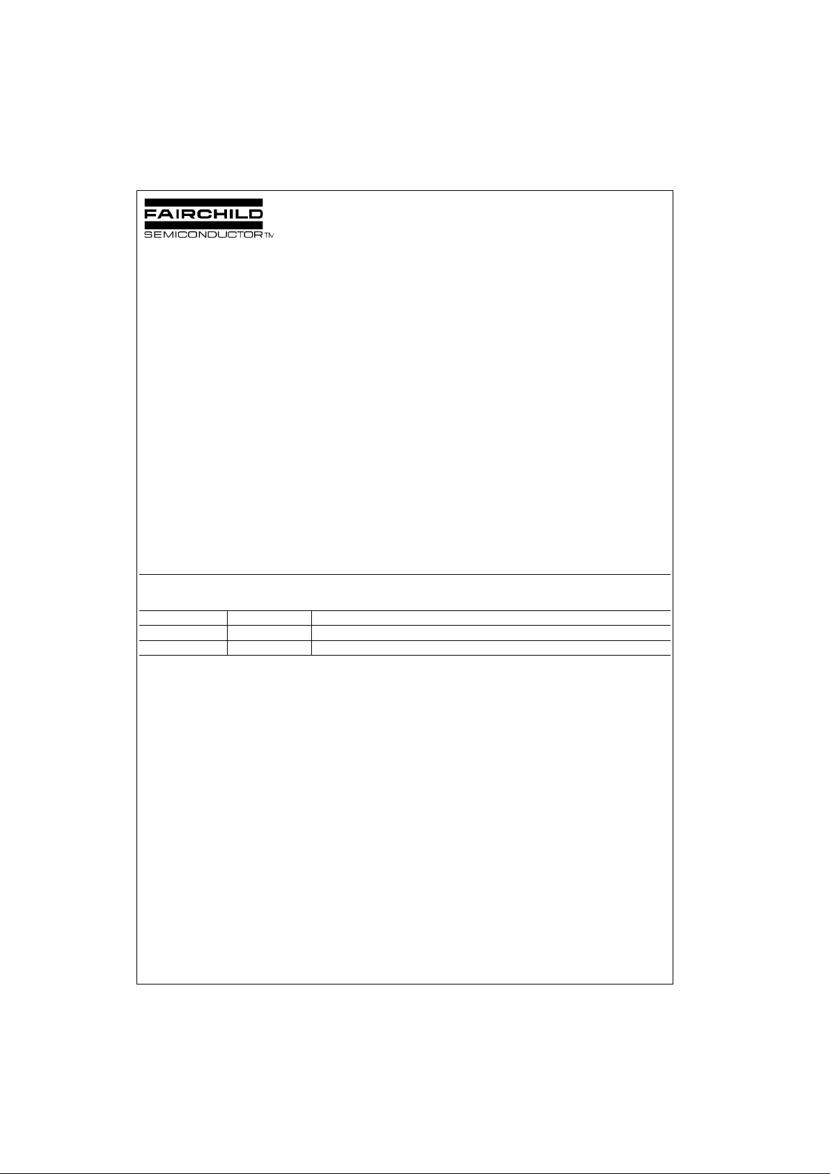
Pin Descriptions Connection Diagram
Truth Table
(Note 1)
Note 1: A-to-B data flo w is sh ow n. B-to-A data flow is similar but uses OEBA, LE BA, CLKBA, and CEBA.
Note 2: Output level before the indicated s t eady state input conditions were established , provided that CLKAB w as H IG H before LEAB went LOW.
Note 3: Output level before the indicated steady-state input conditions were established.
Pin Names Description
OEAB
A-to-B Output Enable
(Active LOW) (LVTTL levels)
OEBA
B-to-A Output Enable
(Active LOW) (LVTTL levels)
CEAB
A-to-B Clock/LE Enable
(Active LOW) (LVTTL levels)
CEBA
B-to-A Clock/LE Enable
(Active LOW) (LVTTL levels)
LEAB A-to-B Latch Enable
(Transparent HIGH) (LVTTL levels)
LEBA B-to-A Latch Enable
(Transparent HIGH) (LVTTL levels)
V
REF
GTLP Input Threshold
Reference Voltage
CLKAB A-to-B Clock (LVTTL levels)
CLKBA B-to-A Clock (LVTTL levels)
A1–A17 A-to-B Data Inputs or
B-to-A 3-STATE Outputs
B1–B17 B-to-A Data Inputs or
A-to-B Open Drain Outputs (GTLP Levels)
CLKIN B-to-A Buffered Clock Output
(LVTTL levels)
CLKOUT GTLP Buffered Clock Input/Output of CLK AB
(GTLP Levels)
Inputs Output
B
Mode
CEAB
OEAB LEAB CLKAB A
X H X XXZ Latched
LLLH or LXB
0
(Note 2) storage
LLLH or LXB
0
(Note 3) of A data
X L H X L L Transparent
XLHXHH
LLL↑ L L Clocked
LLL↑ H H storage
of A data
HLLXXB
0
(Note 3) Clock inhibit
Page 3
3 www.fairchildsemi.com
GTLP17T616
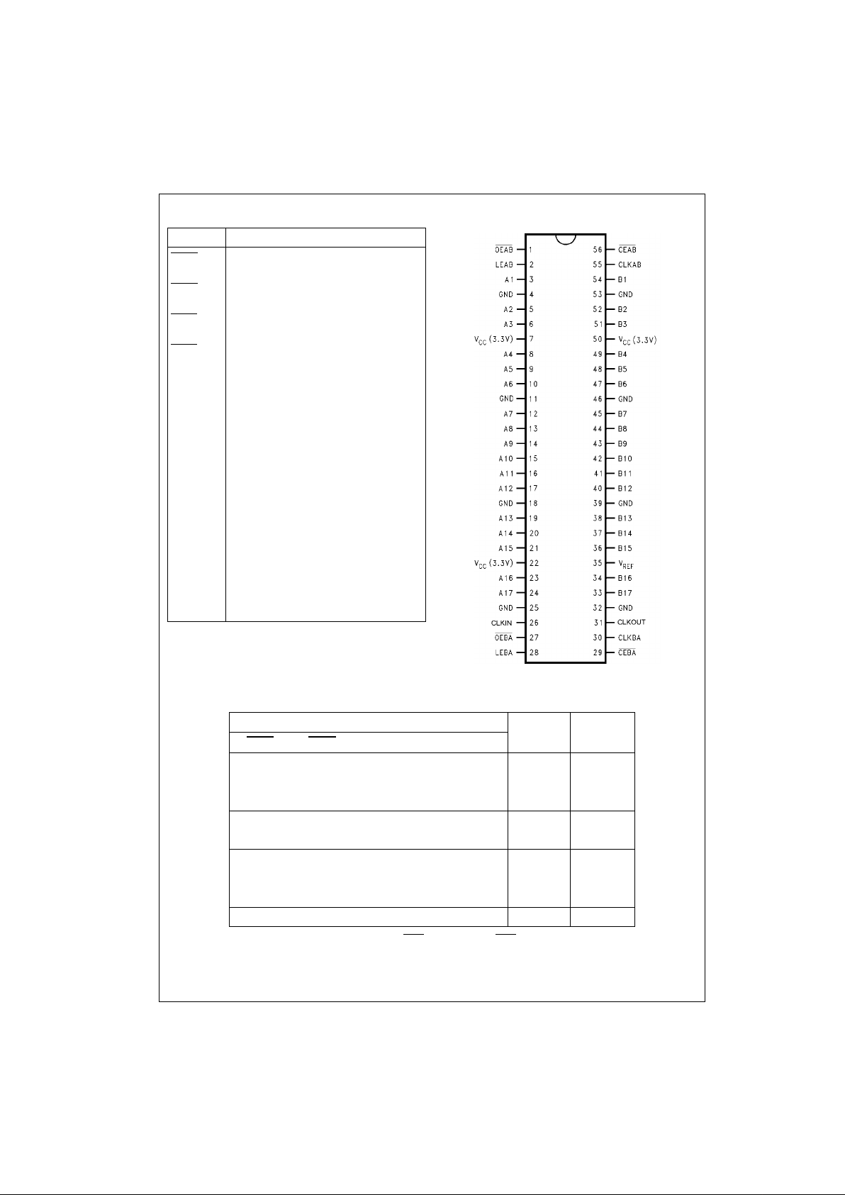
Functional Description
The GTLP17T616 is a 17 bit registered transceiver containing D-type flip-flop, latch and transparent modes of operation for
the data path and a GTLP translation of the CLKAB signal (CLKOUT). Data flow in each direction is controlled by the clock
enables (CEAB
and CEBA), latch enables (LEAB and LEBA), clock (CLKAB and CLKBA) and output enables (OEAB and
OEBA
). The clock enables (CEAB and CEBA) enable all 17 bits. The output enables (OEAB and OEBA) control the 17 bits
of data and the CLKOUT/CLKIN buffered clock path. For A-to-B data flow, when CEAB
is low, the device operates on the
LOW-to-HIGH transition of CLKAB for the flip-flop and on the HIGH-to-LOW transition of LEAB for the latch path. That is, if
CEAB
is LOW and LEAB is LOW the A data is latched regardless as to the state of CLKAB (HIGH or LOW) and if LEAB is
HIGH the device is in transparent mode. When OEAB
is LOW the outputs are active. When OEAB is HIGH the outputs are
high impedance. The data flow of B-to-A is similar except that CEAB
, OEBA, LEBA and CLKBA are used.
Logic Diagram
Page 4

www.fairchildsemi.com 4
GTLP17T616
Absolute Maximum Ratings(Note 4) Recommended Operating
Conditions
Note 4: Absolute Maximum continuous ratings are those values beyond
which damage to the device may occur. Exposure to these conditions or
conditions beyon d those indicated ma y adversely affect dev ice reliability.
Functional operation under absolute maximum rated conditions in not
implied.
Note 5: I
O
Absolute Maximum Rating must be observed.
DC Electrical Characteristics
Over Recommended Operating Free-Air Temperature Range, V
REF
= 1.0V (unless otherwise noted).
Supply Voltage (VCC) −0.5V to +4.6V
DC Input Voltage (V
I
) −0.5V to +4.6V
DC Output Voltage (V
O
)
Outputs 3-STATE −0.5V to +4.6V
Outputs Active (Note 5) −0.5V to +4.6V
DC Output Sink Current into
A Port I
OL
48 mA
DC Output Source Current from
A Port I
OH
−48 mA
DC Output Sink Current into
B Port in the LOW State, I
OL
100 mA
DC Input Diode Current (I
IK
)
V
I
< 0V −50 mA
DC Output Diode Current (I
OK
)
V
O
< 0V −50 mA
ESD Rating >2000V
Storage Temperature (T
STG
) −65°C to +150°C
Supply Voltage V
CC/VCCQ
3.15V to 3.45V
Bus Termination Voltage (V
TT
)
GTLP 1.47V to 1.53V
V
REF
0.98V to 1.02V
Input Voltage (V
I
)
on A Port and Control Pins 0.0V to V
CC
on B Port 0.0V to V
CC
HIGH Level Output Current (IOH)
A Port −24 mA
LOW Level Output Current (I
OL
)
A Port +24 mA
B Port +50 mA
Operating Temperature (T
A
) −40°C to +85°C
Symbol Test Conditions Min
Typ
Max Units
(Note 6)
V
IH
B Port V
REF
+ 0.05 V
TT
V
Others 2.0
V
IL
B Port 0.0 V
REF
− 0.05
V
Others 0.8
V
REF
B Port VTT > V
REF
+ 50 mV 0.25 1.0 VCC − 1.2V V
V
TT
B Port VTT > V
REF
+ 50 mV V
REF
+ 50 mV 1.5 V
CC
V
IK
VCC = 3.15V II = −18 mA −1.2 V
V
OH
A Port VCC = Min to Max (Note 7) IOH = −100 µAV
CC
–0.2
VVCC = 3.15V IOH = −18 mA 2.4
IOH = -24mA 2.2
V
OL
A Port VCC = Min to Max (Note 7) IOL = 100 µA0.2
V
VCC = 3.15V IOL = 24mA 0.5
B Port VCC = 3.15V IOL = 40 mA 0.4
V
IOL = 50 mA 0.55
I
I
Control Pins VCC = Min to Max (Note 7) VI = 3.45V or 0V ±5 µA
A Port VCC = 3.45V VI = 3.45V or 0V ±10 µA
B Port VCC = 3.45V VI = 0 to 3.45V ±5 µA
I
PU/PD
All Ports VCC = 0 to 1.5V VI/VO = 0 to 3.45V ±30 µA
I
OFF
All Ports VCC = 0V
I
or VO = 0 to 3.45V 30 µA
I
I(hold)
A Port VCC = 3.15V VI = 0.8V 75
µA
VI = 2.0V −75
I
OZH
A Port VCC = 3.45V VO = 3.45V 10
µA
B Port VO = 1.5V 5
I
OZL
A Port VCC = 3.45V VO = 0V −10
µA
B Port VO = 0.55V −5
ICC A or B Ports VCC = 3.45V Outputs HIGH 45
mA(VCC/V
CCQ
)I
O
= 0 Outputs LOW 45
VI = VCC or GND Outputs Disabled 45
∆I
CC
A Port and VCC = 3.45V,
One Input at 2.7V 0 2 mA
(Note 8) Control Pins A or Control Inputs at VCC or GND
Page 5

5 www.fairchildsemi.com
GTLP17T616
DC Electrical Characteristics (Continued)
Note 6: All typical value s are at VCC = 3.3V, V
CCQ
= 3.3V, and TA = 25°C.
Note 7: For conditions s hown as Min or Max, use the appropriate value specified under recomm ended operating conditions.
Note 8: This is the increas e in supply current for eac h input that is at the specif ied TTL voltage level rath er than V
CC
or GND.
AC Operating Requirements
Over recommended ranges of supply voltage and operating free-air temperature, V
REF
= 1.0V (unless otherwise noted).
Symbol Test Conditions Min
Typ
Max Units
(Note 6)
C
i
Control Pins VI = VCC or 0 5.0
A Port VI = VCC or 0 7.0 pF
B Port VI = VCC or 0 9.0
Symbol Test Conditions Min Max Unit
f
TOGGLE
Max Toggle Frequency Transparent Mode 125
MHz
f
MAX
Max Clock Frequency Registered Mode 125
t
WIDTH
Pulse Duration LEAB or LEBA HIGH 3.0
ns
CLKAB or CLKBA HIGH or LOW 3.0
t
SU
Setup Time A before CLKAB↑ 0.6
ns
B before CLKBA↑ 1.2
A before LEAB↑ 0.5
B before LEBA↑ 1.3
CEAB before CLKAB↑ 1.4
CEBA before CLKBA↑ 1.2
t
HOLD
Hold Time A after CLKAB↑ 0
ns
B after CLKBA↑ 0.2
A after LEAB↑ 0.2
B after LEBA↑ 0
CEAB after CLKAB↑ 0.5
CEBA after CLKBA↑ 0.6
Page 6

www.fairchildsemi.com 6
GTLP17T616
AC Electrical Characteristics
Over recommended range of supply voltage and operating free-air temperature, V
REF
= 1.0V (unless otherwise noted).
CL = 30 pF for B Port and CL = 50 pF for A Port.
Note 9: All typical va lues are at VCC = 3.3V, and TA = 25°C.
Symbol
From To
Min
Typ
Max Unit
(Input) (Output) (Note 9)
t
PLH
AB1.64.06.3
ns
t
PHL
1.0 2.5 4.4
t
PLH
LEAB B 1.5 3.9 6.3
ns
t
PHL
0.9 2.3 4.2
t
PLH
CLKAB B 1.6 4.0 6.3
ns
t
PHL
1.0 2.4 4.0
t
PLH
CLKAB CLKOUT 2.6 5.2 7.7
ns
t
PHL
1.7 3.4 6.0
t
PLH
OEAB B or CLKOUT 1.1 4 .3 6 . 5
ns
t
PHL
1.0 2.0 4.3
t
RISE
Transition time, B outputs (20% to 80%) 2.3
ns
t
FALL
Transition time, B outputs (80% to 20%) 1.6
t
RISE
Transition Time, A outputs (10% to 90%) 2.3
ns
t
FALL
Transition Time, A outputs (90% to 10%) 2.3
t
PLH
BA1.72.94.5
ns
t
PHL
1.7 3.2 5.8
t
PLH
LEBA A 0.3 2.5 4.6
ns
t
PHL
0.4 2.5 4.6
t
PLH
CLKBA A 0.5 2.6 4.6
ns
t
PHL
0.6 2.8 4.6
t
PLH
CLKOUT CLKIN 1.2 2.4 5.3
ns
t
PHL
2.2 3.5 5.3
t
PZH
, t
PZL
OEBA A or CLKIN 0.3 2.8 5.2
ns
t
PHZ
, t
PLZ
0.3 2.5 5.2
Page 7

7 www.fairchildsemi.com
GTLP17T616
AC Extended Electrical Characteristics
Over recommended ranges of supply voltage and operating free-air temperature V
REF
= 1.0V (unless otherwise noted).
C
L
= 30 pF for B Port and CL = 50 pF for A Port.
Note 10: All typical valu es are at VCC = 3.3V, and TA = 25°C.
Note 11: t
OSHL/tOSLH
and t
OST
- Output to output skew is defined as the absolute value of the difference between the actual propagation delay for all outputs
within the same packaged device. T he specifications a re given for specif ic w orst case V
CC
and temperature and apply to any outputs switching in the same
direction either HIGH -to-LOW (t
OSHL
) or LOW-to-HIGH (t
OSLH
) or in opposite direct ions both HL and LH (t
OST
). This parameter is guaranteed by desi gn and
statistical process dis tributio n. Actua l skew v alues be tween t he GTLP outputs could vary on the backplan e due to t he loadin g and imp edanc e seen by t he
device.
Note 12: t
PV
- Part to part skew is defin ed as the absolute value of the difference between the ac tu al propagation delay fo r all outputs from device to device.
The parameter is specified for a specific worst case V
CC
and temperature. This parameter is guaranteed by design and statistical process distribution. Actual
skew values between the GTLP outputs could vary on the backplane due to the loading and impedance seen by t he device.
Note 13: Due to the open drain structure on GTLP outputs t
OST
and t
PV(LH)
in the A-to-B direction are not specified. Skew on these paths is dependent on the
V
TT
and RT values on the backplane.
Note 14: t
PDELLH
and t
PDELHL
-B to CLKOUT propagation delay delta is defined as the difference between the CLKAB to CLKOUT propagation delay and the
CLKAB to B propagation delays. This parameter is for a given device and is not meant to guarantee the delta between the CLKAB to CLKOUT propaga t ion
delays of one device and the CLKAB to B prop agation delays of other dev ices. This paramete r is guaranteed by design and statistical process dist ribution.
Symbol
From
(Input)
To
(Output)
Min
Typ
(Note 10)
Max Unit
t
OSLH
(Note 11) A B 0.3 1.0
ns
t
OSHL
(Note 11) 0.3 0.6
t
PVHL
(Note 12)(Note 13) A B 2.5 ns
t
OSLH
(Note 11) CLKAB B 0.3 1.0
ns
t
OSHL
(Note 11) 0.3 0.6
t
PVHL
(Note 12)(Note 13) CLKAB B 2.5 ns
t
OSLH
(Note 11) B A 0.3 0.5
ns
t
OSHL
(Note 11) 0.3 0.5
t
OST
(Note 11) B A 0.5 1.2 ns
tPV (Note 12) B A 2.5 ns
t
OSLH
(Note 11) CLKBA A 0.3 0.5
ns
t
OSHL
(Note 11) 0.3 0.5
t
OST
(Note 11) CLKBA A 0.5 1.2 ns
tPV (Note 12) CLKBA A 2.5 ns
t
PVHL
(Note 11)(Note 12) CLKAB CLKOUT 2.8 ns
t
PDELLH
(Note 14) B CLKOUT 0 1.7
ns
t
PDELHL
(Note 14) 0 1.5
Page 8

www.fairchildsemi.com 8
GTLP17T616
Test Circuits and Timing Waveforms
Test Circuit for A Outputs
Note A: CL includes probes and Jig capacitance.
Test Circuit for B Outputs
Note B: For B Port, CL = 30 pF is used for wors t cas e.
Voltage Waveform - Propagation Delay Times Voltage Waveform - Pulse Width
Voltage Waveform - Setup and Hold Times Voltage Waveform Enable and Disable times
Output Waveform 1 is for an out put with intern al conditio ns such that the
output is LOW excep t when disabled by the control output.
Output Waveform 2 is for an out put with intern al conditio ns such that the
output is HIGH excep t wh en disabled by the cont rol output.
Input and Measure Conditions
All input pulses have the following characteristics: Frequency = 10MHz, t
RISE
= t
FALL
= 2 ns (10% to 90%), ZO = 50Ω
The outputs are measured one at a time wi th one transition per meas urement.
Test S
t
PLH/tPHL
OPEN
t
PLZ/tPZL
6V
t
PHZ/tPZH
GND
A or LVTTL
Pins
B or GTLP
Pins
V
inHIGH
V
CC
1.5
V
inLOW
0.0 0.0
V
M
VCC/2 1.0
V
X
VOL + 0.3V N/A
V
Y
VOH − 0.3V N/A
Page 9

9 www.fairchildsemi.com
GTLP17T616
Physical Dimensions inches (millimeters) unless otherwise noted
56-Lead Shrink Small Outline Package (SSOP), JEDEC MO-118, 0.300” Wide
Package Number MS56A
Page 10

www.fairchildsemi.com 10
GTLP17T616 17-Bit LVTTL/GTLP Bus Transceiver with Buff ered Clock
Physical Dimensions inches (millimeters) unless otherwise noted (Continued)
56-Lead Thin Shrink Small Outline Package (TSSOP), JEDEC MO-153, 6.1mm Wide
Package Number MTD56
Fairchild does not assume any responsibility for use of any circuitry described, no circuit pate nt licenses are implied and
Fairchild reserves the right at any time without notice to change said circuitry and specifications.
LIFE SUPPORT POLICY
FAIRCHILD’S PRODUCTS ARE NOT AUTHORIZED FOR USE AS CRITICAL COMPONENTS IN LIFE SUPPORT
DEVICES OR SYSTEMS WITHOUT THE EXPRESS WRITTEN APPROVAL OF THE PRESIDENT OF FAIRCHILD
SEMICONDUCTOR CORPORATION. As used herein:
1. Life support devices or systems are devices or syste ms
which, (a) are intended for surgical implant into the
body, or (b) support or sustain life, and (c) whose failure
to perform when properly used in accordance with
instructions for use provided in the labeling, can be reasonably expected to result in a significant inju ry to the
user.
2. A critical component i n any compon ent of a lif e support
device or system whose failu re to perform can be reasonably expected to ca use the fa i lure of the life su pp ort
device or system, or to affect its safety or effectiveness.
www.fairchildsemi.com
 Loading...