

Page 1

© 2000 Fairchild Semiconductor Corporation DS500172 www.fairchildsemi.com
August 1998
Revised April 2000
GTLP16T1655 16-Bit LVTTL/GTLP Universal Bus Transceiver
GTLP16T1655
16-Bit LVTTL/GTLP Universal Bus Transceiver
General Description
The GTLP16T1655 is a 16-bit universal bus transceiver
that provides LVTTL to GTLP signal level translation. It
allows for transparent, latched and clocked modes of data
transfer. The device provides a high speed interface
between cards operating at LVTTL logic levels and a ba ckplane operating at GTLP logic levels. High speed backplane operation is a direct re sult of GTLP’s reduced output
swing (<1V), reduced input threshold levels and output
edge rate control. The edge rate control minimizes bus settling time. GTLP is a Fair child Semico nductor der ivative of
the Gunning Transceiver Logic (GTL) JEDEC standard
JESD8-3.
Fairchild’s GTLP has intern al edge-r ate cont rol and is process, voltage, and temperature (PVT) compensated. Its
function is similar to BTL and GT L but with different outp ut
levels and receiver threshold. GTLP output LOW level is
typically less than 0. 5V, the output level HIGH i s 1.5V a nd
the receiver threshold is 1.0V.
Features
■ Bidirectional interface between GTLP and LVTTL logic
levels
■ Variable Edge Rate Control pin t o select desired edge
rate on the GTLP backplane (V
ERC
)
■ Partitioned as two 8-Bit transce iv ers wi th indivi du al latch
timing and output control but with a common clock.
■ Power up/down high impedance for live insertion.
■ External pin to pre-condition I/O capacitance to high
state
■ Bus-hold data inputs on the A-Port eliminates the need
for external pull-up resistors on unused inputs
■ LVTTL compatible driver and control inputs
■ Flow through pinout optimizes PCB layout
■ Open drain on GTLP to support wired-or connection
■ A Port source/sink −24 mA/+24 mA
■ B Port sink +100mA
■ D-type flip-flop, latch and transparent data paths
■ −40°C to 85°C Temperature capability
■ Available in TSSOP
Ordering Code:
Devices also availab le in Tape and Reel. Specify by appending th e s uffix let t er “X” to the ordering code.
Order Number Package Number Package Description
GTLP16T1655MTD MTD64 64-Lead Thin Shrink Small Outline Package, JEDEC MO-153, 6.1mm Wide
Page 2

www.fairchildsemi.com 2
GTLP16T1655
Connection Diagram Pin Descriptions
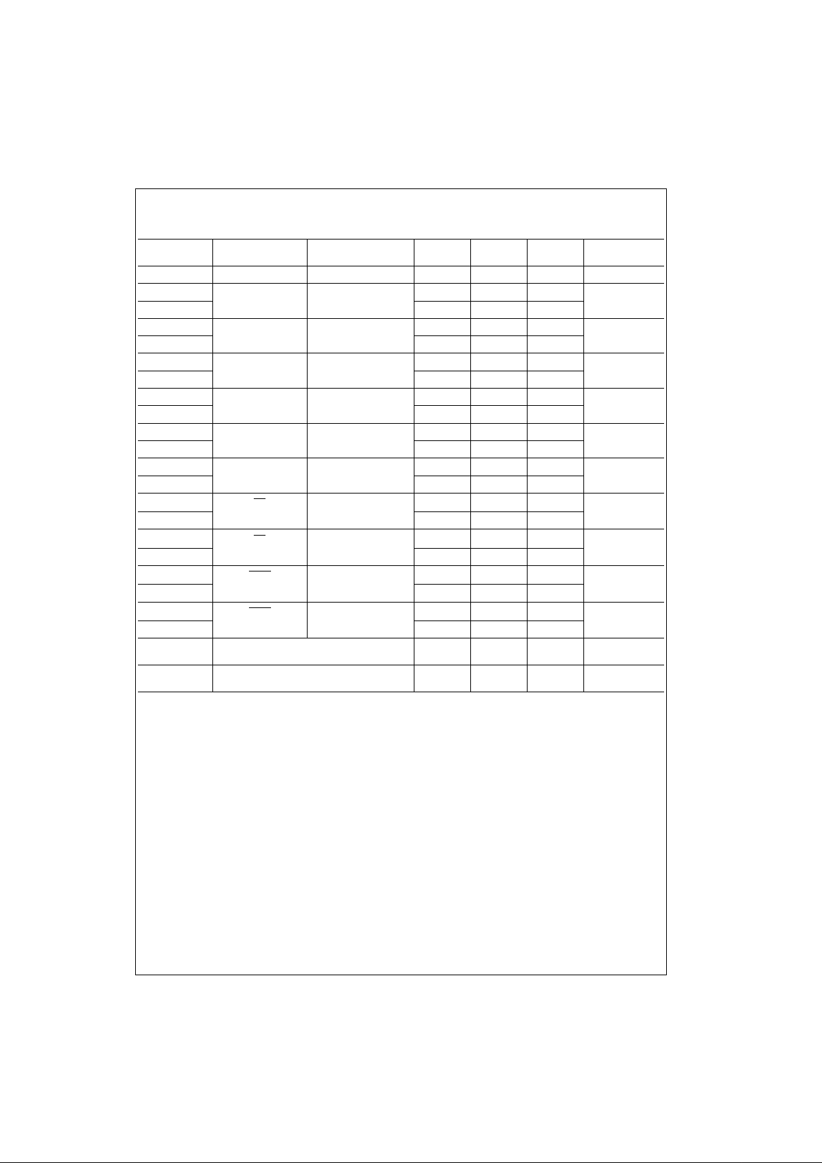
Truth Tables
(Note 1)
Note 1: A-to-B data flow is shown. B-to-A data flow is similar but uses OEBA, LEBA, CLK.
Note 2: Output level before the indicated steady state input conditions were es ta blished, provided CLK wa s H IG H prior to LEAB going LOW.
Note 3: Output level before the indicated steady state input conditions were es ta blished.
Pin Names Description
1OEAB A-to-B Output Enable (Active LOW)
2OEAB
Byte 1 and Byte 2
1OEBA B-to-A Output Enable (Active LOW)
2OEBA
Byte 1 and Byte 2
OE Disables all I/O ports simultaneously
1LEAB A-to-B Latch Enable (Transparent HIGH)
2LEAB Byte 1 and Byte 2
1LEBA B-to-A Latch Enable (Transparent HIGH)
2LEBA Byte 1 and Byte 2
V
REF
GTLP Reference Voltage
CLK A-to-B and B-to-A Clock
1A1-1A8 A Port I/O Byte 1 and Byte 2
2A1-2A8
1B1-1B8 B Port I/O Byte 1 and Byte 2
2B1-2B8
Inputs
Output
B
Mode
CEAB LEAB CLK A
H X X X Z High Impedance
L H X L L Transparent
L H X H H Transparent
LL↑ L L Registered
LL↑ H H Registered
LLHXB
0
(Note 2) Previous State
LLLXB
0
(Note 3) Previous State
Inputs Outputs Inputs Output Edge
OE
OEAB OEBA A Port B Port
V
ERC
B Port
LLLActiveActive V
CC
Slow
L L H Z Active GND Fast
LHLActiveZ
LHHZZ
HXXZZ
Page 3

3 www.fairchildsemi.com
GTLP16T1655
Functional Description
The GTLP16T1655 is a hig h drive (100 mA ) 16-bit univ ersal bus transceiver containing D-type flip-flop, latch and
transparent modes of operation for the data path. The
device is uniquely part ition ed as two 8-bit transceivers wi th
individual latch timin g and output contro l signa ls but w ith a
common clock pin (CLK) for both transceiver words. Da ta
flow for each word i s determined by the respecti ve latch
enables (xLEAB and xLEBA), output enables (xOEAB
and
xOEBA
) and clock (CLK). The output enables (1OEAB,
1OEBA
, and 2OEAB and 2OEBA) control Byte1 and Byte2
data for the A to B and B to A directions respectively.
For A-to-B data flow, the devices operate in the transparent
mode when LEAB is HIGH. When LEAB transitions LOW,
the A data is latched indepe ndent of CLK HIGH or LO W. If
LEAB is LOW the A data is registered on the CLK LOW-toHIGH transition. When OEAB
is LOW the outputs are
active. With OEAB
HIGH the outputs are HIGH impedance.
Data flow for the B-to-A direction is identical but uses
OEBA
, LEBA and CLK. Note that CLK is common to both
directions and both 8-bit w ords. OE
is also common and is
used to disable all I/O ports simultaneously.
Logic Diagrams
Page 4

www.fairchildsemi.com 4
GTLP16T1655
Absolute Maximum Ratings (Note 4) Recommended Operating
Conditions
Note 4: The Absolute Maximum Ratings are those values beyond which
the safety of the dev ice cannot be guaranteed. T he device sh ould not be
operated at these limit s. The parametric values defin ed in the Electrical
Characteristics tables are not guaranteed at the absolute maximum rating.
The “Recomme nded O peratin g Cond itions ” table will defin e the condition s
for actual device operation.
Note 5: I
O
Absolute Maximum Rating must be observed.
Note 6: V
TT
and R
term
can be adjusted t o accommodate bac k plane imped-
ances other than 50Ω, within the boundaries of not exceeding the DC
Absolute I
OL
ratings (200 mA). Simila rly V
REF
can be adjusted to compen-
sate for changes in V
TT
.
Supply Voltage (VCC) −0.5V to +4.6V
DC Input Voltage (V
I
) −0.5V to +4.6V
DC Output Voltage (V
O
)
Outputs 3-STATE −0.5V to +4.6V
Outputs Active (Note 5) −0.5V to + 4.6V
DC Output Sink Current into
A Port I
OL
48 mA
DC Output Source Current from
A Port I
OH
−48 mA
DC Output Sink Current
into B Port in the LOW State, I
OL
(Note 6) 200 mA
DC Input Diode Current (I
IK
)
V
I
< 0V −50 mA
DC Output Diode Current (I
OK
)
V
O
< 0V −50 mA
V
O
> V
CC
+50 mA
ESD Rating >2000V
Storage Temperature (T
STG
) −65°C to +150°C
Supply Voltage V
CC
3.0V to 3.6V
Bus Termination Voltage (V
TT
)
GTLP 1.35V to 1.65V
GTL 1.14V to 1.26V
V
REF
GTLP 0.87V to 1.1V
GTL 0.74V to 0.87V
Input Voltage (V
I
)
on A Port and Control Pins 0.0V to V
CC
on B Port 0.0V to V
tt
HIGH Level Output Current (IOH)
A Port −24 mA
LOW Level Output Current (I
OL
)
A Port +24mA
B Port +100 mA
Operating Temperature (T
A
) −40°C to +85°C
Page 5

5 www.fairchildsemi.com
GTLP16T1655
DC Electrical Characteristics
Over Recommended Operating Free-Air Temperature Range, V
REF
= 1.0V (unless otherwise noted).
Note 7: All typical values are at VCC = 3.3V, and TA = 25°C.
Note 8: For conditions shown as Min or Max, use the appropriate value specified under recommended operating conditions.
Note 9: This is specified by characterization but not tested.
Note 10: This is the increase in supply current fo r each input that is at the spe ci fie d T T L voltage level rather than V
CC
or GND.
Symbol Test Conditions Min
Typ
(Note 7)
Max Units
V
IH
B Port V
REF
+0.05 V
TT
V
Others 2.0 V
V
IL
B Port 0.0 V
REF
−0.05 V
Others 0.8 V
V
REF
GTLP 0.74 1.0 1.1 V
V
IK
VCC = 3.0V II = −18 mA −1.2 V
V
OH
A Port VCC = Min to Max (Note 8) IOH = −100 µAV
CC
−0.2
V
CC
= 3.0V IOH = −12 mA 2.4 V
I
OH
= −24 mA 2.2
V
OL
A Port VCC = Min to Max (Note 8) IOL = 100 µA0.20
VV
CC
= 3.0V IOL = 12 mA 0.40
I
OL
= 24 mA 0.50
B Port V
CC
= 3.0V IOL = 40 mA 0.20 V
IOL = 80 mA 0.40
IOL = 100 mA 0.50
I
I
A Port VCC = 3.6V VI = VCC or 0V ±10 µA
Control Pi ns VCC = 3.6V VI = VCC or 0V ±10 µA
B Port V
CC
= 3.6V VI = VTT or GND ±10 µA
I
OFF
Except VCC = 0V
I
or VO = 0 to 100
µA
V
ERC
V
CC
I
I(hold)
A Port VCC = 3.0V VI = 0.8V 75
µAVI = 2.0V −75
VCC = 3.6V VI = 0 to V
CC
±500
I
OZH
A Port VCC = 3.6V VO = V
CC
10
µA
B Port VO = 1.5V 10
I
OZL
A Port VCC = 3.6V VO = 0V −10
µA
B Port V
O
= 0.4V −10
I
OZPU
A Port VCC = 0 to 1.5V VO = 0.5 to 3V ±50 µA
(Note 9) OE = 0 or V
CC
I
OZPD
A Port VCC = 1.5 to 0V VO = 0.5 to 3V ±50 µA
(Note 9) OE
= 0 or V
CC
I
CC
A or B Ports VCC = 3.6 Outputs HIGH 55
mA(v
cc
)I
O
= 0 Outputs LOW 55
V
I
= VCC or GND Outputs Disabled 55
∆I
CC
A Port and VCC = 3.6V One Input at 0 1
mA (Note 10) Control Pins A or Control VCC–0.6
Inputs at VCC or GND
C
i
Control Pi ns VI = VCC or 0 5.8 7.0
A Port VI = VCC or 0 8.0 9.5 pF
B Port VI = VCC or 0 8.3 9.9
Page 6

www.fairchildsemi.com 6
GTLP16T1655
Live Insertion Characteristics
Over Recommended Operating Free-Air Temperature Range, V
REF
= 1.0V (unless otherwise noted).
AC Operating Requirements (GTLP)
Over recommended ranges of supply voltage and operating free-air temperature, VTT = 1.5V and V
ref
= 1.0V (unless otherwise noted).
B to A AC Electrical Characteristics (GTLP)
Over recommended range of supply voltage and operating free-air temperature, V
REF
= 1.0V, VTT = 1.5V, V
ERC
=VCC or GND (unless ot he r -
wise noted). CL = 30 pF for B-Port and CL = 50 pF for A-Port.
Note 11: All typical values are at VCC = 3.3V, and TA = 25°C.
Parameter Test Conditions Min Typ Max Units
I
CC
B Port VCC = 0 to 3V VO = 0 to 1.2V 5 mA
(V
CC
BIAS) VCC = 3.0 to 3.6V VI (VCCBIAS) = 3 to 3.6V 10 µA
V
O
B Port V
CC
= 0VI (VCCBIAS) = 3.3v 1.1 V
I
O
B Port VCC = 0VI (VCCBIAS) = 3 to 3.6V VO = 0.4 −1
µAVCC = 0 to 3.6V OE = 3.3V 100
V
CC
= 0 to 1.5V OE = 0 to 3.3V 100
Parameter Min Max Unit
f
CLOCK
Max Clock Frequency 0160MHz
t
WIDTH
Pulse Duration LE HIGH 3.0
ns
CLK HIGH or LOW 3.0
t
SU
Setup Time Data before CLK↑ 2.5
ns
Data before LE↓ (CLK = X) 2.5
t
HOLD
Hold Time Data after CLK↑ 0.5
ns
Data after LE↓ (CLK = X) 0.5
Parameter
From
(Input)
To
(Output)
Min
Typ
(Note 11)
Max Unit
f
MAX
160 MHz
t
PLH
BA1.04.7
ns
t
PHL
1.5 4.8
t
PLH
LEAB A 1.2 4.0
ns
t
PHL
1.2 3.8
t
PLH
CLK A 1.2 4.0
ns
t
PHL
1.2 4.0
t
PLZ/HZ
OE A1.44.5
ns
t
PZH/ZL
1.0 4.0
t
PLZ/HZ
OEBA A1.24.9
ns
t
PZH/ZL
1.0 4.0
Page 7
7 www.fairchildsemi.com
GTLP16T1655
A to B AC Electrical Characteristics (GTLP)
Over recommended range of supply voltage and operating free air temperature, V = 1.0V, VTT = 1.5V (unless otherwise noted). CL = 30 pF for
B-Port and C
L
= 50 pF for A-Port.
Note 12: All Typical values are at VCC = 3.3V and TA = 25°C
Symbol
From
(Input)
To
(Output)
Min
Type
(Note 12)
Max Units
f
MAX
160 MHz
t
PLH
AB2.6 5.7
ns
t
PHL
V
ERC
= V
CC
0.8 4.5
t
PLH
AB2.0 4.9
ns
t
PHL
V
ERC
= GND 0.7 4.0
t
PLH
LEAB B 2.6 5.7
ns
t
PHL
V
ERC
= V
CC
0.8 4.0
t
PLH
LEAB B 2.2 4.9
ns
t
PHL
V
ERC
= GND 0.7 4.0
t
PLH
CLK B 2.8 5.7
ns
t
PHL
V
ERC
= V
CC
1.0 4.0
t
PLH
CLK B 2.3 5.0
ns
t
PHL
V
ERC
= GND 0.8 4.0
t
PLH
OE B2.7 5.8
ns
t
PHL
V
ERC
= V
CC
0.6 4.0
t
PLH
OE B2.1 4.9
ns
t
PHL
V
ERC
= GND 1.0 4.0
t
PLH
OEAB B2.6 5.8
ns
t
PHL
V
ERC
= V
CC
0.6 4.0
t
PLH
OEAB B2.0 4.9
ns
t
PHL
V
ERC
= GND 0.6 3.5
t
FALL/RISE
V
ERC
= V
CC
Transition Time, B outputs (0.6V to 1.3V) 0.7/0.7 2.0/2.5 ns
t
FALL/RISE
V
ERC
= GND
Transition Time, B outputs (0.6V to 1.3V) 0.7/0.7 1.5/2.0 ns
Page 8

www.fairchildsemi.com 8
GTLP16T1655
Extended Electrical Characteristics (GTLP)
Over recommended ranges of supply voltage and operating free-air temperature V
REF
= 1.0V (unless otherwise noted).
C
L
= 30 pF for B Port and CL = 50 pF for A Port.
Note 13: All typical values are at VCC = 3.3V, and TA = 25°C.
Note 14: t
OSHL/tOSLH
and t
OST
—Output to output skew is defined as the absolute value of the difference between the actual propagation delay for all outputs
within the same packaged device . T he specifications a re given for specific w orst case V
CC
and temperature and apply to an y outputs switching in the same
direction either HIGH-to-LOW (t
OSHL
) or LOW-to-HIGH (t
OSLH
) or in opposite directions both HL and LH (t
OST)
. This parameter is guaranteed by design and
statistical proces s distrib ution. Ac tual ske w values between the GT LP outp uts could vary on th e backpl ane du e to the load ing an d impedance seen by the
device.
Note 15: t
PV
—Part to part skew is define d as th e abs olute value of the difference bet w een the actual propagatio n delay for all outputs from device to device.
The parameter is specified for a specific worst case V
CC
and temperature. This parameter is guaranteed by design and statistical process distribution. Actual
skew values between the GTLP outputs could vary on the backplane due to the loading and impedance seen by the device.
Note 16: Due to the open drain st ructu re on GTL P out puts, t
OST
and t
PV(LH)
in the A-to-B directi on are n ot s pecifie d. Sk ew on the se pa ths is depen de nt on
the V
TT
and RT values on the backplane.
Symbol
From
(Input)
To
(Output)
Min
Typ
(Note 13)
Max Unit
t
OSLH
(Note 14) A B 0.4 1.0 ns
t
OSHL
(Note 14) 0.4 1.0 ns
t
PV(HL)
(Note 15) (Note 16) A B 1.5 ns
t
OSLH
(Note 14) CLKAB B 0.3 0.9 ns
t
OSHL
(Note 14) 0.3 0.6 ns
t
PV(HL)
(Note 15) (Note 16) CLKAB B 1.2 ns
t
OSLH
(Note 14) B A 0.3 1.0 ns
t
OSHL
(Note 14) 0.3 1.0 ns
t
OST
(Note 14) B A 0.6 1.5 ns
tPV (Note 15) B A 1.6 ns
t
OSLH
(Note 14) CLKAB A 0.3 0.6 ns
t
OSHL
(Note 14) 0.3 0.6 ns
t
OST
(Note 14) CLKAB A 0.5 1.0 ns
tPV (Note 15) CLKAB A 1.1 ns
Page 9

9 www.fairchildsemi.com
GTLP16T1655
AC Operating Requirements (GTL)
Over recommended ranges of supply voltage and operating free-air temperature, VTT = 1.2V and V
ref
= 0.8V (unless otherwise noted).
B to A AC Electrical Characteristics (GTL)
Over recommended range o f supply vol tage and o pera ti ng fr ee air tem pera ture, V
ref
= 0.8V , VTT = 1.2V, V
ERC
= VCC or GND (unless otherwise
noted). C
L
= 30pF for B Port and CL = 50 pF for A Port.
Note 17: All Typical values are at VCC = 3.3V and TA = 25°C.
Parameter Min Max Units
f
CLOCK
Max Clock Frequency 0 160 MHz
t
WIDTH
Pulse Duration LE HIGH 3.0 ns
CLK HIGH or LOW 3.0 ns
t
SU
Setup Time Data before CLK↑ 2.5
ns
Data before LE↓ (CLK = X) 2.5
t
HOLD
Hold Time Data after CLK↑ 0.5
ns
Data after LE↓ (CLK =X) 0.5
Parameter
From
(Input)
To
(Output)
Min
Typ
(Note 17)
Max Units
f
MAX
160 MHz
t
PLH
BA1.0 4.7
ns
t
PHL
1.2 4.8
t
PLH
LEBA A 1.0 4.4
ns
t
PHL
1.1 4.0
t
PLH
CLK A 1.0 4.2
ns
t
PHL
1.1 4.1
t
PLZ/HZ
OE A1.5 4.6
ns
t
PZH/ZL
1.2 4.2
t
PLZ/HZ
OEBA A1.2 4.9
ns
t
PZH/ZL
1.0 4.0
Page 10

www.fairchildsemi.com 10
GTLP16T1655
A to B AC Electrical Characteristics (GTL)
Over recommended range of supply voltage and operating free air temperature, V
REF
= 0.8V, VTT = 1.2V (unless otherwise noted).
C
L
= 30 pF for B Port and CL = 50 pF for A Port.
Note 18: All Typical values are at VCC = 3.3V and TA = 25°C.
Symbol
From
(Input)
To
(Output)
Min
Typ
(Note 18)
Max Units
f
MAX
160 MHz
t
PLH
AB2.25.7
ns
t
PHL
V
ERC
= V
CC
1.0 4.7
t
PLH
AB1.54.8
ns
t
PHL
V
ERC
= GND 0.9 4.0
t
PLH
LEAB B 2.2 5.7
ns
t
PHL
V
ERC
= V
CC
1.0 4.1
t
PLH
LEAB B 1.7 5.0
ns
t
PHL
V
ERC
= GND 0.9 4.4
t
PLH
CLK B 2.8 5.8
ns
t
PHL
V
ERC
= V
CC
1.0 4.3
t
PLH
CLK B 2.3 5.0
ns
t
PHL
V
ERC
= GND 1.0 4.3
t
PLH
OE B2.5 5.8
ns
t
PHL
V
ERC
= V
CC
0.8 4.3
t
PLH
OE B1.7 4.9
ns
t
PHL
V
ERC
= GND 0.9 4.3
t
PLH
OEAB B2.2 5.8
ns
t
PHL
V
ERC
= V
CC
0.8 4.3
t
PLH
OEAB B1.7 4.9
ns
t
PHL
V
ERC
= GND 0.9 3.8
t
FALL/RISE
V
ERC
= V
CC
Transition Time, B outputs (0.6V to 1.3V) 0.7/0.7 2.0/2.5
ns
t
FALL/RISE
V
ERC
= V
CC
Transition Time, B outputs (0.6V to 1.3V) 0.7/0.7 1.5/2.0
ns
Page 11

11 www.fairchildsemi.com
GTLP16T1655
Extended Electrical Characteristics (GTL)
Over recommended ranges of supply voltage and operating free-air temperature V
REF
= 0.8V (unless otherwise noted).
C
L
= 30 pF for B Port and CL = 50 pF for A Port.
Note 19: All typical valu es are at VCC = 3.3V, and TA = 25°C.
Note 20: t
OSHL/tOSLH
and t
OST
—Output to output skew is defined as the absolute value of the difference between the actual propagation delay for all outputs
within the same packaged device. T he specifications a re given for specific w orst case V
CC
and temperature and apply to an y outputs switching in the same
direction either HIGH-to-LOW (t
OSHL
) or LOW-to-HIGH (t
OSLH
) or in opposite directions both HL and LH (t
OST)
. This parameter is guaranteed by design and
statistical process distribution. Actual skew values between the GTL outputs could vary on the backplane due to the loading and impedanc e seen by t he
device.
Note 21: t
PV
—Part to part skew is defin ed as th e absolute value of the differenc e bet w een the actual propagatio n delay for all outputs from device to device.
The parameter is specified for a specific worst case V
CC
and temperature. This parameter is guaranteed by design and statistical process distribution. Actual
skew values between the GTL outputs could va ry on the backplane due to the loading and impedanc e seen by the device.
Note 22: Due to the open drain structure on GTL outputs, t
OST
and t
PV(LH)
in the A-to-B direction are not specified. Skew on these paths is dependent on the
V
TT
and RT values on the backplane.
Symbol
From
(Input)
To
(Output)
Min
Typ
(Note 19)
Max Unit
t
OSLH
(Note 20) A B 0.4 1.0 ns
t
OSHL
(Note 20) 0.4 1.0 ns
t
PV(HL)
(Note 21) (Note 22) A B 1.5 ns
t
OSLH
(Note 20) CLKAB B 0.3 0.9 ns
t
OSHL
(Note 20) 0.3 0.6 ns
t
PV(HL)
(Note 21) (Note 22) CLKAB B 1.2 ns
t
OSLH
(Note 20) B A 0.3 1.0 ns
t
OSHL
(Note 20) 0.3 1.0 ns
t
OST
(Note 20) B A 0.6 1.5 ns
tPV (Note 21) B A 1.6 ns
t
OSLH
(Note 20) CLKAB A 0.3 0.6 ns
t
OSHL
(Note 20) 0.3 0.6 ns
t
OST
(Note 20) CLKAB A 0.5 1.0 ns
tPV (Note 21) CLKAB A 1.1 ns
Page 12

www.fairchildsemi.com 12
GTLP16T1655
Test Circuits and Timing Waveforms
Test Circuit for A Outputs Test Circuit for B Outputs
Note A: CL includes probes and J ig capacitance.
Note B: For B-Port, C
L
= 30 pF is used fort worst case.
Voltage Waveform - Propagation Delay Times Voltage Waveform - Setup and Hold Times
Voltage Waveform - Pulse Width Voltage Waveform - Enable and Disable Times
Output Waveform 1 is for an output with internal conditions such that the
output is LOW excep t when disabled by the con tr ol output
Output Waveform 2 is for an output with internal conditions such that the
output is HIGH excep t wh en disabled by the control output
Input and Meas ure Conditions
All input pulses have the following characteristics: Frequency = 10MHz, t
RISE
= t
FALL
= 2 ns, ZO = 50Ω
The outputs are meas ured one at a time with on e tr ansition per measurement
Test S
t
PLH/tPHL
Open
t
PLZ/tPZL
6V
t
PHZ/tPZH
GND
A or LVTTL
Pins
B or GTLP
Pins
V
inHIGH
3.0 1.5
V
inLOW
0.0 0.0
V
M
1.5 1.0
V
X
VOL + 0.3V N/A
V
Y
VOH − 0.3V N/A
Page 13

13 www.fairchildsemi.com
GTLP16T1655
Physical Dimensions inches (millimeters) unless otherwise noted
64-Lead Thin S hrink Small Outlin e Package, JEDEC MO-153, 6.1mm Wide
Package Number MTD64
Page 14

www.fairchildsemi.com 14
GTLP16T1655 16-Bit LVTTL/GTLP Universal Bus Transceiver
Fairchild does not assume any responsibility for use of any circuitr y described, no circuit patent licenses are implied and
Fairchild reserves the right at any time without notice to change said circuitry and specifications.
LIFE SUPPORT POLICY
FAIRCHILD’S PRODUCTS ARE NOT AUTHORIZED FOR USE AS CRITICAL COMPONENTS IN LIFE SUPPORT
DEVICES OR SYSTEMS WITHOUT THE EXPRESS WRITTEN APPROVAL OF THE PRESIDENT OF FAIRCHILD
SEMICONDUCTOR CORPORATION. As used herein:
1. Life support devices or systems are devices or systems
which, (a) are intended for surgical implant into the
body, or (b) support or sustain life, and (c) whose failure
to perform when properly used in accordance with
instructions for use provided in the labeling, can be reasonably expected to result in a significant inju ry to the
user.
2. A criti cal com ponent in any com ponen t of a life supp ort
device or system whose failure t o perform can be reasonably expected to ca use the failure of the life supp ort
device or system, or to affect its safety or effectiveness.
www.fairchildsemi.com
 Loading...