

Datasheet GTLP16616MTDX, GTLP16616MTD, GTLP16616MEAX, GTLP16616MEA Datasheet (Fairchild Semiconductor)
Page 1
June 1997
Revised October 1998
GTLP16616 17-Bit TTL/GTLP Bus Transceiver with Buffered Clock
© 1998 Fairchild Semiconductor Corporation DS500017.prf www.fairchildsemi.com
GTLP16616
17-B
it TTL/GTLP Bus Transceiver
with Buffered Clock
General Description
The GTLP16616 i s a 1 7-bit r egist ered bus transc eiver th at
provides TTL to GTLP signal le vel translatio n. It al lows for
transparent, latched and clocked modes of dat a flow and
provides a buffered GTLP (CLKOUT) clock output from the
TTL CLKAB. The device p rovides a high speed interfa ce
between cards operating at TTL logic l evels and a backplane operating at GTLP logic levels. High speed back-
plane operation is a direct resu lt of GTLP’s red uced outp ut
swing (<1V), reduced input threshold levels and output
edge rate control. The edge rate control minimizes bus settling time. GTLP is a Fairchil d Semicondu ctor deriv ative of
the Gunning Transceiver logic (GTL) JEDEC standard
JESD8-3.
Fairchild’s GTLP has inter nal edg e-rate con trol and is process, voltage, and temperature (PVT) compensated. Its
function is similar to BTL and GT L but with different outp ut
levels and receiver threshold. GTLP output LOW level is
typically less than 0. 5V, the output level HIGH is 1.5V and
the receiver threshold is 1.0V.
Features
■ Bidirectional interface between GTLP and TTL logic
levels
■ Edge Rate Control to minimize noise on the GTLP port
■ Power up/down/off high impedance for live insertion
■ External V
REF
pin for receiver threshold
■ CMOS technology for low power dissipation
■ 5 V tolerant inputs and outputs on the A-Port
■ Bus-hold data inputs on the A-Port eliminates the need
for external pull-up resistors on unused inputs.
■ TTL compatible driver and control inputs
■ Flow through pinout optimizes PCB layout
■ Open drain on GTLP to support wired-or connection
■ A-port source/sink −32 mA/+32 mA
■ D-type flip-flop, latch and transparent data paths
■ GTLP Buffered CLKAB signal available (CLKOUT)
■ Recommended Operating Temperature −40°C to 85°C
Ordering Code:
Devices also availab le in Tape and Reel. Specify by appending su ffix let te r “X” to the ordering code .
Order Number Package Number Package Description
GTLP16616MEA MS56A 56-Lead Shrink Small Outline Package (SSOP), JEDEC MO-118 0.300” Wide
GTLP16616MTD MTD56 56-Lead Thin Shrink Small Outline Package (TSSOP), JEDEC MO-153, 6.1mm Wide
Page 2
www.fairchildsemi.com 2
GTLP16616
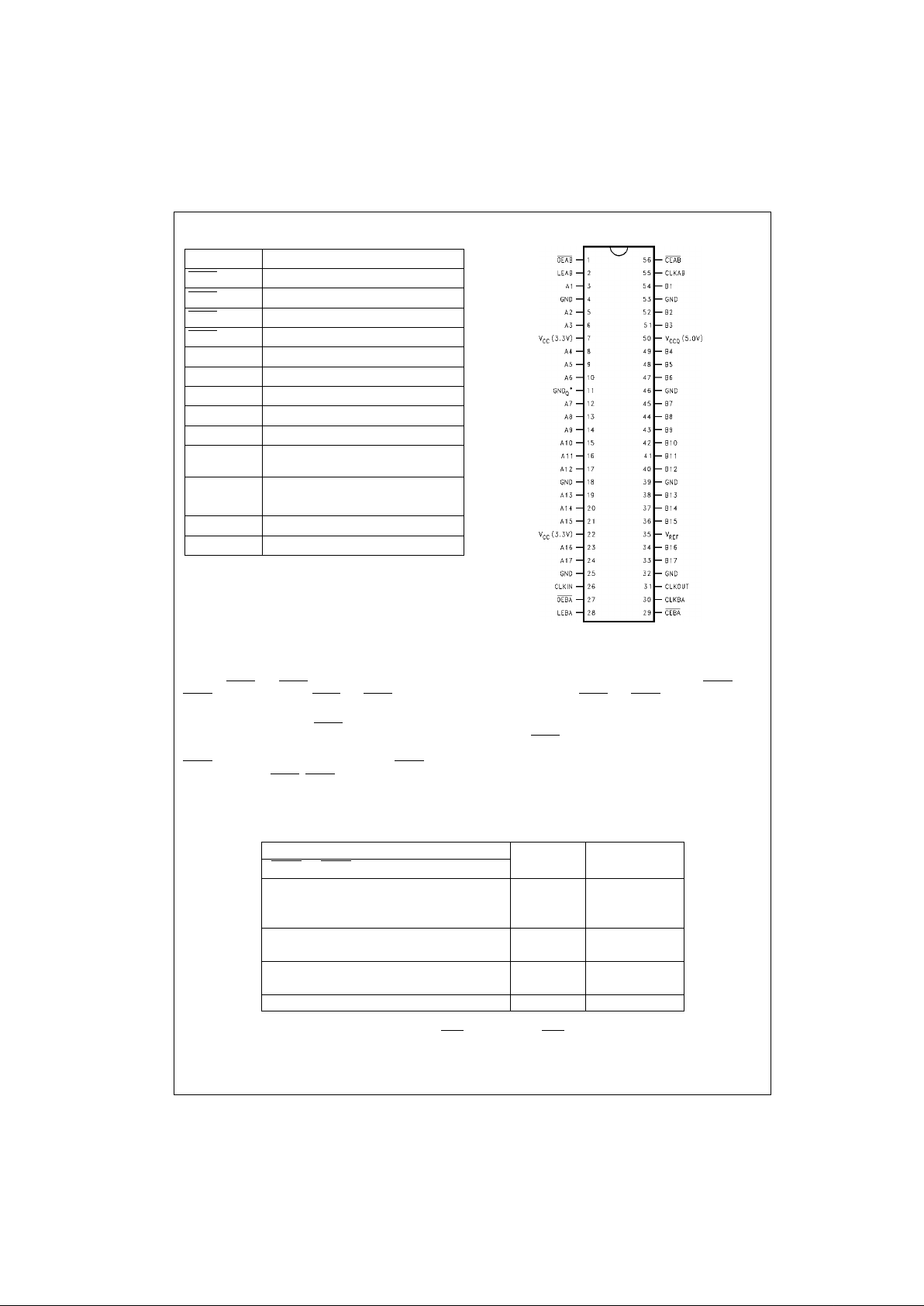
Pin Descriptions Connection Diagram
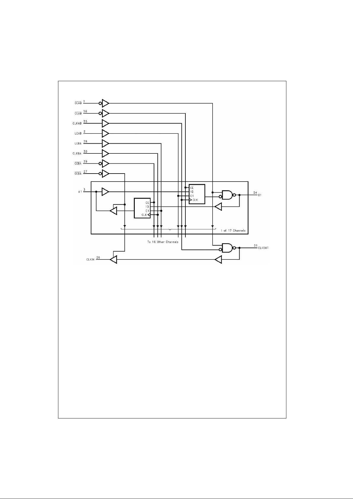
Functional Description
The GTLP16616 is a 17 bit re giste red transce iver co ntaining D-typ e flip-fl op, latch an d transp arent m odes of op eration for
the data path and a GTLP translation of the CLKAB signal (CLKOUT). Data flow in each direction is controlled by the clock
enables (CEAB
and CEBA), latch enables (LEAB and LEBA), clock (CLKAB and CLKBA) and output enables (OEAB and
OEBA
). The clock enables (CEAB and CEBA) enable all 17 bits. The output enables (OEAB and OEBA) control both the 17
bits of data and the CLKOUT/CLKIN buffered clock path.
For A-to-B data flow, when CEAB
is LOW, the device operates o n the LOW-to-HIGH tr ansition of C LKAB for the flip-flop
and on the HIGH-to-LOW transition of LEAB for the latch path. That is, if CEAB
is LOW and LEAB is LOW the A data is
latched regardless as to the state of CLKAB (HIGH or LOW) and if LEAB is HIGH the device is in transparent mode. When
OEAB
is LOW the outputs are active. When OEAB is HIGH the outputs ar e HIGH impedance . The data flow of B-to -A is
similar except that CEBA
, OEBA, LEBA and CLKBA are used.
Truth Table
(Note 1)
Note 1: A-to-B data flo w is sh ow n. B-to-A data flow is similar but uses OEBA, LE BA, CLKBA, and CEBA.
Note 2: Output level before the indicated s t eady-state input conditions were established, provided that CL KAB was HIGH prior to LEAB going LOW.
Note 3: Output level before the indicated steady-state input conditions were established.
Pin Names Description
OEAB
A-to-B Output Enable (Active LOW)
OEBA
B-to-A Output Enable (Active LOW)
CEAB
A-to-B Clock Enable (Active LOW)
CEBA
B-to-A Clock Enable (Active LOW)
LEAB A-to-B Latch Enable (Transparent HIGH)
LEBA B-to-A Latch Enable (Transparent HIGH)
V
REF
GTLP Reference Voltage
CLKAB A-to-B Clock
CLKBA B-to-A Clock
A1-A17 A-to-B Data Inputs or B-to-A 3-STATE
Outputs
B1-B17 B-to-A Data Inputs or
A-to-B Open Drain Outputs
CLKIN B-to-A Buffered Clock Output
CLKOUT GTLP Buffered Clock Output of CLKAB
Inputs Output
B
Mode
CEAB
OEAB LEAB CLKAB A
X H X X X Z Latched
LLLH or LXB
0
(Note 2) storage
LLLH or LXB
0
(Note 3) of A data
X L H X L L Transparent
XLHXH H
LLL↑ L L Clocked storage
LLL↑ H H of A data
HLLXXB
0
(Note 3) Clock inhibit
Page 3
3 www.fairchildsemi.com
GTLP16616
Logic Diagram
Page 4

www.fairchildsemi.com 4
GTLP16616
Absolute Maximum Ratings(Note 4) Recommended Operating
Conditions
(Note 6)
Note 4: The Absolute Maximum Ratings are those values beyond which
the safety of the dev ice cannot be guaranteed. T he device sh ould not be
operated at these limits. The parametric values defined in the Electrical
Characteristics tables are not guaranteed at the absolute maximum rating.
The “Recommend ed O peratin g Cond itions” t able w ill defin e the co ndition s
for actual device operation.
Note 5: I
O
Absolute Maximum Rating must be observed.
Note 6: Unused inputs must be held high or low.
Supply Voltage (VCC) −0.5V to +7.0V
DC Input Voltage (V
I
) −0.5V to +7.0V
DC Output Voltage (V
O
)
Outputs 3-STATE −0.5V to +7.0V
Outputs Active (Note 5) −0.5V to V
CC
+ 0.5V
DC Output Sink Current into
A-Port I
OL
64 mA
DC Output Source Current from
A-Port I
OH
−64 mA
DC Output Sink Current
into B-Port in the LOW State,
I
OL
80 mA
DC Input Diode Current (I
IK
)
V
I
< 0V −50 mA
DC Output Diode Current (I
OK
)
V
O
< 0V −50 mA
V
O
> V
CC
+50 mA
ESD Rating >2000V
Storage Temperature (T
STG
) −65°C to +150°C
Supply Voltage V
CC
V
CC
3.15V to 3.45V
V
CCQ
4.75V to 5.25V
Bus Termination Voltage (V
TT
) GTLP 1.35V to 1.65V
Input Voltage (V
I
)
on A-Port and Control Pins 0.0V to 5.5V
HIGH Level Output Current (I
OH
)
A-Port −32 mA
LOW Level Output Current (I
OL
)
A-Port +32 mA
B-Port +34 mA
Operating Temperature (T
A
) −40°C to +85°C
Page 5

5 www.fairchildsemi.com
GTLP16616
DC Electrical Characteristics
Over Recommended Operating Free-Air Temperature Range, V
REF
= 1.0V (unless otherwise noted).
Note 7: All typical value s are at VCC = 3.3V, V
CCQ
= 5.0V, and TA = 25°C.
Note 8: For conditions s hown as Min or Max, use the appropriate value s pecified under recomm ended operating conditions.
Note 9: This is the increas e in supply current for eac h input that is at the specif ied TTL voltage level ra th er than V
CC
or GND.
Symbol Test Conditions Min Typ Max Units
(Note 7)
V
IH
B-Port V
REF
+0.1 V
TT
V
Others 2.0 V
V
IL
B-Port 0.0 V
REF
−0.1 V
Others 0.8 V
V
REF
GTLP 1.0 V
GTL 0.8 V
V
IK
VCC = 3.15V, II = −18 mA −1.2 V
V
CCQ
= 4.75V
V
OH
A-Port VCC, V
CCQ
= Min to Max (Note 8) IOH = −100 µAV
CC
−0.2
VCC = 3.15V IOH = −8 mA 2.4 V
V
CCQ
= 4.75V IOH = −32 mA 2.0
V
OL
A-Port VCC, V
CCQ
= Min to Max (Note 8) IOL = 100 µA0.2V
VCC = 3.15V IOL = 32 mA 0.5
V
CCQ
= 4.75V
B-Port VCC = 3.15V V
CCQ
= 4.75V IOL = 34 mA 0.65 V
I
I
Control Pins VCC, V
CCQ
= 0 or Max VI = 5.5V or 0V ±10 µA
A-Port VCC = 3.45V VI = 5.5V 20
V
CCQ
= 5.25V VI = V
CC
1 µA
VI = 0 −30
B-Port VCC = 3.45V VI = V
CC
5 µA
V
CCQ
= 5.25V VI = 0 −5
I
OFF
A-Port and
Control Pins
VCC = V
CCQ
= 0V
I
or VO = 0 to 4.5V 100 µA
I
I(hold)
A-Port VCC = 3.15V, VI = 0.8V 75 µA
V
CCQ
= 4.75V VI = 2.0V −20
I
OZH
A-Port VCC = 3.45V, VO = 3.45V 1 µA
B-Port V
CCQ
= 5.25V VO = 1.5V 5
I
OZL
A-Port VCC = 3.45V, VO = 0 −20 µA
B-Port V
CCQ
= 5.25V VO = 0.65V −10
I
CCQ
(V
CCQ
)
A or B VCC = 3.45V, Outputs HIGH 30 40
mA
Ports V
CCQ
= 5.25V, Outputs LOW 30 40
IO = 0,
VI = V
CCQ
or GND Outputs Disabled 30 40
I
CC
(VCC)
A or B VCC = 3.45V, V
CCQ
= 5.25V, IO = 0, Outputs HIGH 0 1
Ports Outputs LOW 0 1 mA
VI = VCC or GND Outputs Disabled 0 1
∆I
CC
A-Port and VCC = 3.45V, One Input at 2.7V 0 1 mA
(Note 9) Control Pins VCC = 5.25V,
A or Control Inputs at
VCC or GND
C
IN
Control Pins VI = V
CCQ
or 0 8
C
I/O
A-Port VI = V
CCQ
or 0 9 pF
C
I/O
B-Port VI = V
CCQ
or 0 6
Page 6

www.fairchildsemi.com 6
GTLP16616
AC Operating Requirements
Over recommended ranges of supply voltage and operating free-air temperature, V
REF
= 1.0V (unless otherwise noted).
Symbol Min Max Unit
f
CLOCK
Max Clock Frequency 175 MHz
t
W
Pulse Duration LEAB or LEBA HIGH 3.0 ns
CLKAB or CLKBA HIGH or LOW 3.2
t
S
Setup Time A before CLKAB↑ 0.5 ns
B before CLKBA↑ 3.1
A before LEAB↓ 1.3
B before LEBA↓ 3.7
CEAB before CLKAB↑ 0.7
CEBA before CLKBA↑ 1.0
t
H
Hold Time A after CLKAB↑ 1.5 ns
B after CLKBA↑ 0.0
A after LEAB↓ 0.5
B after LEBA↓ 0.0
CEAB after CLKAB↑ 1.5
CEBA after CLKBA↑ 1.7
Page 7

7 www.fairchildsemi.com
GTLP16616
AC Electrical Characteristics
Over recommended range of supply voltage and operating free-air temperature, V
REF
= 1.0V (unless otherwise noted). CL = 30 pF for B-Port
and CL = 50 pF for A-Port.
Note 10: All typical valu es are at VCC = 3.3V, V
CCQ
= 5.0V, and TA = 25°C.
Note 11: Skew is defined as the abs olute value of the differ ence betw een the actua l propag ation delays for the C LKOUT pin and any B output transit ion
when measured with reference to CLKAB↑. This guarantees the relationsh ip between B output data and CLK OUT suc h that data is coincide nt or ahea d of
CLKOUT. This specification is guaranteed but not tested.
Symbol From To Min Typ Max Unit
(Input) (Output) (Note 10)
t
PLH
AB1.04.36.5ns
t
PHL
1.0 5.0 8.2
t
PLH
LEAB B 1.8 4.5 6.7 ns
t
PHL
1.5 5.3 8.7
t
PLH
CLKAB B 1.8 4.6 6.7 ns
t
PHL
1.5 5.4 8.7
t
PLH
CLKAB CLKOUT 3.0 6.2 10.0 ns
t
PHL
3.0 5.7 10.0
t
PLH
OEAB B or CLKOUT 1.6 4.4 6.3 ns
t
PHL
1.3 6.1 9.8
t
SKEW
B (Note 11) CLKOUT 0 2 ns
t
RISE
Transition time, B outputs (20% to 80%) 2.6 ns
t
FALL
Transition time, B outputs (20% to 80%) 2.6
t
PLH
BA2.05.68.2ns
t
PHL
1.4 5.0 7.2
t
PLH
LEBA A 2.1 4.2 6.3 ns
t
PHL
1.9 3.3 5.0
t
PLH
CLKBA A 2.3 4.4 6.8 ns
t
PHL
2.1 3.5 5.2
t
PLH
CLKOUT CLKIN 3.0 6.0 10.0 ns
t
PHL
3.0 6.4 10.0
t
PZH
, t
PZL
OEBA A or CLKIN 1.5 5.0 6.4 ns
t
PHZ
, t
PLZ
1.4 3.9 8.0
Page 8

www.fairchildsemi.com 8
GTLP16616
Test Circuits and Timing Waveforms
Test Circuit for A Outputs
C
L
includes probes and jig capacitance.
Test Circuit for B Outputs
C
L
includes probes and jig capacita nce.
For B-Port outputs, C
L
= 30 pF is used for worst case
edge rate.
Voltage Waveforms Pulse Duration
(Vm = 1.5V for A-Port and 1.0V for B-Port)
Voltage Waveforms Propagation Delay and Setup and Hold Times
(Vm = 1.5V for A-Port and 1.0V for B-Port)
Voltage Waveforms Enable and Disable Times (A-Port)
Waveform 1 is for an output with interna l c onditions such tha t the output is low ex c ept when disabled by t he output control. Waveform 2 is for an output with
internal conditions s uc h t hat the output is high excep t when disabled by the output co nt rol. All input pulses have the following characteristics: frequency = 10
MHz, tr = tf = 2 ns, ZO = 50Ω. The outputs are measured one at a time with one transition per measurement.
Page 9

9 www.fairchildsemi.com
GTLP16616
Physical Dimensions inches (millimeters) unless otherwise noted
56-Lead Shrink Small Outline Package, JEDEC MO-118 0.300” Wide
Package Number MS56A
Page 10

Fairchild does not assume any responsibility for use of any circuitry described, no circuit patent licenses are implied and Fairchild reserves the right at any time without notice to change said circuitry and specifications.
GTLP16616 17-Bit TTL/GTLP Bus Transc eiver with Buffered Clock
LIFE SUPPORT POLICY
FAIRCHILD’S PRODUCTS ARE NOT AUTHORIZED FOR USE AS CRITICAL COMPONENTS IN LIFE SUPPORT
DEVICES OR SYSTEMS WITHOUT THE EXPRESS WRITTEN APPROVAL OF THE PRESIDENT OF FAIRCHILD
SEMICONDUCTOR CORPORATION. As used herein:
1. Life support devices or systems are devices or syste ms
which, (a) are intended for surgical implant into the
body, or (b) support or sustain life, and (c) whose failure
to perform when properly used in accordance with
instructions for use provided in the labeling, can be reasonably expected to result in a significant inju ry to the
user.
2. A critical component i n any compon ent of a lif e support
device or system whose failu re to perform can be reasonably expected to ca use the fa i lure of the life su pp ort
device or system, or to affect its safety or effectiveness.
www.fairchildsemi.com
Physical Dimensions inches (millimeters) unless otherwise noted (Continued)
56-Lead Thin Shrink Small Outline Package, JEDEC MO-153, 6.1mm Wide
Package Number MTD56
 Loading...