

Datasheet GTLP16612MTDX, GTLP16612MTD, GTLP16612MEAX, GTLP16612MEA Datasheet (Fairchild Semiconductor)
Page 1
March 1995
Revised October 1998
GTLP16612 CMOS 18-Bit TTL/GTLP Universal Bus Transceiver
© 1998 Fairchild Semiconductor Corporation DS012390.prf www.fairchildsemi.com
GTLP16612
CMOS 18-Bit TTL/GTLP Universal Bus Transceiver
General Description
The GTLP16612 is an 18-bit universal bus transceiver
which provides TTL to GTLP signal level translation. The
device is designed to provide a high speed interface
between cards operating at TTL logic l evels and a backplane operating at GTLP logic levels. High speed backplane operation i s a di r ect re sult of G TL P’s redu ced output
swing (<1V), reduced input threshold levels and output
edge rate control which minimizes signal settling times.
GTLP is a Fairchild Semiconduct or derivative of the Gunning Transceiver Logic (GTL) JEDEC standard JESD8-3.
Fairchild’s GTLP has inte rnal edge- rate control and is Pr ocess, Voltage, and Temperature (PVT) compensated. Its
function is similar to B TL or GTL but with different driver
output levels and receiver threshold. GTLP output low voltage is typically less than 0.5V, the output high is 1 .5V and
the receiver threshold is 1.0V.
Features
■ Bidirectional interface between GTLP and TTL logic
levels
■ Designed with Edge Rate Control Circuit to reduce
output noise
■ V
REF
pin provides extern al supply re ference volta ge for
receiver threshold
■ Submicron Core CMOS technology for low power
dissipation
■ Special PVT Compensatio n circuitry to provide consistent performance over variations of process, supply
voltage and temperature
■ 5V tolerant inputs and outputs on A-Port
■ Bus-Hold data inputs on A-P o rt to elimi n ate the n eed for
external pull-up resistors for unused inputs
■ Power up/down high impedance
■ TTL compatible Driver and Control inputs
■ A-Port outputs source/sink −32 mA/+32 mA
■ Flow-through architecture optimizes PCB layout
■ Open drain on GTLP to support wired-or connection
Ordering Code:
Device also available in Tape and Reel. Specify by appending s uffix let te r “X” to the ordering code .
Order Number Package Number Package Description
GTLP16612MEA MS56A 56-Lead Shrink Small Outline Package (SSOP), JEDEC MO-118 0.300” Wide
GTLP16612MTD MTD56 56-Lead Thin Shrink Small Outline Package (TSSOP), JEDEC MO-153, 6.1mm Wide
Page 2
www.fairchildsemi.com 2
GTLP16612
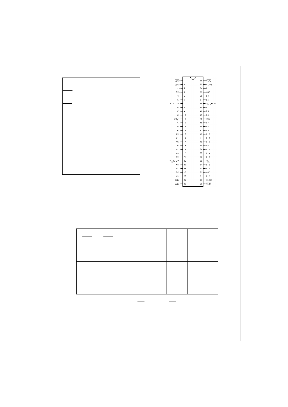
Pin Descriptions Connection Diagram
Functional Description
The GTLP16612 com bines a univers al transceiver f unction with a T TL to GTLP transl ation. The A-P ort and control pins
operate at LVTTL or 5V TTL levels while the B-Port operates at GTLP levels. The transceiver logic includes D-type latch es
and D-type flip-flops to allow data flow in transparent, latched and clock mode.
The functional operation is described in the truth table below.
Truth Table
(Note 1)
Note 1: A-to-B data flo w is sh ow n. B-to-A data flow is similar but uses OEBA, LEBA, CLKBA, and CEBA.
Note 2: Output level before the indicated s t eady-state input conditions were establis hed, provided that CL KAB was high before LE AB went low.
Note 3: Output level before the indicated steady-state input conditions were established.
Pin
Names
Description
OEAB
A-to-B Output Enable (Active LOW)
OEBA
B-to-A Output Enable (Active LOW)
CEAB
A-to-B Clock Enable (Active LOW)
CEBA
B-to-A Clock Enable (Active LOW)
LEAB A-to-B Latch Enable (Transparent HIGH)
LEBA B-to-A Latch Enable (Transparent HIGH)
CLKAB A-to-B Clock Pulse
CLKBA B-to-A Clock Pulse
V
REF
GTLP Input Reference Voltage
A1–A18 A-to-B TTL Data Inputs or
B-to-A 3-STA TE Outputs
B1–B18 B-to-A GTLP Data Inputs or
A-to-B Open Drain Outputs
Inputs Output
B
Mode
CEAB
OEAB LEAB CL KAB A
X H X X X Z Latched
LLLHXB
0
(Note 2) storage
LLLLXB
0
(Note 3) of A data
X L H X L L Transparent
XLHXHH
LLL↑ L L Clocked storage
LLL↑ H H of A data
HLLXXB
0
(Note 3) Clock inhibit
Page 3
3 www.fairchildsemi.com
GTLP16612
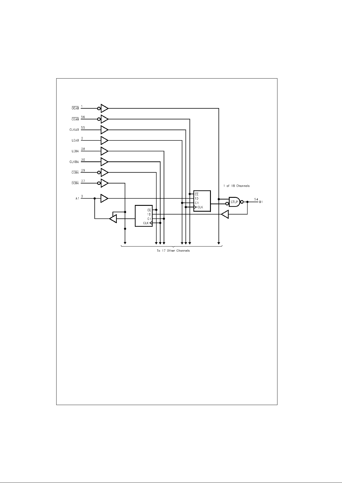
Logic Diagram
Page 4

www.fairchildsemi.com 4
GTLP16612
Absolute Maximum Ratings(Note 4) Recommended Operating
Conditions
(Note 6)
Note 4: The Absolute Maximum Ratings are those values beyond which
the safety of the dev ice cannot be guaranteed. T he device sh ould not be
operated at these limits. The parametric values defined in the Electrical
Characteristic table s are not gua ranteed at the absolute ma ximum rating.
The “Recommend ed O peratin g Cond itions” t able w ill defin e the co ndition s
for actual device operation.
Note 5: I
O
Absolute Maximum Rating must be observed.
Note 6: Unused inputs must be held high or low.
Supply Voltage (VCC, V
CCQ
) −0.5V to +7.0V
DC Input Voltage (V
I
) −0.5V to +7.0V
DC Output Voltage (V
O
)
Outputs 3-STATE −0.5V to +7.0V
Outputs Active (Note 5) −0.5V to V
CC
+ 0.5V
DC Output Sink Current into
A-Port I
OL
64 mA
DC Output Source Current from
A-Port I
OH
−64 mA
DC Output Sink Current
into B-Port in the LOW State,
I
OL
80 mA
DC Input Diode Current (I
IK
)
V
I
< 0V −50 mA
DC Output Diode Current (I
OK
)
V
O
< 0V −50 mA
V
O
> V
CC
+50 mA
Storage Temperat ure (T
STG
) −65°C to +150°C
ESD Perfor mance >2000V
Supply Voltage V
CC
V
CC
3.15V to 3.45V
V
CCQ
4.75V to 5.25V
Bus Termination Voltage (V
TT
) 1.35V to 1.65V
Input Voltage (V
I
)
on A-Port and Control Pins 0.0V to 5.5V
HIGH Level Output Current (I
OH
)
A-Port −32 mA
LOW Level Output Current (I
OL
)
A-Port +32 mA
B-Port +34 mA
Operating Temperature (T
A
) −40°C to +85°C
Page 5

5 www.fairchildsemi.com
GTLP16612
DC Electrical Characteristics
Over Recommended Operating Free-Air Temperature Range, V
REF
= 1.0V (Unless Otherwise Noted).
Note 7: All typicaI values are at VCC = 3.3V, V
CCQ
= 5.0V, and TA = 25°C.
Note 8: For conditions s hown as Min or Max, use the appropriate value s pecified under recom m ended operating conditions.
Note 9: This is the increas e in supply current for eac h input that is at the spec if ied TTL voltage level ra th er than V
CC
or GND.
Symbol Test Conditions Min Typ Max Units
(Note 7)
V
IH
B-Port V
REF
+0.1 V
TT
V
Others 2.0 V
V
IL
B-Port 0.0 V
REF
−0.1 V
Others 0.8
V
REF
1.0 V
V
IK
VCC = 3.15V, II = −18 mA −1.2 V
V
CCQ
= 4.75V
V
OH
A-Port VCC, V
CCQ
= Min to Max (Note 8) IOH = −100 µAV
CC
− 0.2
VCC = 3.15V IOH = −8 mA 2.4 V
V
CCQ
= 4.75V IOH = −32 mA 2.0
V
OL
A-Port VCC, V
CCQ
= Min to Max (Note8) IOL = 100 µA0.2V
VCC = 3.15V IOL = 32 mA 0.5
V
CCQ
= 4.75V
B-Port VCC = 3.15V V
CCQ
= 4.75V IOL = 34 mA 0.65 V
I
I
Control Pins VCC, V
CCQ
= 0 or Max VI = 5.5V or 0V ±10 µA
A-Port VCC = 3.45V VI = 5.5V 20
V
CCQ
= 5.25V VI = V
CC
1 µA
VI = 0 −30
B-Port VCC = 3.45V VI = V
CCQ
5 µA
V
CCQ
= 5.25V VI = 0 −5
I
OFF
A-Port VCC = V
CCQ
= 0V
I
or VO = 0 to 4.5V 100 µA
I
I(hold)
A-Port VCC = 3.15V, VI = 0.8V 75 µA
V
CCQ
= 4.75V VI = 2.0V −20
I
OZH
A-Port VCC = 3.45V, VO = 3.45V 1 µA
B-Port V
CCQ
= 5.25V VO = 1.5V 5
I
OZL
A-Port VCC = 3.45V, VO = 0 −20 µA
B-Port V
CCQ
= 5.25V VO = 0.65V −10
I
CCQ
(V
CCQ
)
A or B VCC = 3.45V, Outputs HIGH 30 40
Ports V
CCQ
= 5.25V, Outputs LOW 30 40 mA
IO = 0,
VI = V
CCQ
or GND Outputs Disabled 30 40
I
CC
(VCC)
A or B VCC = 3.45V, Outputs HIGH 0 1
Ports V
CCQ
= 5.25V, Outputs LOW 0 1 mA
IO = 0,
VI = V
CCQ
or GND Outputs Disabled 0 1
∆I
CC
A-Port and VCC = 3.45V, One Input at 2.7V 0 1 mA
(Note 9) Control Pins V
CCQ
= 5.25V,
A or Control Inputs at
VCC or GND
C
IN
Control Pins VI = V
CCQ
or 0 8
C
I/O
A-Port VI = V
CCQ
or 0 9 pF
C
I/O
B-Port VI = V
CCQ
or 0 6
Page 6

www.fairchildsemi.com 6
GTLP16612
AC Operating Requirements
Over recommended ranges of supply voltage and operating free-air temperature, V
REF
= 1.0V (unless otherwise noted).
AC Electrical Characteristics
Over recommended range of supply voltage and operating free-air temperature, V
REF
= 1.0V (unless otherwise noted).
CL = 30 pF for B-Port and CL = 50 pF for A-Port.
Note 10: All typical v alues are at VCC = 3.3V, V
CCQ
= 5.0V, and TA = 25°C.
Symbol Min Max Unit
f
CLOCK
Max Clock Frequency 175 MHz
t
W
Pulse Duration LEAB or LEBA HIGH 3.0 ns
CLKAB or CLKBA HIGH or LOW 3.2
t
S
Setup Time A before CLKAB↑ 0.5 ns
B before CLKBA↑ 3.1
A before LEAB↓ 1.3
B before LEBA↓ 3.7
CEAB before CLKAB↑ 0.4
CEBA before CLKBA↑ 1.0
t
H
Hold Time A after CLKAB↑ 1.5 ns
B after CLKBA↑ 0.0
A after LEAB↓ 0.5
B after LEBA↓ 0.0
CEAB after CLKAB↑ 1.5
CEBA after CLKBA↑ 1.7
Symbol From To Min Typ Max Unit
(Input) (Output) (Note 10 )
t
PLH
A B 1.0 4.3 6.5 ns
t
PHL
1.0 5.0 8.2
t
PLH
LEAB B 1.8 4.5 6.7 ns
t
PHL
1.5 5.3 8.6
t
PLH
CLKAB B 1.8 4.6 6.7 ns
t
PHL
1.5 5.4 8.7
t
PLH
OEAB B 1.6 4.4 6.2 ns
t
PHL
1.3 6.1 9.8
t
RISE
Transition time, B outputs (20% to 80%) 2.6 ns
t
FALL
Transition time, B outputs (20% to 80%) 2.6
t
PLH
B A 2.0 5.6 8.2 ns
t
PHL
1.4 5.0 7.2
t
PLH
LEBA A 2.1 4.2 6.3 ns
t
PHL
1.9 3.3 5.0
t
PLH
CLKBA A 2.3 4.4 6.8 ns
t
PHL
2.2 3.5 5.2
t
PZH
, t
PZL
OEBA A 1.5 5.0 6.2 ns
t
PHZ
, t
PLZ
1.9 3.9 7.9
Page 7

7 www.fairchildsemi.com
GTLP16612
Test Circuits and Timing Waveforms
Test Circuit for A Outputs
C
L
includes probes and jig capacitance.
Test Circuit for B Outputs
C
L
includes probes and jig capacitance.
For B-Port output s, C
L
= 30 pF is used for
worst case edge rate.
Voltage Waveforms Pulse Duration
(Vm = 1.5V for A-Port and 1.0V for B-Port)
Voltage Waveforms Setup and Hold Times
(Vm = 1.5V for A-Port and 1.0V for B-Port)
Voltage Waveforms Propagation Delay Times
(A-Port to B-P o rt)
Voltage Waveforms Propagation Delay Times
(B-Port to A-P o rt)
All input pulses have the following characteristics: frequency = 10 MHz, tr = tf = 2 ns, ZO = 50Ω. The outputs are measured one at a time with
one transition per measurement.
Voltage Waveforms Enable and Disable Times (A-Port)
Waveform 1 is for an ou t put w ith internal conditions such that the output is low exc ept when disabled by t he output control. Waveform 2 is for an output w ith
internal conditions suc h that the output is high except when disabled by the ou t put c ont rol. All input pulses have the following characteristics: frequency = 10
MHz, tr = tf = 2 ns, ZO = 50Ω. The outputs are me as ured one at a time with one transition per meas urement.
Page 8

www.fairchildsemi.com 8
GTLP16612
Physical Dimensions inches (millimeters) unless otherwise noted
56-Lead Shrink Small Outline Package, JEDEC MO-118 0.300” Wide
Package Number MS56A
Page 9

Fairchild does not assume any responsibility for use of any circuitry described, no circuit patent licenses are implied and Fairchild reserves the right at any time without notice to change said circuitry and specifications.
GTLP16612 CMOS 18-Bit TTL/GTLP Universal Bus Transceiver
LIFE SUPPORT POLICY
FAIRCHILD’S PRODUCTS ARE NOT AUTHORIZED FOR USE AS CRITICAL COMPONENTS IN LIFE SUPPORT
DEVICES OR SYSTEMS WITHOUT THE EXPRESS WRITTEN APPROVAL OF THE PRESIDENT OF FAIRCHILD
SEMICONDUCTOR CORPORATION. As used herein:
1. Life support devices or system s are de vices o r syste ms
which, (a) are intended for surgical implant into the
body, or (b) support or sustain life, and (c) whose failure
to perform when properly used in accordance with
instructions for use provide d in the lab el ing , can be re asonably expected to result in a significant in jury to the
user.
2. A critical component in any component of a life support
device or system whose failure to perform can be r easonably expected to cau se th e f ail ur e o f the life sup por t
device or system, or to affect its safety or effectiveness.
www.fairchildsemi.com
Physical Dimensions inches (millimeters) unless otherwise noted
56-Lead Thin Shrink Small Outline Package, JEDEC MO-153, 6.1mm Wide
Package Number MTD56
 Loading...