

Page 1
GTLP10B320
10-Bit LVTTL/GTLP Transceiver
with Split LVTTL Port and Feedback Path
GTLP10B320 10-Bit LVTTL/GTLP Transceiver with Split LVTTL Port and Feedback Path
May 2001
Revised May 2001
General Description
The GTLP10B320 is a 10-bit Universal bus driver and
receiver, with separate LVTTL inputs and outputs and a
feedback path for diagnostics, that provides LVTTL to
GTLP signal level t ranslatio n. H igh spe ed bac kplan e operation is a direct result of GTLP’s reduced output swing
(
<1V), reduced input thresh old le vels a nd outp ut edg e rate
control. The edge rate c ontrol mi nimizes b us settl ing time.
GTLP is a Fairchild Semiconductor derivative of the
Gunning Transistor logic (GTL) JEDEC stan dard JESD8-3.
Fairchild’s GTLP has intern al edge -rate cont rol and i s process, voltage and temperature (PVT) compensated. Its
function is similar to BTL and GT L but with different o utput
levels and receiver threshold. GTLP out put l ow level i s typically less than 0.5V, the output level high is 1.5V and the
receiver threshold is 1.0V.
Features
■ Bidirectional interface between GTLP and LVTTL logic
levels
■ Variable edge rate control pin to select desired edge rate
on GTLP port (V
pin provides extern al supply re ference volta ge for
■ V
REF
receiver threshold adjustibility
■ Split LVTTL inputs and outputs
■ Special PVT compensation circui try to provide consis-
tent performance over var iatio ns of pr ocess, supply voltage and temperature
■ A feedback path for control and diagnostics monitoring
■ TTL compatible driver and control inputs
■ Designed using Fairchild advanced BiCMOS technology
■ Bushold data inputs on A port to e liminate the need for
external pull-up resistors for unused inputs
■ Power up/down and power off high impedance for live
insertion
■ Open drain on GTLP to support wired-or connection
■ Flow through pinout optimizes PCB layout
■ A Port source/sink
■ B Port sink
+50mA
)
ERC
−24mA/+24mA
Ordering Code:
Order Number Package Number Package Description
GTLP10B320MTD MTD56 56-Lead Thin Shrink Small Outline Package (TSSOP), JEDEC MO-153, 6.1mm Wide
Device is also available in Tape and Reel. Specify by append ing the suffix letter “X” to the ordering code.
© 2001 Fairchild Semiconductor Corporation DS500483 www.fairchildsemi.com
Page 2
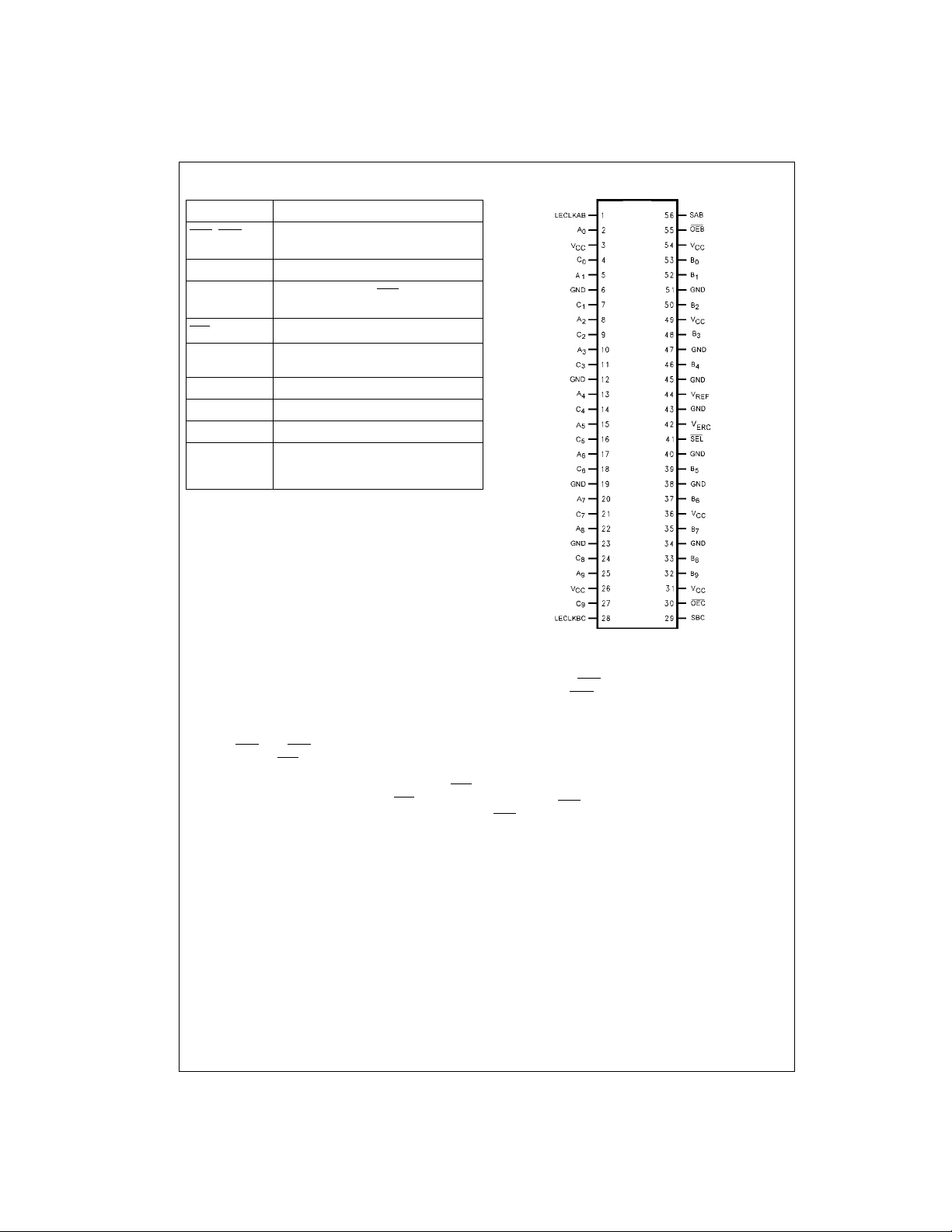
Pin Descriptions Connection Diagram
Pin Names Description
, OEC B Port, C Port Output Enable
OEB
GTLP10B320
, GND, V
V
CC
LECLKAB,
LECLKBC
SEL
SAB, SBC Selects Register or Latch/Transparent
B
0-B9
A
0-A9
C
0-C9
V
ERC
respectively (Active LOW)
Device Supplies
REF
A-to-B, B-to-C Latch CLK
(Transparent Active HIGH)
Selects Internal Feedback Path
Path for A-to-B and B-to-C respectively
B Port GTLP I/O
A Port LV TTL Inputs
C Port LVTTL Outputs
Edge Rate Control Pin
= Slow Edge Rate)
(GND
= Fast Edge Rate)
(V
CC
respectively
Functional Description
The GTLP10B320 is a 10-bit Univ ersal drive r and receive r
containing D-Type flip-flop, latch, and transparent modes of
operation for the data paths. In addition there is an internal
feedback pat h tha t ca n be used for di agno st ic mon it orin g or
caching schemes. Data flow i n each dir ection is controlled
by the clock signals (LECLKAB and LECLKBC) an d o utp ut
enables (OEB
controlled by t he SEL
Port A to Port C wit hout requiring data to be ou tput to the
backplane. Th e in t er nal f ee dba c k pat h i s s ele c t ed wi th S EL
LOW and the B Port pin is selected w ith SEL HIGH. The
data paths can also be configured for latch/transparent or
register mode for each direction with the SAB and SBC
www.fairchildsemi.com 2
and OEC). The internal feedback path is
pin and allows data transfer from
pins. Data polarity is non-inverting wi th the GTLP outputs
enabled via the OEB
enabled via the OEC
For A-to-B data flow the device is configured in to a latch/
transparent or register mode by pin SAB. If SAB is LOW
then the register mode is sel e cted and th e de vice op era tes
on the LOW-to-HIGH transition of LECLKAB. If SAB is
HIGH then the latch/transpa rent configuration is selected
and a HIGH-to-LOW transit ion of LECLKAB sto res data in
the latch. If LECLKAB is HIGH the device is in transparent
mode. When OEB
OEB
is HIGH the outputs are high impedance.
pin and the LVTTL outputs being
pin.
is LOW the outputs are active and when
Page 3
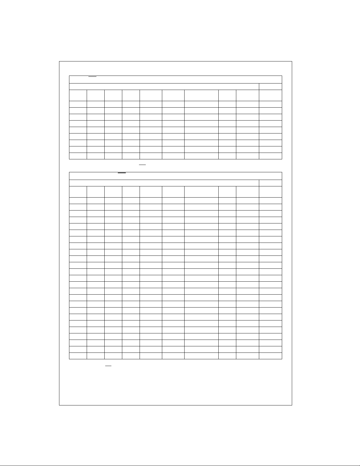
Functional Tables
I/O Path: SEL = 1 (External Feedback Path) (Note 2)
Inputs Outputs
OEB OEC SAB SBC LECLKAB LECLKBC Mode
(AB)
010X ↑ XRegisterLX L
010X
↑ XRegisterHX H
010X L X Register L XB
010X L X Register H XB
011X
↓ X Latch L X L
011X H X Buffer L X L
011X
↓ X Latch H X H
011X H X Buffer H X H
1 1 X X X X High Impedance X X Z
Note 1: Output level before the indicated steady stat e input conditions were es t ablished.
Note 2: The data flow of B-to-C is similar except that OEC
Internal Feedback Path: SEL
= 0 (Internal Feedback Path) (Note 3)
, SBC and LECLK BC are used.
Inputs Outputs
OEB OEC SAB SBC LECLKAB LECLKBC Mode
(AB/BC)
0000 ↑↑Register/Register L L L
0000
0000 L
0000
0000
↑↑Register/Register H H H
↑ Register/Register X B
↑ L Register/Register L L B
↑ L Register/Register H H B
0000 L LRegister/RegisterXB
0001
0001
0001
0001
0001 L
↑↓Register/Latch L L L
↑ H Register/Buffer L L L
↑↓Register/Latch H H H
↑ H Register/Buffer H H H
↓ Register/Latch X B
0001 L HRegister/BufferXB
0001 L LRegister/LatchXB
0010
0010
0010
0010
0010 H
0010 H
↓↑Latch/Register L L L
↓↑Latch/Register H H H
↓ L Latch/Register L L B
↓ L Latch/Register H H B
↑ Buffer/Register L L L
↑ Buffer/Register H H H
0010 L LLatch/RegisterXB
0011
0011
↓↓Latch/Latch L L L
↓↓Latch/Latch H H H
0011 H HBuffer/BufferL L L
0011 H HBuffer/BufferH H H
1 1 X X X X High Impedance X Z Z
A
n
A
n
(Note 4) B0 (Note 4)
0
(Note 4) B0 (Note 4)
0
(Note 4) B0 (Note 4)
0
(Note 4) B0 (Note 4)
0
(Note 4) B0 (Note 4)
0
(Note 4) B0 (Note 4)
0
C
n
B
n
B
n
(Note 1)
0
(Note 1)
0
C
n
(Note 4)
0
(Note 4)
0
(Note 4)
0
(Note 4)
0
GTLP10B320
Note 3: Function identical for SEL
Note 4: Output level before the indicated steady stat e input conditions were es t ablished.
= 1 if timing requirem ents for propagatio n delay to output and set -up to LECLKBC are m et at B Port.
3 www.fairchildsemi.com
Page 4
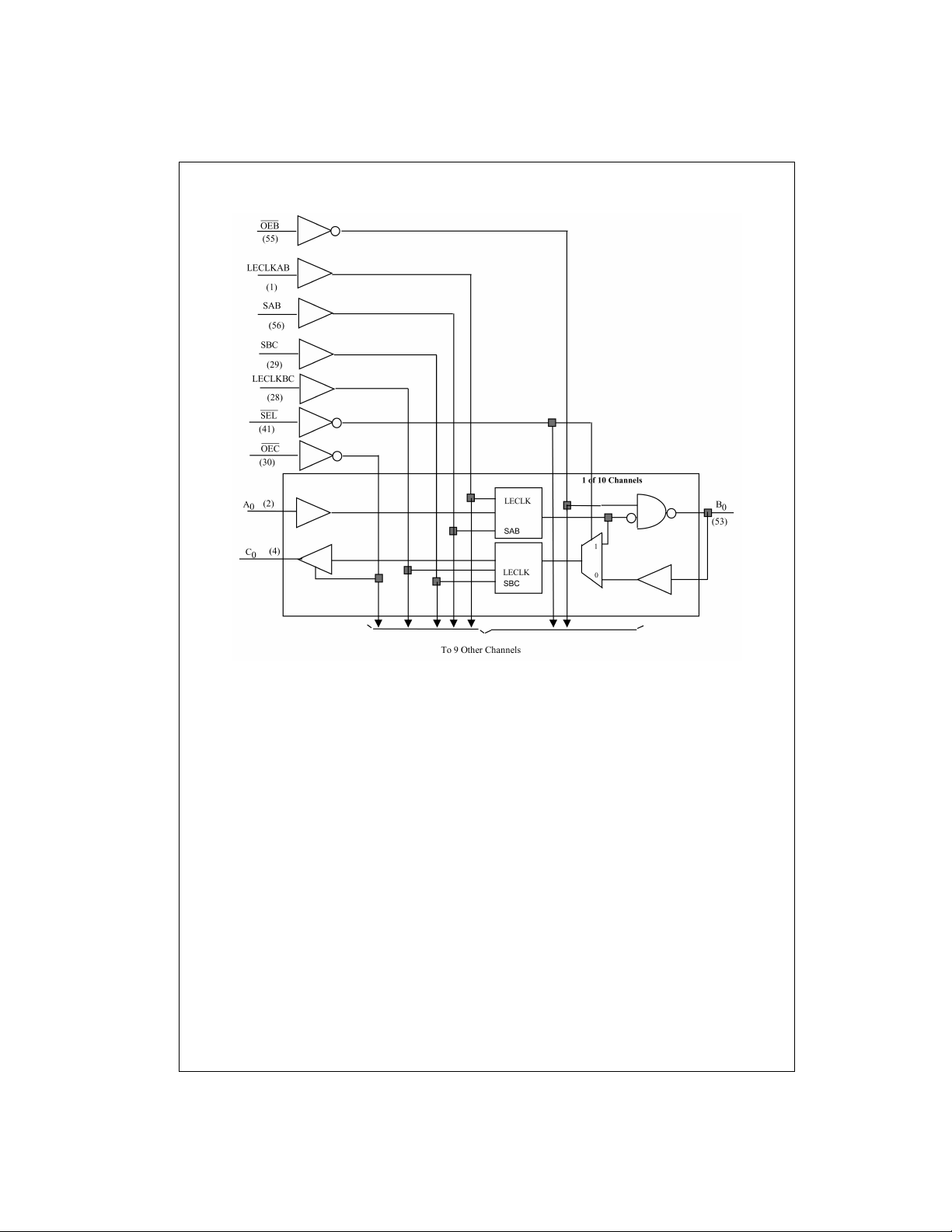
Logic Diagram
GTLP10B320
www.fairchildsemi.com 4
Page 5

Absolute Maximum Ratings(Note 5) Recommended Operating
Supply Voltage (VCC) −0.5V to +4.6V
DC Input Voltage (V
DC Output Voltage (V
Outputs 3-STATE
Outputs Active (Note 6)
) −0.5V to +4.6V
I
)
O
−0.5V to +4.6V
−0.5V to +4.6V
DC Output Sink Current into
C Port I
OL
48 mA
DC Output Source Current from
C Port I
OH
−48 mA
DC Output Sink Current into
B Port in the LOW State, I
DC Input Diode Current (I
< 0V −50 mA
V
I
DC Output Diode Current (I
V
< 0V −50 mA
O
OL
)
IK
)
OK
ESD Rating
Storage Temperature (T
) −65°C to +150°C
STG
100 mA
>2000V
Conditions
Supply Voltage V
Bus Termination Voltage (V
GTLP 1.47V to 1.53V
V
REF
Input Voltage (V
on A Port and Control Pins 0.0V to V
HIGH Level Output Current (IOH)
C Port
LOW Level Output Current (I
C Port
B Port
Operating Temperature (T
Note 5: Absolute Maximum Ratings are those values beyond which the
safety of the device can not be gu arant eed. The de vice sh ould no t be operated at these limits. The parametric values defined in the “Electrical Characteristics” table are not guarant eed at the ab solute max imum ratin g. The
“Recommended Operating Con ditions” table will define the conditions for
actual device opera tion.
Absolute Maximum Rating must be observed.
Note 6: I
O
CC
)
I
)
TT
)
OL
) −40°C to +85°C
A
DC Electrical Characteristics
Over Recommended Operating Free-Air Temperature Range, V
Symbol Test Conditio ns
V
IH
V
IL
V
REF
V
TT
V
IK
V
OH
V
OL
I
I
I
OFF
B Port V
Others 2.0
B Port 0.0 V
Others 0.8
B Port 0.7 1.0 1.3 V
B Port V
C Port VCC = Min to Max (Note 8) IOH = −100 µAV
C Port VCC = Min to Max (Note 8) IOL = 100 µA0.2
B Port VCC = 3.15V IOL = 40 mA 0.4
Control Pins VCC = 3.45V VI = 3.45V 10
and A Port VI = 0V −10
B Port VCC = 3.45V VI = V
A or C Ports, VCC = 0V
Control Pins
B Port VCC = 0V
VCC = 3.15V II = −18 mA −1.2 V
= 3.15V IOH = −8 mA 2.4
CC
= 3.15V IOL = 8 mA 0.4
CC
= 1.0V (unless otherwise noted).
REF
IOH = -24mA 2.2
IOL = 24 mA 0.5
IOL = 50 mA 0.5
TT
VI = 0 −5
or VO = 0 to 3.45V 30 µA
I
or VO = 0 to 1.5V 30 µA
I
Min Typ Max Units
+ 0.05 V
REF
+ 50 mV 1.5 V
REF
–0.2
CC
(Note 7)
3.15V to 3.45V
0.98V to 1.02V
TT
− 0.05
REF
CC
5
GTLP10B320
CC
−24 mA
+24 mA
+50 mA
V
V
V
VV
VV
V
µA
µA
I
I (HOLD)
I
OZH
I
OZL
I
PU/PD
A Port VCC = 3.15V VI = 0.8V 75
VI = 2.0V −75
C Port VCC = 3.45V VO = 3.45V 10
B Port VO = 1.5V 5
C Port VCC = 3.45V VO = 0V −10
B Port VO = 0.55V −5
All Ports VCC = 0 to 1.5V VI = 0 to 3.45V 30 µA
5 www.fairchildsemi.com
µA
µA
µA
Page 6

DC Electrical Characteristics (Continued)
Symbol Test Conditions
I
A or B Ports VCC = 3.45V Outputs HIGH 27 45
CC
Min Typ Max Units
(Note 7)
GTLP10B320
= VCC/VTT or GND Outputs Disabled 27 45
V
∆I
CC
A Port and VCC = 3.45V, One Input at V
I
CC
(Note 9) Control Pins A or Control Inputs at VCC or GND −0.6V
C
i
Control Pins VI = VCC or 0 4.5
and A Port
C Port V
B Port V
Note 7: All typical values are at VCC = 3.3V and TA = 25°C.
Note 8: For conditions shown as Min, use the appropri at e v alue specified under recommended operating conditions.
Note 9: This is the increase in supply current for each input that is at the specif ied TTL voltage level rather than V
Note: GTLP V
addition, V
within the boundaries of the DC Absolu te M ax im um Ratings. Simil arly, V
and VTT are specified to 2 % tolerance sinc e s ignal integrity and noise margin ca n be significantly degraded if these supplies are noisy. In
REF
and R
TT
can be adjusted bey ond the recom mende d operating to accomm odate bac kplane impe dances o ther than 50 Ω, but must remain
TERM
= VCC or 0 6
I
= VCC or 0 9
I
or GND.
CC
can be adjusted to optimize noise margin.
REF
AC Operating Requirements
Over recommended ranges of supply voltage and operating free-air temperature, V
Symbol Test Conditions Min Max Unit
f
MAX
t
WIDTH
t
SET
Maximum Clock Frequency 150 MHz
Pulse Duration LECLKAB, LECLKBC HIGH or LOW 3.0 ns
Setup Time SAB = 0 A before LECLKAB↑ 2.1
SBC = 0 B before LECLKBC↑ 2.6
SAB = 1, SEL = 1, SBC = 0 A before LECLKBC↑ 6.8
SAB = 1, SEL = 0, SBC = 0 A before LECLKBC↑ 3.0
SAB = 1 A before LECLKAB↓ 1.7
SBC = 1 B before LECLKBC↓ 2.2
SAB = 1, SEL = 1, SBC = 1 A before LECLKBC↓ 6.4
SAB = 1, SEL = 0, SBC = 1 A before LECLKBC↓ 2.8
t
HOLD
Hold Time SAB = 0 A after LECLKAB↑ 2.0
SBC = 0 B after LECLKBC↑ 1.6
SAB = 1, SEL
SAB = 1, SEL
= 1, SBC = 0 A after LECLKBC↑−1.4
= 0, SBC = 0 A after LECLKBC↑ 1.4
SAB = 1 A after LECLKAB↓ 2.5
SBC = 1 B after LECLKBC↓ 2.1
SAB = 1, SEL
= 1, SBC = 1 A after LECLKBC↓−1.0
SAB = 1, SEL = 0, SBC = 1 A after LECLKBC↓ 1.6
= 1.0V (unless otherwise noted).
REF
mAor C Port IO = 0 Outputs LOW 27 45
2mA
pF
ns
ns
www.fairchildsemi.com 6
Page 7

AC Electrical Characteristics
Over recommended range of supply voltage and operating free air temperature, V
V
= GND. CL = 30 pF for B Port and CL = 50 pF for C Port.
ERC
Symbol
t
PLH
t
PHL
t
PLH
t
PHL
t
PLH
t
PHL
t
PLH
t
PHL
t
PLH
t
PHL
t
PLH
t
PHL
t
PLH
t
PHL
t
PLH
t
PHL
t
PLH
t
PHL
t
PLH
t
PHL
t
PLH
t
PHL
t
PLH
t
PHL
t
RISE
t
FALL
t
RISE
t
FALL
t
PLH
t
PHL
t
, t
PZH
PZL
t
, t
PHZ
PLZ
t
, t
PZH
PZL
t
, t
PHZ
PLZ
Note 10: All typical valu es are at VCC = 3.3V, and TA = 25°C.
From To Min Typ Max Unit
(Input) (Output) (Note 10)
A
n
LECLKAB B
LECLKAB B
B
n
LECLKBC C
LECLKBC C
A
n
B
n
n
n
C
n
n
n
C
n
SEL = 1, SAB = 1, SBC = 1 2.4 5.1 8.0
A
n
C
n
SEL = 0, SAB = 1, SBC = 1 1.9 3.4 5.8
LECLKAB C
n
SEL = 1, SAB = 1, SBC = 1 3.0 5.5 8.6
LECLKAB C
n
SEL = 0, SAB = 1, SBC = 1 1.9 3.6 6.3
LECLKAB C
n
SEL = 1, SAB = 0, SBC = 1 2.9 5.5 8.6
LECLKAB C
n
SEL = 0, SAB = 0, SBC = 1 2.0 3.7 6.5
Transition Time, B Outputs (20% to 80%) 2.2
Transition Time, B Outputs (80% to 20%) 1.8
Transition Time, C Outputs (10% to 90%) 1.5
Transition Time, C Outputs (90% to 10%) 1.6
SEL C
OEB B
OEC C
n
n
n
= 1.0V (unless otherwise noted).
REF
2.0 4.2 7.5
SAB = 1 1.1 2.7 4.9
2.2 4.5 6.7
SAB = 1 1.3 3.0 5.6
2.5 4.8 7.1
SAB = 0 1.4 3.1 5.7
1.4 2.6 4.4
SBC = 1 1.6 2.9 5 .0
1.2 2.5 4.5
SBC = 1 1.5 2.9 5 .0
1.3 2.6 4.6
SBC = 0 1.5 2.9 5 .0
3.3 6.1 10.3
1.5 3.0 5.4
2.6 6.5 9.5
1.8 3.4 6.0
2.7 6.8 10.0
1.8 3.5 6.3
1.2 2.8 4.9
1.5 2.8 5.3
1.1 2.8 5.2
2.0 4.3 8.9
1.2 2.9 5.3
1.4 2.8 4.9
GTLP10B320
ns
ns
ns
ns
ns
ns
ns
ns
ns
ns
ns
ns
ns
ns
ns
ns
7 www.fairchildsemi.com
Page 8

AC Electrical Characteristics
Over recommended range of supply voltage and operating free air temperature, V
V
= GND. CL = 10 pF for B Port and CL = 10 pF for C Port.
ERC
Symbol
t
PLH
GTLP10B320
t
PHL
t
PLH
t
PHL
t
PLH
t
PHL
t
PLH
t
PHL
t
PLH
t
PHL
t
PLH
t
PHL
t
PLH
t
PHL
t
PLH
t
PHL
t
PLH
t
PHL
t
PLH
t
PHL
t
PLH
t
PHL
t
PLH
t
PHL
t
RISE
t
FALL
t
RISE
t
FALL
t
PLH
t
PHL
t
, t
PZH
PZL
t
, t
PHZ
PLZ
t
, t
PZH
PZL
t
, t
PHZ
PLZ
Note 11: All typical values are at VCC = 3.3V, and TA = 25°C.
From To Min Typ Max Unit
(Input) (Output) (Note 11)
A
n
LECLKAB B
LECLKAB B
B
n
LECLKBC C
LECLKBC C
A
n
SEL = 1, SAB = 1, SBC = 1 1.0 4.1 7.1
A
n
SEL = 0, SAB = 1, SBC = 1 0.8 2.6 5.2
LECLKAB C
SEL = 1, SAB = 1, SBC = 1 1.4 4.3 7.6
LECLKAB C
SEL = 0, SAB = 1, SBC = 1 0.9 2.8 5.6
LECLKAB C
SEL = 1, SAB = 0, SBC = 1 1.3 4.3 7.6
LECLKAB C
SEL = 0, SAB = 0, SBC = 1 0.9 2.9 5.8
Transition Time, B Outputs (20% to 80%) 2.0
Transition Time, B Outputs (80% to 20%) 1.8
Transition Time, C Outputs (10% to 90%) 0.6
Transition Time, C Outputs (90% to 10%) 0.7
SEL C
OEB B
OEC C
= 1.0V (unless otherwise noted).
REF
B
n
1.6 3.9 7.2
SAB = 1 0.7 2.4 4.7
n
1.7 4.1 6.3
SAB = 1 0.9 2.7 5.4
n
2.0 4.4 6.7
SAB = 0 1.0 2.7 5.4
C
n
0.4 1.8 3.7
SBC = 1 0.6 2.2 4.3
n
0.2 1.8 3.9
SBC = 1 0.4 2.0 4.3
n
0.3 1.8 4.0
SBC = 0 0.4 2.1 4.3
C
n
C
n
n
n
n
n
n
2.1 5.1 9.3
0.5 2.3 4.8
1.1 5.3 8.5
0.8 2.6 5.4
1.2 5.6 9.0
0.9 2.8 5.6
0.3 1.7 4.3
0.4 2.3 4.6
n
0.8 2.5 4.8
1.6 4.0 8.5
n
0.6 2.0 4.0
0.6 1.9 3.7
ns
ns
ns
ns
ns
ns
ns
ns
ns
ns
ns
ns
ns
ns
ns
ns
www.fairchildsemi.com 8
Page 9

AC Electrical Characteristics
Over recommended range of supply voltage and operating free air temperature, V
V
= VCC. CL = 30 pF for B Port and CL = 50 pF for C Port.
ERC
Symbol
t
PLH
t
PHL
t
PLH
t
PHL
t
PLH
t
PHL
t
PLH
t
PHL
t
PLH
t
PHL
t
PLH
t
PHL
t
RISE
t
FALL
t
, t
PZH
PZL
t
, t
PHZ
PLZ
Note 12: All typical valu es are at VCC = 3.3V, and TA = 25°C.
From To Min Typ Max Unit
(Input) (Output) (Note 12)
A
n
LECLKAB B
LECLKAB B
A
n
B
n
n
n
C
n
SEL = 1, SAB = 1, SBC = 1 2.0 4.7 7.5
LECLKAB C
n
SEL = 1, SAB = 1, SBC = 1 2.2 5.1 8.1
LECLKAB C
n
SEL = 1, SAB = 0, SBC = 1 2.3 5.1 8.2
Transition Time, B Outputs (20% to 80%) 1.8
Transition Time, B Outputs (80% to 20%) 1.4
OEB B
n
AC Electrical Characteristics
Over recommended range of supply voltage and operating free air temperature, V
V
= VCC. CL = 10 pF for B Port and CL = 10 pF for C Port.
ERC
Symbol
t
PLH
t
PHL
t
PLH
t
PHL
t
PLH
t
PHL
t
PLH
t
PHL
t
PLH
t
PHL
t
PLH
t
PHL
t
RISE
t
FALL
t
, t
PZH
PZL
t
, t
PHZ
PLZ
Note 13: All typical valu es are at VCC = 3.3V, and TA = 25°C.
From To Min Typ Max Unit
(Input) (Output) (Note 13)
A
n
LECLKAB B
LECLKAB B
A
n
B
n
n
n
C
n
SEL = 1, SAB = 1, SBC = 1 0.6 3.7 6.6
LECLKAB C
n
SEL = 1, SAB = 1, SBC = 1 0.7 3.9 7.2
LECLKAB C
n
SEL = 1, SAB = 0, SBC = 1 0.8 3.9 7.2
Transition Time, B Outputs (20% to 80%) 1.4
Transition Time, B Outputs (80% to 20%) 1.2
OEB B
n
= 1.0V (unless otherwise noted).
REF
1.2 3.3 7.3
SAB = 1 0.8 2.3 4.5
1.4 3.7 6.0
SAB = 1 1.0 2.6 5.1
1.6 3.9 6.3
SAB = 0 1.1 2.7 5.2
1.6 5.3 8.1
1.7 5.7 8.8
1.8 5.9 9.1
0.5 2.4 4.7
1.7 3.4 5.9
= 1.0V (unless otherwise noted).
REF
0.8 3.0 7.0
SAB = 1 0.5 2.1 4.3
0.6 3.2 5.7
SAB = 1 0.6 2.3 4.8
0.8 3.5 6.0
SAB = 0 0.7 2.4 4.9
0.2 4.2 8.1
0.2 4.5 7.7
0.3 4.8 8.0
0.2 2.1 4.4
1.3 3.0 5.5
GTLP10B320
ns
ns
ns
ns
ns
ns
ns
ns
ns
ns
ns
ns
ns
ns
ns
ns
9 www.fairchildsemi.com
Page 10

AC Extended Electrical Characteristics
Over recommended ranges of supply voltage and operating free air temperature V
C
= 30 pF for B Port and CL = 50 pF for C Port.
L
t
OSLH
t
OSHL
GTLP10B320
t
PVHL
t
OSLH
t
OSHL
t
PVHL
t
OSLH
t
OSHL
t
PVHL
t
OSLH
t
OSHL
t
(Note 14) B C
OST
t
(Note 15) B C
PV
t
OSLH
t
OSHL
t
(Note 14) LECLKBC C
OST
Symbol Path From To Mode Max Unit
(Note 14) A B
(Note 14) 0.4
(Note 15)(Note 16) A B
(Note 14) LECLKAB B
(Note 14) 0.4
(Note 15)(Note 16) LECLKAB B
(Note 14) LECLKAB B
(Note 14) 0.4
(Note 14)(Note 15) LECLKAB B
(Note 14) B C
(Note 14) 0.4
(Note 14) LECLKBC C
(Note 14) 0.4
tPV (Note 15) LECLKBC C
t
(Note 14) LECLKBC C
OSLH
t
(Note 14) 0.4
OSHL
t
(Note 14) LECLKBC C
OST
tPV (Note 15) LECLKBC C
t
(Note 14) SEL C
OSLH
t
(Note 14) 0.4
OSHL
t
(Note 14) SEL C
OST
t
(Note 15) SEL C
PV
Note 14: t
within the same packaged de vi ce . T he specifications are given for specific worst cas e V
direction either HIGH-to-LOW (t
statistical proces s distrib ution. Actual ske w valu es betwe en the G TLP outp uts could vary on the back plane du e to the loading an d impedance seen by the
device.
Note 15: t
The parameter is specified for a specific worst case V
skew values between the GTLP outputs could vary on the backplane due to the loading and impedance seen by the device.
Note 16: Due to the open drain structure on GTLP outputs t
V
and RT values on the backplane.
TT
and t
OSHL/tOSLH
- Part to part skew is defined as the absolute value of the difference between the actual propagation delay for all outputs from device to dev ic e.
PV
- Output to out put skew is defined as the absolute value of t he difference bet w ee n the actual propagat ion delay for all ou t puts
OST
) or LOW-to-HIGH (t
OSHL
) or in opposite direct ions both HL and LH (t
OSLH
and temperature. This parameter is guaranteed by design and statistical process distribution. Actual
CC
and t
OST
in the A-to-B direction are not specified. Skew on these paths is dependent on the
PV(LH)
= 1.0V (unless otherwise noted).
REF
n
n
n
n
n
n
n
n
n
n
n
n
n
n
n
n
n
n
B
(n+1)
B
(n+1)
B
(n+1)
B
(n+1)
B
(n+1)
B
(n+1)
C
(n+1)
C
(n+1)
C
(n+1)
C
(n+1)
C
(n+1)
C
(n+1)
C
(n+1)
C
(n+1)
C
(n+1)
C
(n+1)
C
(n+1)
C
(n+1)
and temperature and apply to any outputs switc hing in the same
CC
SAB = 1 0.5
SAB = 1 2.0 ns
SAB = 1 0.5
SAB = 1 2.0 ns
SAB = 0 0.5
SAB = 0 2.0 ns
SBC = 1 0.4
SBC = 1 1.0 ns
SBC = 1 1.5 ns
SBC = 1 0.4
SBC = 1 1.0 ns
SBC = 1 1.5 ns
SBC = 0 0.4
SBC = 0 1.0 ns
SBC = 0 1.5 ns
0.4
1.0 ns
1.2 ns
). This parameter is guaranteed by design and
OST
ns
ns
ns
ns
ns
ns
ns
www.fairchildsemi.com 10
Page 11

Test Circuits and Timing Waveforms
GTLP10B320
Tes t Circuit for A Outputs
Test Circuit for B Outputs
Test S
t
PLH/tPHL
t
PLZ/tPZL
t
Note A: CL includes probes and Jig capacitance.
PHZ/tPZH
Open
6V
GND
Note B: For B Port, CL = 30 pF or 10 pF.
Voltage Waveform - Propagation Delay Times Voltage Waveform - Setup and Hold Times
Voltage Waveform - Pulse Width Voltage Waveform - Enable and Disable times
Input and Measure Conditions
A or LVTTL
V
inHIGH
V
inLOW
V
M
V
X
V
All input pulses have the following characteristics: Frequency = 10MHz, t
The outputs are me as ured one at a time with one transition per me as urement.
Y
VOL + 0.3V N/A
VOH − 0.3V N/A
RISE
Output Waveform 1 is for an output with internal conditions such that the
output is LOW except when disabled by th e c ontrol output.
Output Waveform 2 is for an output with internal conditions such that the
output is HIGH except when disabled by t he c ontrol output.
Pins
V
CC
B or GTLP
Pins
1.5
0.0 0.0
VCC/2 1.0
= t
= 2 ns (10% to 90%), ZO = 50Ω
FALL
11 www.fairchildsemi.com
Page 12

Physical Dimensions inches (millimeters) unless otherwise noted
56-Lead Thin Shrink Small Outline Package (TSSOP), JEDEC MO-153, 6.1mm Wide
Package Number MTD56
GTLP10B320 10-Bit LVTTL/GTLP Transceiver with Split LVTTL Port and Feedback Path
Fairchild does not assume any responsibility for use of any circuitr y described, no circuit patent licenses are implied a nd
Fairchild reserves the right at any time without notice to change said circuitry and specifications.
LIFE SUPPORT POLICY
FAIRCHILD’S PRODUCTS ARE NOT AUTHORIZED FOR USE AS CRITICAL COMPONENTS IN LIFE SUPPORT
DEVICES OR SYSTEMS WITHOUT THE EXPRESS WRITTEN APPROVAL OF THE PRESIDENT OF FAIRCHILD
SEMICONDUCTOR CORPORATION. As used herein:
1. Life support devices or systems are device s or syste ms
which, (a) are intended for surgical implant into the
body, or (b) support or sustain life, and (c) whose failure
to perform when properly used in accordance with
instructions for use provided in the labeling, can be reasonably expected to result in a significant inju ry to the
user.
www.fairchildsemi.com 12
2. A critical component in any compon ent of a life supp ort
device or system whose failu re to perform can be reasonably expected to cause the failure of the li fe su pp ort
device or system, or to affect its safety or effectiveness.
www.fairchildsemi.com
 Loading...