

Page 1
INTEGRATED CIRCUITS
GTL2004
Quad GTL/GTL+ to LVTTL/TTL
bidirectional latched translator
Product specification
Supersedes data of 1999 May 15
1999 Jul 19
Page 2
Philips Semiconductors Product specification
SYMBOL
PARAMETER
UNIT
Quad GTL/GTL+ to LVTTL/TTL
bidirectional latched translator
FEA TURES
•Operates as a quad GTL/GTL
LVTTL/TTL to GTL/GTL+ driver
•Quad bidirectional bus interface
•Separate latch enable for each bit
•Live insertion/extraction permitted
•B outputs include 30Ω series resistance
•Latch-up protection exceeds 500mA per JEDEC Std 17
•ESD protection exceeds 2000V per JEDEC Std
DESCRIPTION
The GTL2004 is a quad translating transceiver designed for 3.3V
system interface with a GTL/GTL
The direction pin allows the part to function as either a GTL to TTL
sampling receiver or as a TTL to GTL interface. Separate latch
enables allow sampling and holding of data from the GTL bus.
+
sampling receiver or as a
+
bus.
GTL2004
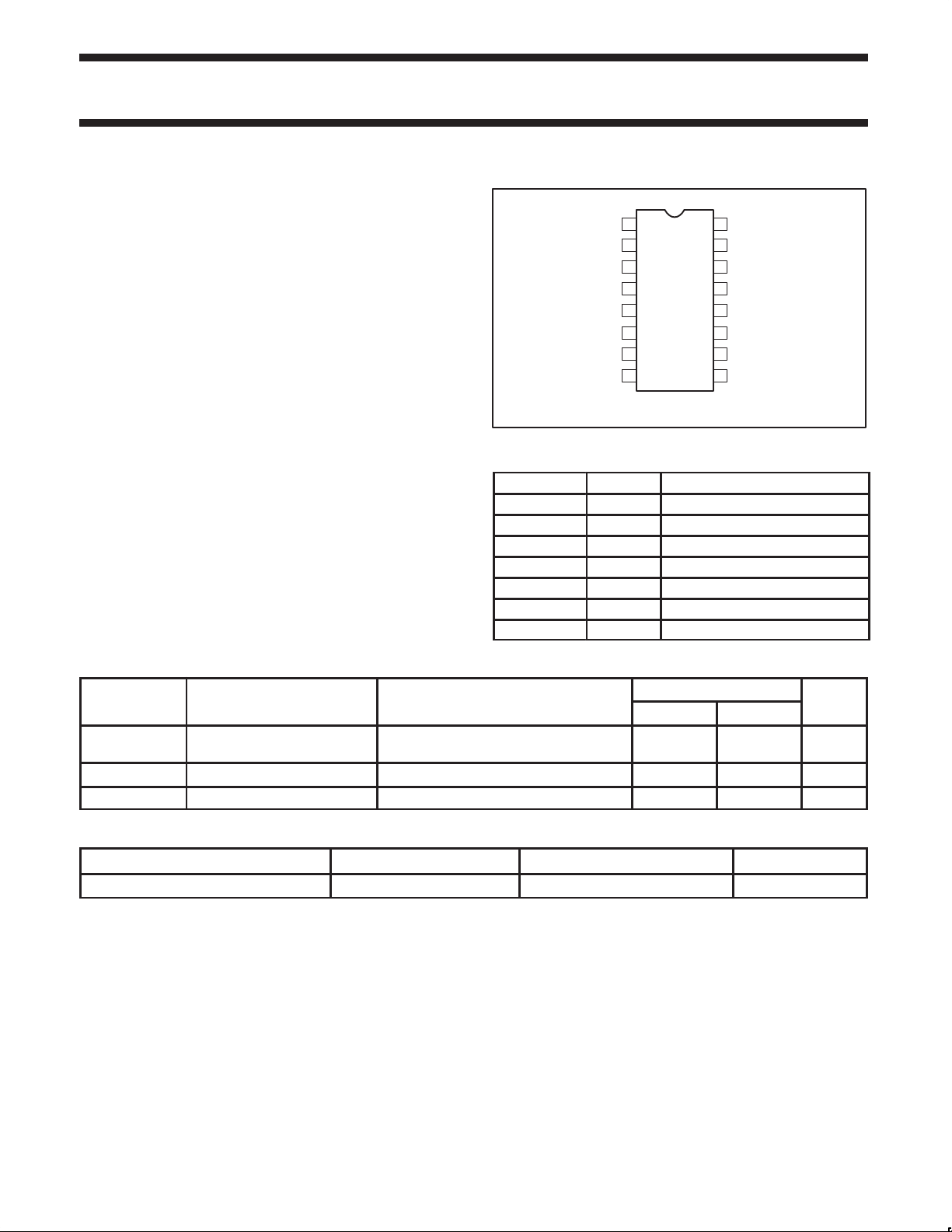
PIN CONFIGURATION
1A0
2
LE0
A1
3
4
LE1
A2
5
LE2
6
A3
7
GND
8
PIN DESCRIPTION
PIN NUMBER SYMBOL NAME AND FUNCTION
15 DIR Direction control input
1, 3, 5, 7 A0 – A3 Data inputs/outputs (A side, GTL)
11, 12, 13, 14 B0 – B3 Data inputs/outputs (B side, TTL)
2, 4, 6, 9 LE0 – LE3 Latch enables
10 GTLREF GTL reference voltage
8 GND Ground (0V)
16 V
CC
V
16
CC
DIR
15
14
B0
B1
13
B2
12
11
B3
GTLREF
10
9
LE3
SW00318
Positive supply voltage
QUICK REFERENCE DATA
TYPICAL
B to A A to B
2.0
1.8
4.4
4.7
3.0 3.0 pF
t
PLH
t
PHL
C
C
I/O
CONDITIONS
T
= 25°C
amb
Propagation delay
An to Bn or Bn to An
IN
Input capacitance DIR, LEn VI = 0V or V
I/O pin capacitance Outputs disabled; V
CL = 50pF; VCC = 3.3V
CC
I/O
= 0V or 3.152V 7.2 4.6 pF
ORDERING INFORMATION
PACKAGES TEMPERATURE RANGE ORDER CODE DWG NUMBER
16-Pin Plastic TSSOP Type II –40°C to +85°C GTL2004 PW DH SOT403-1
ns
1999 Jul 19 853–2165 21984
2
Page 3
Philips Semiconductors Product specification
Quad GTL/GTL+ to LVTTL/TTL
bidirectional latched translator
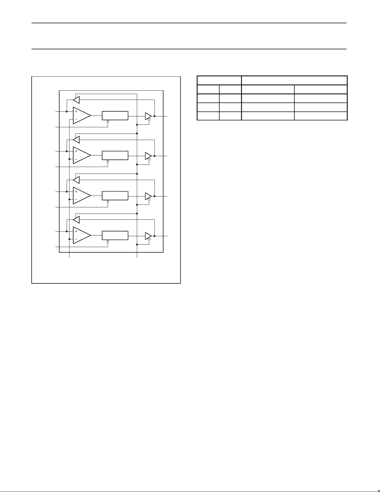
LOGIC SYMBOL
A0
LE0
A1
LE1
A2
LE2
LATCH
LATCH
LATCH
GTL2004
FUNCTION TABLE
INPUT INPUT/OUTPUT
DIR LEn A B
L H Inputs An = Bn
L L X NC
B0
B1
B2
H X Bn = An Inputs
H = HIGH voltage level
L = LOW voltage level
X = Don’t care
NC = No change
A3
LE3
GTLREF DIR
LATCH
B3
SW00319
1999 Jul 19
3
Page 4

Philips Semiconductors Product specification
VIDC input voltage
3
VODC output voltage
3
IOLCurrent into any output in the LOW state
VTTTermination voltage
V
V
Suppl
oltage
V
VIInput voltage
V
VIHHIGH-level input voltage
V
VILLOW-level input voltage
V
IOLLOW-level output current
Quad GTL/GTL+ to LVTTL/TTL
bidirectional latched translator
ABSOLUTE MAXIMUM RATINGS
In accordance with the Absolute Maximum System (IEC 134); voltages are referenced to GND (ground = 0V)
SYMBOL
V
CC
I
IK
I
OK
I
OH
T
stg
NOTES:
1. Stresses beyond those listed may cause permanent damage to the device. These are stress ratings only and functional operation of the
device at these or any other conditions beyond those indicated under “recommended operating conditions” is not implied. Exposure to
absolute-maximum-rated conditions for extended periods may affect device reliability .
2. The performance capability of a high-performance integrated circuit in conjunction with its thermal environment can create junction
temperatures which are detrimental to reliability. The maximum junction temperature of this integrated circuit should not exceed 150°C.
3. The input and output negative voltage ratings may be exceeded if the input and output clamp current ratings are observed.
DC supply voltage –0.5 to +4.6 V
DC input diode current VI < 0 –50 mA
p
DC output diode current VO < 0 –50 mA
Current into any output in the HIGH state A port –64 mA
Storage temperature range –60 to +150 °C
PARAMETER TEST CONDITIONS RATING UNIT
p
1
A port –0.5 to +7.0
B port –0.5 to +4.6
Output in OFF or HIGH state; A port
Output in OFF or HIGH state; B port
p
A port 128
B port 80
–0.5 to +7.0 V
–0.5 to +4.6 V
GTL2004
V
V
mA
mA
RECOMMENDED OPERATING CONDITIONS
SYMBOL
V
CC
REF
I
OH
T
amb
NOTE:
1. Unused control inputs must be held HIGH or LOW to prevent them from floating.
Supply voltage 0 3.6 V
pp
y v
p
HIGH-level output current B port –12 mA
Operating free-air temperature range –40 85 °C
PARAMETER TEST CONDITIONS MIN TYP MAX UNIT
p
p
p
1
GTL 1.14 1.2 1.26
GTL+ 1.35 1.5 1.65
GTL 0.74 0.8 0.87
GTL+ 0.87 1.0 1.10
A port 0 V
Except A port 0 5.5
A port V
Except A port 2
A port V
Except A port 0.8
A port 40 mA
B port 12 mA
REF
+ 50mV
REF
TT
– 50mV
1999 Jul 19
4
Page 5

Philips Semiconductors Product specification
VOHB port
V
V
C
pF
Quad GTL/GTL+ to LVTTL/TTL
bidirectional latched translator
DC ELECTRICAL CHARACTERISTICS
Over recommended operating conditions. V oltages are referenced to GND (ground = 0V).
SYMBOL PARAMETER TEST CONDITIONS
MIN TYP
p
VCC = 3.0 to 3.6V
VCC = 3.0V
A port VCC = 3.0V
OL
B port VCC = 3.0V
Control inputs VCC = 3.6V; VI = VCC or GND ± 1
A port VCC = 3.6V; VI = VTT or GND ± 1
I
I
B port
VCC = 0 or 3.6V; VI = 5.5 10
VCC = 3.6V; VI = V
VCC = 3.6V; VI = 0V –5
∆I
I
OFF
I
I
CC
C
EX
CC
A port VCC = 0V;V
B port VO = 5.5V; VCC = 3.0V 50 125 µA
A or B port VCC = 3.6V;VI = VCC or GND; IO = 0 3 mA
3
B port or control inputs VCC = 3.6V; VI = VCC –0.6V 500 µA
Control inputs VI = 3.0V or 0 3 pF
I
B port VO = 3.0V or 0 7.2
IO
A port VO = VTT or 0 4.6
NOTES:
1. All typical values are measured at V
2. The input and output voltage ratings may be exceeded if the input and output current ratings are observed.
= 3.3V and T
CC
amb
= 25°C.
3. This is the increase in supply current for each input that is at the specified TTL voltage level rather than V
IOH = –100µA VCC–0.2
;
IOH = –12mA 2.0
;
IOL = 40mA 0.4 V
;
IOL = 12mA 0.8 V
;
CC
or VO = 0 to 4.5V ± 100 µA
I
LIMITS
–40°C to +85°C
1
CC or GND.
GTL2004
UNIT
MAX
µA
± 1
p
AC CHARACTERISTICS (3.3V "0.3V RANGE)
LIMITS (GTL) LIMITS (GTL+)
SYMBOL PARAMETER WAVEFORM
t
PLH
t
PHL
t
PLH
t
PHL
t
PLH
t
PHL
Bn to An 2
An to Bn 3
LEn to Bn 1
VCC = 3.3V "0.3V
V
= 0.8V
REF
MIN TYP
2.0
1.8
4.4
4.7
3.5
3.4
1
MAX MIN TYP
2.8
2.5
6.5
5.8
4.9
4.2
NOTE:
1. All typical values are at V
AC SETUP REQUIREMENT (3.3V "0.3V RANGE)
Over recommended ranges of supply voltage.
= 3.3V and T
CC
amb
1
= 25°C.
LIMITS (GTL) LIMITS (GTL+)
SYMBOL PARAMETER WAVEFORM
VCC = 3.3V "0.3V
V
= 0.8V
REF
MIN MAX MIN MAX
tS(H)
tS(L)
th(H)
th(L)
Setup time (An to LEn) 4
Hold time (An to LEn) 4
1.3
1.5
0.0
0.0
tw(H) LEn pulse width 2 1.1 1.1 ns
NOTE:
1. These parameters are warranted but not production tested.
VCC = 3.3V "0.3V
V
= 1.0V
REF
1
2.0
1.8
4.4
4.5
3.5
3.4
VCC = 3.3V "0.3V
V
= 1.0V
REF
MAX
2.8
2.5
5.7
5.1
4.9
4.2
1.2
1.5
0.0
0.0
UNIT
ns
ns
ns
UNIT
ns
ns
1999 Jul 19
5
Page 6

Philips Semiconductors Product specification
Quad GTL/GTL+ to LVTTL/TTL
bidirectional latched translator
AC WAVEFORMS
VM = 1.5V at VCC w 3.0V, VM = VCC/2 at VCC v 2.7V for A ports and control pins
V
= V
M
V
X
V
Y
V
X
for B ports
Ref
= VOL + 0.3V at A ports
= VOH – 0.3V at A ports
= V
at B ports
REF
Bn
LEn
V
M
t
(H)
w
t
PHL
V
M
V
M
V
M
t
PLH
V
M
SW00333
Waveform 1. Propagation delay, Enable to Output and
Enable Pulse Width
t
PLH
3.0V or V
whichever is
less
0V
V
OH
V
OL
3.0V
CC
Output
ALL CONTROL INPUTS ARE TTL LEVELS.
ALL INPUT PULSES ARE SUPPLIED BY GENERATORS HAVING THE
FOLLOWING CHARACTERISTICS:
GTL2004
Input
Waveform 3. Propagation delay A port to B port
V
REF
t
PLH
1.5V 1.5V
PRR ≤ 10MHz, ZO = 50Ω, tr ≤ 2.5ns, tf ≤ 2.5ns.
V
REF
t
PHL
SW00469
V
TT
0V
V
OH
V
OL
Input
Output
VMV
VOLTAGE WAVEFORMS PULSE DURATION
V
= 1.5V for B port and 0.8V for A port
M
1.5V
t
PLH
V
REF
VOLTAGE WAVEFORMS PROPAGATION DELAY TIMES
B port to A port
V
M
1.5V
t
V
PHL
3.0V
V
REF
Waveform 2.
SW00470
3.0V or V
CC
0V
0V
V
OH
V
OL
Bn
LEn
V
V
M
M
t
(H)
s
t
(H) ts(H) tn(H)
n
V
M
V
V
M
Waveform 4. Data Setup and Hold Times
M
V
M
V
M
whichever is
less
0V
3.0V or V
whichever is
less
0V
SW00334
CC
1999 Jul 19
6
Page 7

Philips Semiconductors Product specification
Quad GTL/GTL+ to LVTTL/TTL
bidirectional latched translator
TEST CIRCUIT
V
CC
CC
V
O
50pF
C
L
of pulse generators.
OUT
V
PULSE
GENERATOR
I
D.U.T.
R
T
Test Circuit for switching times
DEFINITIONS
RL = Load resistor
CL = Load capacitance includes jig and probe capacitance
RT = Termination resistance should be equal to Z
Figure 1. Load circuitry for switching times
V
V
TT
GTL2004
RL = 500Ω
SW00471
PULSE
GENERATOR
V
I
D.U.T.
R
T
V
O
C
Figure 2. Load circuit for A outputs
L
SW00332
25Ω
30pF
1999 Jul 19
7
Page 8

Philips Semiconductors Product specification
Quad GTL/GTL+ to LVTTL/TTL
GTL2004
bidirectional latched translator
TSSOP16: plastic thin shrink small outline package; 16 leads; body width 4.4 mm SOT403-1
1999 Jul 30
8
Page 9

Philips Semiconductors Product specification
Quad GTL/GTL+ to LVTTL/TTL
bidirectional latched translator
GTL2004
NOTES
1999 Jul 30
9
Page 10

Philips Semiconductors Product specification
Quad GTL/GTL+ to LVTTL/TTL
bidirectional latched translator
Data sheet status
Data sheet
status
Objective
specification
Preliminary
specification
Product
specification
Product
status
Development
Qualification
Production
Definition
This data sheet contains the design target or goal specifications for product development.
Specification may change in any manner without notice.
This data sheet contains preliminary data, and supplementary data will be published at a later date.
Philips Semiconductors reserves the right to make changes at any time without notice in order to
improve design and supply the best possible product.
This data sheet contains final specifications. Philips Semiconductors reserves the right to make
changes at any time without notice in order to improve design and supply the best possible product.
[1]
GTL2004
[1] Please consult the most recently issued datasheet before initiating or completing a design.
Definitions
Short-form specification — The data in a short-form specification is extracted from a full data sheet with the same type number and title. For
detailed information see the relevant data sheet or data handbook.
Limiting values definition — Limiting values given are in accordance with the Absolute Maximum Rating System (IEC 134). Stress above one
or more of the limiting values may cause permanent damage to the device. These are stress ratings only and operation of the device at these or
at any other conditions above those given in the Characteristics sections of the specification is not implied. Exposure to limiting values for extended
periods may affect device reliability.
Application information — Applications that are described herein for any of these products are for illustrative purposes only. Philips
Semiconductors make no representation or warranty that such applications will be suitable for the specified use without further testing or
modification.
Disclaimers
Life support — These products are not designed for use in life support appliances, devices or systems where malfunction of these products can
reasonably be expected to result in personal injury . Philips Semiconductors customers using or selling these products for use in such applications
do so at their own risk and agree to fully indemnify Philips Semiconductors for any damages resulting from such application.
Right to make changes — Philips Semiconductors reserves the right to make changes, without notice, in the products, including circuits, standard
cells, and/or software, described or contained herein in order to improve design and/or performance. Philips Semiconductors assumes no
responsibility or liability for the use of any of these products, conveys no license or title under any patent, copyright, or mask work right to these
products, and makes no representations or warranties that these products are free from patent, copyright, or mask work right infringement, unless
otherwise specified.
Philips Semiconductors
811 East Arques Avenue
P.O. Box 3409
Sunnyvale, California 94088–3409
Telephone 800-234-7381
Copyright Philips Electronics North America Corporation 1999
All rights reserved. Printed in U.S.A.
Date of release: 07-99
Document order number: 9397 750 06247
1999 Jul 30
10
 Loading...