

Page 1

GS-R51212S
GS-R51515S
31W TRIPLE OUTPUT STEP-DOWN SWITCHING REGULATORS
Type V
GS-R51212S 15 to 40 V
GS-R51515S 15 to 40 V
i
V
o
+ 5,1 V 4,5 A
± 12V
+ 5,1 V 4,5 A
± 15 V
I
o
0,35 A
0,3 A
FEATURES
5.1V/4.5Aand ±12V/0.35A or ±15V/0.3Aoutput
voltages
±12 or ±15Vexternallyadjustable
High efficiency(81%typ.)
Short-circuitprotection
Reset output
Power Fail programmableinput
Inhibit/Enablecontrolinput
Soft-start
PCB or chassismounting
DESCRIPTION
The GS-R51212S and GS-R51515Sare versatile
triple output, high current step-down switching
regulators that provide +5.1V/4.5A output voltage
and an isolated ±12V/0.35A or ±15V/0.3A dual
output voltage.
They are ideal for microprocessor based boards
because power the logic and the communication
ports and have Reset output and Power Fail programmableinput for the correct system start-up.
The Inhibit/Enable pin allows the ON/OFF logic
functionwith TTL/CMOScompatibleinput signal.
The auxiliaryoutputs(±12Vor±15V)are externally
adjustablein a very widerange,i.e. from ±4.25Vto
±12.45V on GS-R51212S and from ±4.50V to
±15.25V (typical values)on GS-R51515S.
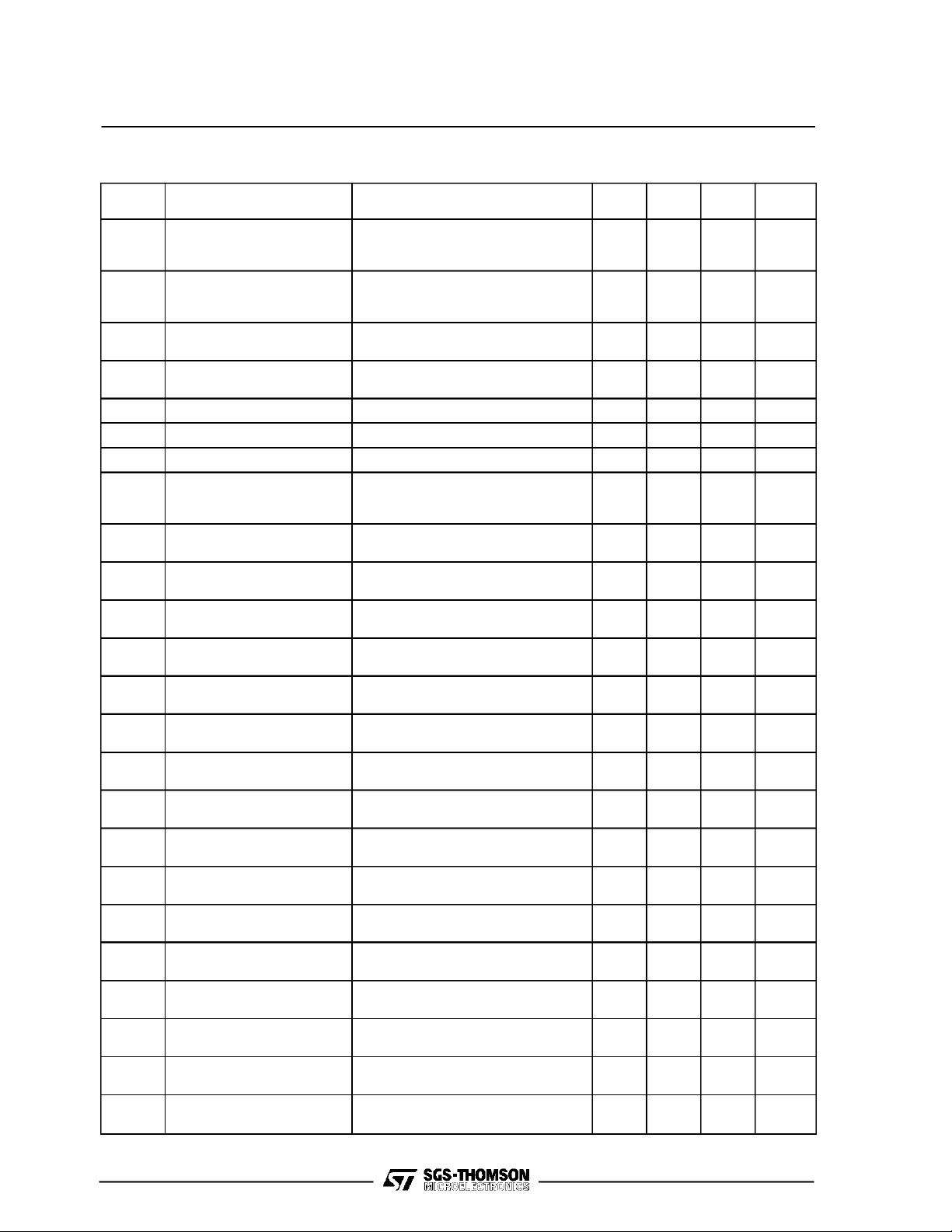
ABSOLUTE MAXIMUM RATINGS
Symbol Parameter Value Unit
V
i
I
rs
June 1994 1/8
DC Input Voltage 44 V
Reset Output Sink Current 20 mA
Page 2
GS-R51212S/GS-R51515S
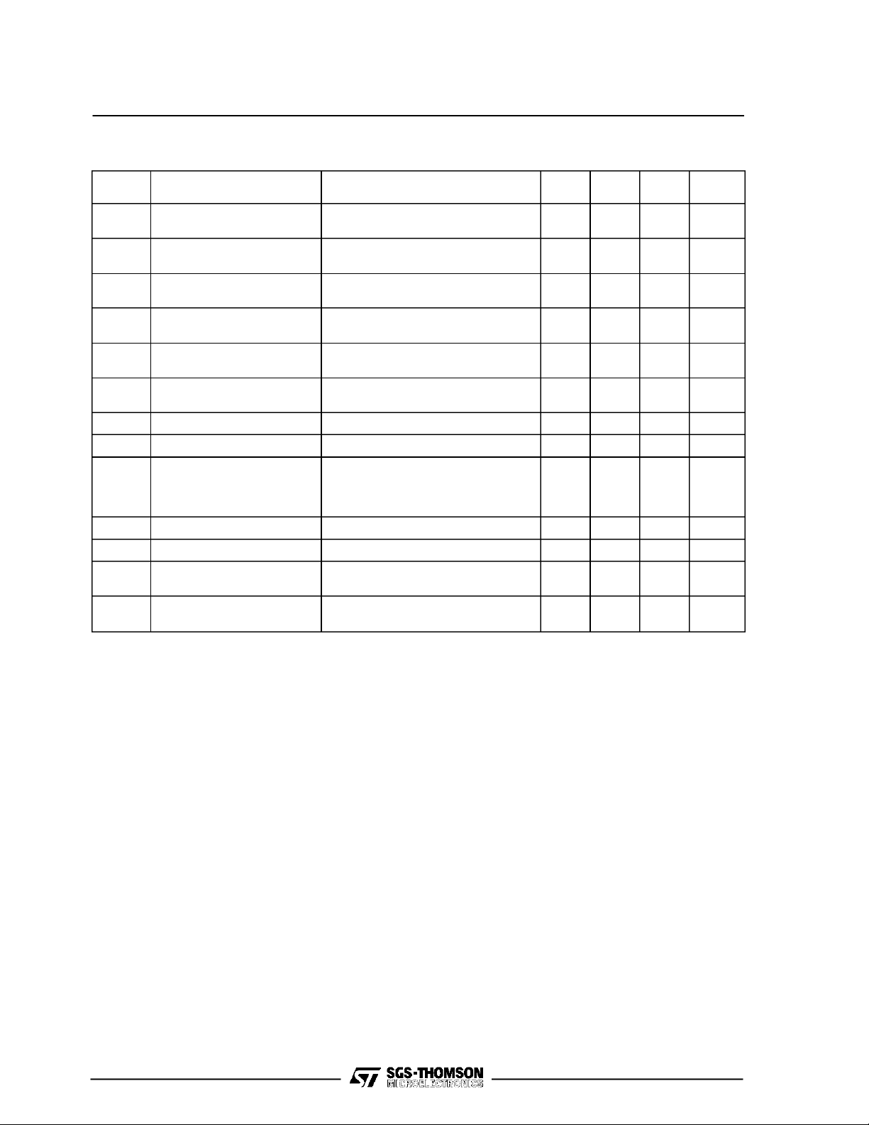
ELECTRICALCHARACTERISTICS (T
Symbol
V
Input Voltage
i
GS-R51212S
V
Input Voltage
i
GS-R51515S
l
Input ReflectedCurrent Vi= 24V I
ir
l
Input ReflectedCurrent Vi= 24V I
ir
V
δV
δV
δV
δV
V
l
V
V
V
V
V
V
V
or2,3
OL2,3
OO2,3
I
I
I
I
Enable Input Voltage Vi= 15 to 40V 0 0.8 V
ien
Enable Input Current Vi= 15 to 40V – 1 mA
ien
Inhibit Input Voltage Vi= 15 to 40V 1.2 +Vi V
iinh
Output Voltage 1 Vi= 15 to 40V Io1= 0 to 4.5A
o1
Output Voltage 2
o2
GS-R51212S
Output Voltage 2
o2
GS-R51515S
Output Voltage 3
o3
GS-R51212S
Output Voltage 3
o3
GS-R51515S
Output Ripple
or1
Voltage1
Output Ripple
Voltage2,3
Line Regulation 1 Vi= 15 to 40V Io1= 2.5A
OL1
Line Regulation 2,3 Vi= 15 to 40V
Load Regulation 1 Vi= 24V Io1= 0.5 to 4.5A
OO1
Load Regulation 2,3 Vi= 24V Io1= 2.5A
Output Current 1 Vi= 15 to 40V Vo1= 5.1V
o1
Output Current 2*
o2
GS-R51212S
Output Current 2*
o2
GS-R51515S
Output Current 2*
o2
GS-R51212S
Io2 Output Current 2*
GS-R51515S
Io3 Output Current 3*
GS-R51212S
Parameter Test Conditions Min Typ Max Unit
=25°C unless otherwise specified)
amb
Vo1= +5.1V Io1= 4.5A
15 40 V
Vo2= +12V Io2= 0.35A
Vo3= – 12V Io3= – 0.35A
Vo1= +5.1V
Vo2= +15V Io2= 0.3A
Io1
= 4.5A
15 40 V
Vo3= – 15V Io3= – 0.3A
= Full Load
No external input capacitor
Ci (external) = 100µF/50V
o1,2,3
o1,2,3
= Full Load
0.5 App
0.15 App
+5 +5.1 +5.2 V
Io2= 0 to 0.35/0.3A
Io3= 0 to – 0.35/– 0.3A
Vi= 15 to 40V Io1= 0 to 4.5A
+11.5 +12 +12.5 V
Io2= 0 to 0.35A Io3= 0 to – 0.35A
Vi= 15 to 40V Io1= 0 to 4.5A
+14.5 +15 +15.5 V
Io2= 0 to 0.3A Io3= 0 to – 0.3A
Vi= 15 to 40V Io1= 0 to 4.5A
– 11.5 – 12 – 12.5 V
Io2= 0 to 0.35A Io3= 0 to – 0.35A
Vi= 15 to 40V Io1= 0 to 4.5A
Io2= 0 to 0.3A
= 0 to – 0.3A
Io3
– 14.5 – 15 – 15.5 V
Vi= 24V Io1= 4.5A 30 50 mVpp
Vi= 24V I
= 0.35/0.3A 50 100 mVpp
o2,3
0.5 mV/V
I
= 0.35/0.3A
o2,3
I
o2,3
= 0.35/0.3A
Io1
= 2.5A
1 mV/V
2 mV/A
I
= 0.35/0.3A
o2,3
500 mV/A
I
= 0.05 to 0.35/0.3A
o2,Io3
0 4.5 A
I
= 0 to 0.35/0.3A
o2,3
Vi= 15 to 40V Io1= 0 to 4.5A
0 0.35 A
Vo2= +12V Io3= 0 to – 0.35A
Vi= 15 to 40V Io1= 0 to 4.5A
0 0.3 A
Vo2= +15V Io3= 0 to – 0.3A
Vi= 15 to 40V
Vo2= +12V Io3=0A
Vi= 15 to 40V Io1= 0 to 4.5A
= 0 to 4.5A
Io1
0 0.7 A
0 0.6 A
Vo2= +15V Io3=0A
Vi= 15 to 40V Io1= 0 to 4.5A
0 – 0.35 A
Vo3= – 12V Io2= 0 to 0.35A
2/8
Page 3
GS-R51212S/GS-R51515S
ELECTRICALCHARACTERISTICS (T
Symbol
I
I
I
I
osck1
I
osc1
I
osc2,3
t
t
R
T
T
* Note: whenoutput current is less than 50mA, outputripple voltage increases due todiscontinuous operation.
Output Current 3*
o3
GS-R51515S
Output Current 3*
o3
GS-R51212S
Output Current 3*
o3
GS-R51515S
Output Current
Limit 1
Output Short-circuit
Current 1
Output Short-circuit
Current 2,3
Soft-start time 10 ms
ss
Reset Time Delay 100 ms
dr
f
Switching Frequency Vi= 15 to 40V Vo1= 5.1V
s
η Efficiency Vi= 24V I
Thermal Resistance 7.5 °C/W
th
Operating Case
cop
TemperatureRange
Storage
stg
TemperatureRange
Parameter Test Conditions Min Typ Max Unit
=25°C unless otherwise specified) (cont’d)
amb
Vi= 15 to 40V Io1= 0 to 4.5A
Vo3= – 15V Io2= 0 to 0.3A
Vi= 15 to 40V Io1= 0 to 4.5A
Vo3= – 12V Io2=0A
Vi= 15 to 40V Io1= 0 to 4.5A
Vo3= – 15V Io2=0A
Vi= 15 to 40V Overload 5.5 A
Vi= 15 to 40V 3 A
Vi= 15 to 40V 0.8 A
Io1= 0.5 to 4.5A
Vo2= +12/+15V Vo3= – 12/– 15V
Io2,Io3= – 0.05 to – 0.35/– 0.3A
= Full Load 78 81 %
o1,2,3
0 – 0.3 A
0 – 0.7 A
0 – 0.6 A
0 +85 °C
– 40 +105 °C
100 kHz
3/8
Page 4

GS-R51212S/GS-R51515S
CONNECTION DIAGRAM AND MECHANICAL DATA
Package R.Dimensionsin mm (inches).
PIN DESCRIPTION
Pin Function Description
1 GND IN Return for input voltage source. Internallyconnected to pin 7.
2 EN.
3 P.F.
4 + Vin DC input voltage. Recommended maximum voltage is 40V.
5RT
6 Vo+ 5V Regulated +5.1V output voltage.
7 GND 1 Return for output 1 current path. Internally connected to pin 1.
8 Vo+ 12/15V Regulated+12 or +15V output.
9 Vo– 12/15V Regulated – 12 or – 15Voutput.
10 ADJ. External adjustment for output voltages ±12 and ±15V.
11 GND Aux. Return for ±12 and ±15V output current path.
4/8
Inhibit/Enable control input. The converter is ON (ENABLE) when the voltage applied to
this pin is lower than 0.8V. The converter is OFF (INHIBIT) when this pin is unconnected or
the input voltage is in the range of 1.2 to Vi.
Power Fail programmable input. If unconnected the Power Fail threshold voltage is 11V
with 1V hysteresis (factory setting).
Reset output (activehigh). When the supply voltage +Vin and the regulated output voltage
+Vo1are in the correct range this signalis generated after a delaytime of 100ms typical.
Page 5

GS-R51212S/GS-R51515S
USER NOTES
Input Voltage
The recommended operating maximum DC input
voltage is 40V inclusive of the ripple voltage. The
use of an external low ESR, high ripple current
capacitor located as close the module as possible
is recommended;suggestedvalue is 100µF/50V.
Soft-start
To avoid heavy inrush current the output voltage
risetime is typically 10ms in any conditionof load.
Power Fail-Reset Circuit
The module include a voltage sensing circuit that
may be used to generate a power-on/power-off
reset signal for a microprocessorsystem.
The circuit sense the input supply voltage and the
output generatedvoltageVo1(+5V)and willgenerate the required reset signal only when both the
sensed voltages have reached the required value
for correct systemoperation.
When both the supply voltage and the regulated
voltage are in the correct range the output Reset
signalis generatedaftera delaytime t
of100ms
DR
typical.
A latch assures that if a spike is present on the
sensed voltage the delay time circuit discharges
completelybefore initializationof anew reset cycle.
Reset output has internal pull-up resistor of
10kOhmconnected to Vo +5V pin.
Maximum sink output current is 20mA at
V
RESET(sat)
= 200mV.
Fig. 1 and fig.2 showreset waveforms.
Power Fail ProgrammableInput
This pin is internally connected via a divider to the
+Vin pin for Power Fail function.
The factory setting is for a value of 11V with 1V
hysteresis.
It is possibleto program a different value of Power
Fail threshold by connecting a resistor (Rpf) between pin 3 (Power Fail Input) and pin 1 (GND
Input).The value of Rpfmustbe calculatedaccording to the followingformula:
Rpf=
5.1
− 5.1
V
pf
− 0.191
34
=(kΩ)
whereVpf isthe desiredvalueof PowerFailthreshold voltage.
Exampe:Vpf = 24V (must not belower than 12V):
Rpf=
5.1
24 − 5.1
34
= 14kΩ
− 0.191
Figure1 - Resetand Power Fail waveforms.
5/8
Page 6

GS-R51212S/GS-R51515S
Figure2 - Resetand Power Fail waveforms.
AuxiliaryOutputs
Theauxiliaryoutputs(±12Vor±15V) areexternally
adjustabl e in s ymmetric way by conne cting a
resistor Ra between pin 10 (ADJ.) and pin 8
(Vo + 12/+15V),accordingtothefollowingformula:
V
− 4.229
GS−R51212S R
GS−R51515S R
= 32.66 ×
a
= 38.66 ×
a
o
12.485 − V
V
− 4.39
o
15.252 − V
o
o
whereVoisthe desired dual output voltage.
Example: V
= ±5V.
o
R
(GS−R51212S)=3.36kΩ
a
R
(GS−R51515S)=2.3kΩ
a
Example: Vo= ±10V.
R
(GS−R51212S)=75.8kΩ
a
R
(GS−R51515S)=41.3kΩ
a
6/8
Page 7

Figure3 - TypicalApplication.
GS-R51212S/GS-R51515S
Inhibit/EnableInput
The Inhibit/Enable function allows the ON/OFF
logiccontrol of the module.
The converter is ON (Enable) when the voltage
applied to pin 2 (EN.) and referred to pin 1 (GND
IN)is lower than 0.8V (TTL, CMOS, open collector
compatiblelevel).
Theconverteris OFF (Inhibit) when pin2 is unconnectedor the voltageappliedisin therangeof1.2V
to +Vin.Maximum sinking current is1mA.
Module Protection
The module is protected against occasional and
permanent short-circuits of the output pins to
ground,as wellas againstoutput currentoverload.
The main output (+5.1V) uses a foldback current
limiting;the outputcurrent decreaseswith increasing overload, reaching a minimum at short-circuit
condition.
This solution minimizes internalpower dissipation.
Theauxiliary outputs(±12Vor ±15V) use a current
limitingprotectioncircuitry.
Thermal characteristics
SometimestheGS-R51212SandGS-R51515Srequire an external heat-sinkdepending on both operating temperature conditions and power.
Before entering into calculations details,some basic conceptswill be explained to betterunderstand
the problem.
The thermal resistancebetween two points is representedby their temperaturedifferencein front of
a specifieddissipatedpower,and it is expressedin
Degree Centigrade per Watt (°C/W).
For the modules the thermal resistance case to
ambient is 7.5°C/W. This means that an internal
powerdissipationof1Wwillbring thecasetemperature at 7.5°C abovethe ambienttemperature.
The maximumcase temperatureis 85°C.
Let’ssuppose to have aGS-R51515Sthatdelivers
the maximumoutputpower of31.4W at anambient
temperatureof 40°C.
7/8
Page 8

GS-R51212S/GS-R51515S
The dissipated power in this operating condition is
about 7.4W (at typical efficiency of 81%), and the
case temperatureof the modulewill be:
T
= T
case
+ Pd× Rth= 40 + 7.4 × 7.5 = 95.5 °C
amb
This valueexceedsthemaximumallowedtemperature and an external heat-sink must be added. To
this purpose four holes (see mechanical drawing)
are providedon the metal surface of themodule.
Tocalculatethisheat-sink,let’sfirst determinewhat
the total thermal resistance should be:
T
R
case(max)
=
th
− T
P
d
amb
=
85 − 40
7.4
= 5.40 °C⁄W
This value is the resulting value of the parallel
connection of GS-R thermal resistance and of the
additionalheatsink thermal resistance.
R
(GSR) × Rth(Heatsink)
th
(GSR) + R
R
th
(Heatsink)
th
= 5.40°C/W
Tocalculatethethermalresistanceoftheadditional
heat-sink the following equation may be used:
R
(Heatsink)=
th
R
th(GSR)
(GSR)
th
− 5,40
5.40× 7.5
=
7.5 − 5.40
= 19.3 °C/W
5.40 ×
R
In instead of or in addition to the externalheatsink,
a forced ventilationwith an airspeed of about 200
linearfeet/minutecanbeusedreducingthethermal
resistanceof the moduleat the specifiedvalue.
Information furnished is believed to be accurate and reliable. However, SGS-THOMSON Microelectronics assumes no responsibility for the
consequences of use of such information nor for any infringement of patents or other rights of third parties which may result from its use. No
license is granted by implication or otherwise under any patentor patent rights of SGS-THOMSON Microelectronics. Specification mentioned
in this publication are subject to change without notice. This publication supersedes and replaces all information previously supplied.
SGS-THOMSON Microelectronics products arenot authorized for use as critical components inlife support devices orsystems without express
written approval of SGS-THOMSON Microelectronics.
1994 SGS-THOMSON Microelectronics –All Rights Reserved
Australia - Brazil - China - France - Germany - Hong Kong - Italy - Japan - Korea - Malaysia - Malta - Morocco - The Netherlands -
Singapore - Spain - Sweden - Switzerland - Taiwan - Thailand - United Kingdom - U.S.A.
SGS-THOMSON Microelectronics GROUP OF COMPANIES
8/8
 Loading...