

Page 1
Integrated
Circuit
Systems, Inc.
General Description Features
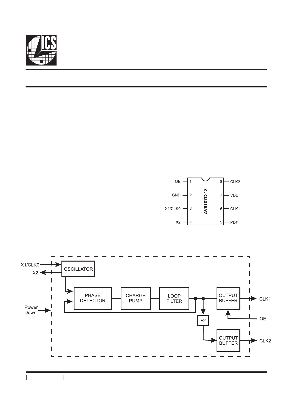
AV9107C-13
Block Diagram
CPU Frequency Generator
AV 9107-13 RevB052197
The AV9107C-13 offers a tiny footprint solution for
generating two simultaneous clocks. The AV9107C-13
uses a 20 MHz crystal to generate two PLL synthesis
outputs of 20 and 40 MHz. The Output enable pin will
tristate the 40 MHz output when low (maintaining the 20
MHz output runing in both logic levels). The power pin
takes the device to a low current condition, shutting off the
PLL and forcing both outputs low, when the PD# pin is low.
There is a built-in pull-up on both the OE and PD# inputs.
The device has advanced features which include on-chip
loop filters, tristate outputs, and power-down capability. A
minimum of external components - two decoupling capacitors
and an optional ferrite bead - are all that are required for jitterfree operation.
Patented on-chip Phase-Locked Loop with VCO
for clock generation
Provides two synthesized clocks
Generates 20 and 40 MHz output frequencies.
On-chip loop filter
Low power CMOS technology
Single +3.3 or +5 volt power supply
8-pin SOIC package
Pin Configuration
Note: Crystal is 20 MHz
Page 2
2
AV9107C-13
Pin Descriptions
Functionality
(at 14.318) MHz reference frequency input)
Frequency Accuracy and Calculation
The accuracy of the frequencies produced by the AV9107C
depends on the input frequency and the desired actual
output frequency. The formula for calculating the exact
output frequency is as follows:
For example, to calculate the actual output frequency for
a video monitor expecting a 44.900 MHz clock and using
a 14.318 MHz input clock, the closest A/B ratio is 69/22,
which gives an output of 44.906 MHz (within 0.02% of the
target frequency). Generally, the AV9107 can produce
frequencies within 0.1% of the desired output.
PIN
NUMBER
PIN NAME TYPE DESCRIPTION
1 OE Input Output Enable - Tristates the 40 MHz output when low. Pull-Up
2 GND PWR Ground.
3 X1/CLK0 Input Crystal Input or Input Clock frequency. Typically 20MHz crystal.
4 X2 Output Crystal Output (No Connect wh en clock used.).
5 PD# Input Power Down. Shuts off chip when low outputs are driven low. Internall pull-up.
6 CLK1 Output Clock 1 output 40MHz with 20MHz crysta l.
7 VDD PWR Digital power supply (+5V DC).
8 CLK2 Output
Clock2 output, div ided by 2 from clo ck1 output, for 20 MHz with 20MHz c rystal. Output is
synthesized.
OE CLK1 CLK2
0 20 MHz Tristate
1 20 MHz 40 MHz
Output Frequency = Input Frequency X
A
B
Allowable Input and Output Frequencies
The input frequency should be between 12 and 40 MHz
and the A/B ratio should not exceed 24. The output should
fall in the range of 12 to 80 MHz for CLK1 dnd CLK2. (See
specification for 3.3V and 5V condition details).
Output Enable
The Output Enable feature tristates the CLK1 output clock
pin. This places the selected output pins in a high inpedance
state to allow for system level diagnostic testing. The divideby-2 output of CLK2 remains active on the AV9107C-13 for
any OE state.
Power Down
The power down pin shuts off the entire chip to save
current. A few milliseconds are required to reach full
functioning speed from a power down state.
Where
A = 2, 3, 4 ... 128, and
B = 2, 3, 4 ...32.
Page 3

3
AV9107C-13
Note 1: Parameter is guaranteed by design and characterization. Not 100% tested in production.
Note2: AV9107C-13 with the power down pin low (active).
Note3: Absolute jitter measured as the shortest and longest period difference to the mean period of the sample set.
Electrical Characteristics at 5.0V
Operating VDD = +4.5V to +5.5V; TA =0°C to 70°C unless otherwise stated
Absolute Maximum Ratings
AVDD, VDD referenced to GND . . . . . . . . . . . . . . . 7V
Operating temperature under bias. . . . . . . . . . . . . . . . 0°C to +70°C
Storage temperature . . . . . . . . . . . . . . . . . . . . . . . . . . -65°C to +150°C
Voltage on I/O pins referenced to GND. . . . . . . . . . . GND -0.5V to VDD +0.5V
Power dissipation . . . . . . . . . . . . . . . . . . . . . . . . . . . . 0.5 Watts
Stresses above those listed under Absolute Maximum Ratings may cause permanent damage to the device.
This is a stress rating only and functional operation of the device at these or any other conditions above
those indicated in the operational sections of the specifications is not implied. Exposure to absolute
maximum rating conditions for extended periods may affect product reliability.
DC Characteristics
PARAMETER SYMBOL TEST CONDITIONS MIN TYP MAX UNITS
Input Low Voltage V
IL --0.8V
Input High Voltage V
IH 2.0 - - V
Input Low Current I
IL VIN=0V - 6.0 16.0 µA
Input High Current I
IH VIN=V
DD
2.0 - 2.0 µA
Output Low Voltage V
OL IOL=10mA - 0.25 0.40 V
Output High Voltage , Note 1 V
OH IOH=-30mA 2.4 3.25 - V
Output Low Current, Note 1 I
OL VOL=0.8V 22.0 35.0 - mA
Output High Current, Note 1 I
OH VOH=2.0V - -50.0 -35.0 mA
Supply Current I
DD No load - 18.0 40.0 mA
Output Freque ncy Change over
Supply and Temperature
F
d
With respect to typical frequency
Note 1
- 0.002 0.05 %
Stand by Supply Current I
DDSTDBY Not e 2 - 12.0 50.0 µ A
Pull-up Resistor, Note 1 R
pu VIN = VDD -1V - 380.0 800.0 k ohms
AC Characteristics
Output Rise Time 0.8 to 2.0V,
Note 1
T
r 15pF load - 0.65 1.60 ns
Output Fall Time 2.0 to 0.8V,
Note 1
T
f 15pF load - 0.55 1.2 ns
Rise Time 20% to 80% VDD,
Note 1
T
r 15pF load - 1.5 3.5 ns
Fall Time 80% to 20% VDD ,
Note 1
T
f 15pF load - 1.1 2.2 ns
Duty Cycle, Note 1 D
t 15pF load 45.0 - 55.0 %
Jitter, One Sigma, Note 1 T
jis 10,000 samples - 40.0 120. 0 ps
Jitter, Absolute, Notes 1, 3 T
jab 10,000 samples -500.0 200 500.0 ps
Input Freq uency, Note 1 F
i 14 20 40 MHz
Output Frequency, Note 1 F
o C lock1 28 40 80 MHz
Power-up Time, Note 1 T
pu -130300µs
Page 4

4
AV9107C-13
Electrical Characteristics at 3.3V
Operating V
DD
= +3.0V to +3.7V; TA =0°C to 70°C unless otherwise stated
DC Characteristics
PARAMETER SYMBOL TEST CONDITIONS MIN TYP MAX UNITS
Input Low Voltage V
IL --0.20V
DD
V
Input High Voltage V
IH 0.7VDD - - V
Input Low Current, Note1 I
IL VIN=0V - 2.5 7.0 µA
Input High Current, Note 1 I
IH VIN=V
DD
-2.0 - 2.0 µ A
Output Low Voltage, Note 1 V
OL IOL=6mA - 0.15 0.1xV
DD
V
Output High Voltage , Note 1 V
OH IOH=-5mA 0.85xV
DD
0.92xV
DD
-V
Output Low Current, Note 1 I
OL VOL=0.2V
DD
15.0 22.0 - m A
Output High Current, Note 1 I
OH VOL=0.7V
DD
- -17.0 -10.0 mA
Supply Current, Note 1 I
DD Unl oaded - 11.0 25.0 mA
Standby Supply Current,
Notes 1, 2
I
DDSTDBY - 13.0 40.0 µ A
Output Frequenc y Change over
Supply and Temperature, Note1
F
d
With respect to typical
frequency
- 0.002 0.01 %
Pull-up Resistor, Note 1 R
pu VIN = VDD - 0.5V - 0 .55 1.0 M ohms
AC Characteristics
Rise Time 20% to 80% VDD,
Note 1
T
r 15pF load - 2.0 3.4 ns
Fall Time 80% to 20% VDD ,
Note 1
T
f 15pF load - 1.2 2.2 ns
Duty Cycle, Note 1 D
t 15pF load @ 50% 42 - 52 %
Jitter, One Sigma, Note 1 T
jis 10,000 samples - 40.0 120.0 ps
Jitter, Absolute, Notes 1, 3 T
jab 10,000 sampl es 500.0 2 00 500.0 ps
Input Frequ ency, Note 1 F
i 12 20 25 MHz
Output Frequency, Note 1 F
o Clock1 24 40 50 MHz
Power-up Time, Note 1 T
pu - 2 65 500 µs
Note 1: Parameter is guaranteed by design and characterization. Not 100% tested in production.
Note2: AV9107C-13 with the power down pin low (active).
Note3: Absolute jitter measured as the shortest and longest period difference to the mean period of the sample set.
Page 5

5
AV9107C-13
Ordering Information
AV9107C-13CS08
Example:
8-Pin Plastic SOIC Package
XXX XXXX-PPP M X#W
Lead Count & Package Width
Lead Count=1, 2 or 3 digits
W=.3 SOIC or .6 DIP; None=Standard Width
Package Type
S=SOIC
Pattern Number (2 or 3 digit number for parts with ROM code patterns, if applicable)
Device Type (consists of 3 or 4 digit numbers)
Prefix
ICS, AV=Standard Device; GSP=Genlock Device
 Loading...