

Page 1
™
GS9032
GENLINX
II
Digital Video Serializer
DATA SHEET
FEATURES
• SMPTE 259M and 540Mb/s compliant
• serializes 8-bit or 10-bit data
• autostandard, adjustment free operation
• minimal external components (no loop filter
components required)
• isolated, quad output, adjustable cable driver
• power saving secondary cable driver disable
• 3.3V and 5.0V CMOS/TTL compatible inputs
• lock detect indication
• SMPTE scramble and NRZI coding bypass option
• EDH support with GS9001, GS9021 or EDH FPGA code
APPLICATION
SMPTE 259M and 540Mb/s parallel to serial interfaces for
video cameras, VTRs, and signal generators; generic
parallel to serial conversion.
DESCRIPTION
The GS9032 encodes and serializes SMPTE 125M and
244M bit parallel digital video signals, and other 8-bit or
10-bit parallel formats. This device performs sync
detection, parallel to serial conversion, data scrambling
(using the X
9
+ X4 + 1 algorithm), 10x parallel clock
multiplication and conversion of NRZ to NRZI serial data.
The GS9032 features auto standard and adjustment free
operation for data rates to 540Mb/s with a single VCO
resistor. Other features include a lock detect output, NRZI
encoding, SMPTE scrambler bypass, a sync detect disable,
and an isolated quad output cable driver suitable for driving
75Ω loads. The complementary cable driving output swings
can be adjusted independently or the secondary differential
cable driver can be powered down.
The GS9032 requires a single +5 volt or -5 volt supply and
typically consumes 675mW of power while driving four 75Ω
loads.
ORDERING INFORMATION
PART NUMBER PACKAGE TEMPERATURE
GS9032 - CVM 44 pin TQFP 0°C to 70°C
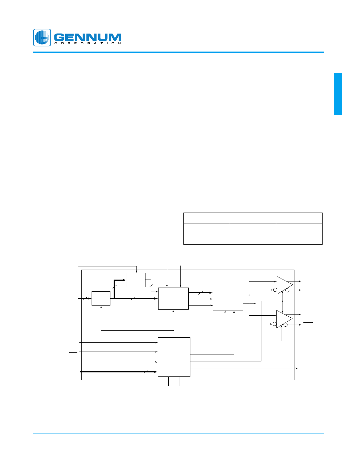
GS9032
DATA
IN
(PD0-PD9)
PARALLEL CLOCK
INPUT (PCLKIN)
AUTO/MANUAL SELECT
(AUTO/MAN)
LOOP BANDWIDTH
CONTROL (LBWC)
DATA RATE SELECT
SS[2:0]
SYNC DETECT DISABLE (SYNC DIS)
SYNC
DETECT
10
10
INPUT
LATCH
8
RESET
2
3
BYPASS
SMPTE
SCRAMBLER
S
CLK
PLL
R
VCO+RVCO-
BYPASS
/10
BLOCK DIAGRAM
GS9032 - CTM 44 pin TQFP Tape 0°C to 70°C
SDO0
10
RESET
PARALLEL
to SERIAL
CONVERTER
&
NRZ to NRZI
S
CLK
P
SDO0
SERIAL
DIGITAL
OUTPUTS
SDO1
SDO1
LOAD
SDO1
ENABLE
MUTE
LOCK
DETECT
(LOCK DET)
Revision Date: January 2001 Document No. 521 - 96 - 05
GENNUM CORPORATION P.O. Box 489, Stn. A, Burlington, Ontario, Canada L7R 3Y3
Tel. +1 (905) 632-2996 Fax. +1 (905) 632-5946 E-mail: info@gennum.com
www.gennum.com
Page 2
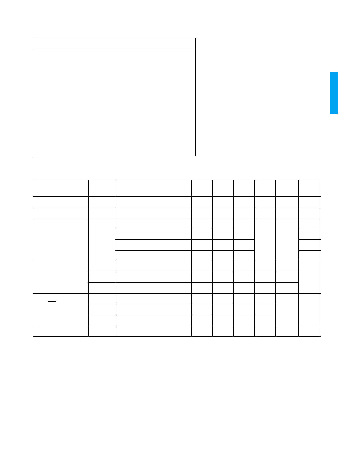
ABSOLUTE MAXIMUM RATINGS
PARAMETER VALUE
Supply Voltage (V
Input Voltage Range (any input) V
= VCC-VEE)5.5V
S
EE<VIN<VCC
DC Input Current (any one input) 5mA
Power Dissipation (V
θ
j-a
θ
j-c
= 5.25V) 1200mW
CC
42.5°C/W
6.4°C/W
Maximum Die Temperature 125°C
Operating Temperature Range 0°C ≤ T
Storage Temperature Range -65°C ≤ T
≤ 70°C
A
≤ 150°C
S
Lead Temperature (soldering, 10 sec) 260°C
DC ELECTRICAL CHARACTERISTICS
VCC = 5V, VEE = 0V, TA =0°C to 70°C unless otherwise specified.
PARAMETER SYMBOL CONDITIONS MIN TYP MAX UNITS NOTES
Positive Supply Voltage V
Power (System Power) P V
Operating Range 4.75 5.00 5.25 V 1
CC
= 5.0V, T = 25°C (4 outputs) - 675 - mW 5
CC
GS9032
TEST
LEVEL
Supply Current
Data & Clock Inputs
(PD[9:0] PCLKIN)
SYNC DIS
Logic Input Levels
(Auto/Man
, SS[2:0]
Bypass, RESET)
Lock Detect Output V
Ι
V
V
V
V
VCC = 5.25V (4 outputs) - - 180 mA 1
CC
= 5.0V, T = 25°C (4 outputs) - 135 - 1
V
CC
= 5.25V (2 outputs) - - 160 1
V
CC
V
= 5.0V, T = 25°C (2 outputs) - 110 - 7
CC
Logic Input High (wrt VEE)2.4--V 1
IH
Logic Input Low (wrt VEE)--0.8V
IL
Input Current - - 8.0 µA
Ι
L
Logic Input High (wrt to VEE)2.4--V 1
IH
Logic Input Low (wrt to VEE)--0.8V
IL
Input Current - - 5.0 µA
Ι
L
Sinking 500µA - - 0.4 V 1
OL
TEST LEVELS
1. Production test at room temperature and nominal supply voltage with guardbands for supply and temperature ranges.
2. Production test at room temperature and nominal supply voltage with guardbands for supply and temperature ranges using correlated
test.
3. Production test at room temperature and nominal supply voltage.
4. QA sample test.
5. Calculated result based on Level 1,2, or 3.
6. Not tested. Guaranteed by design simulations.
7. Not tested. Based on characterization of nominal parts.
8. Not tested. Based on existing design/characterization data of similar product.
GENNUM CORPORATION
2
521 - 96 - 05
Page 3
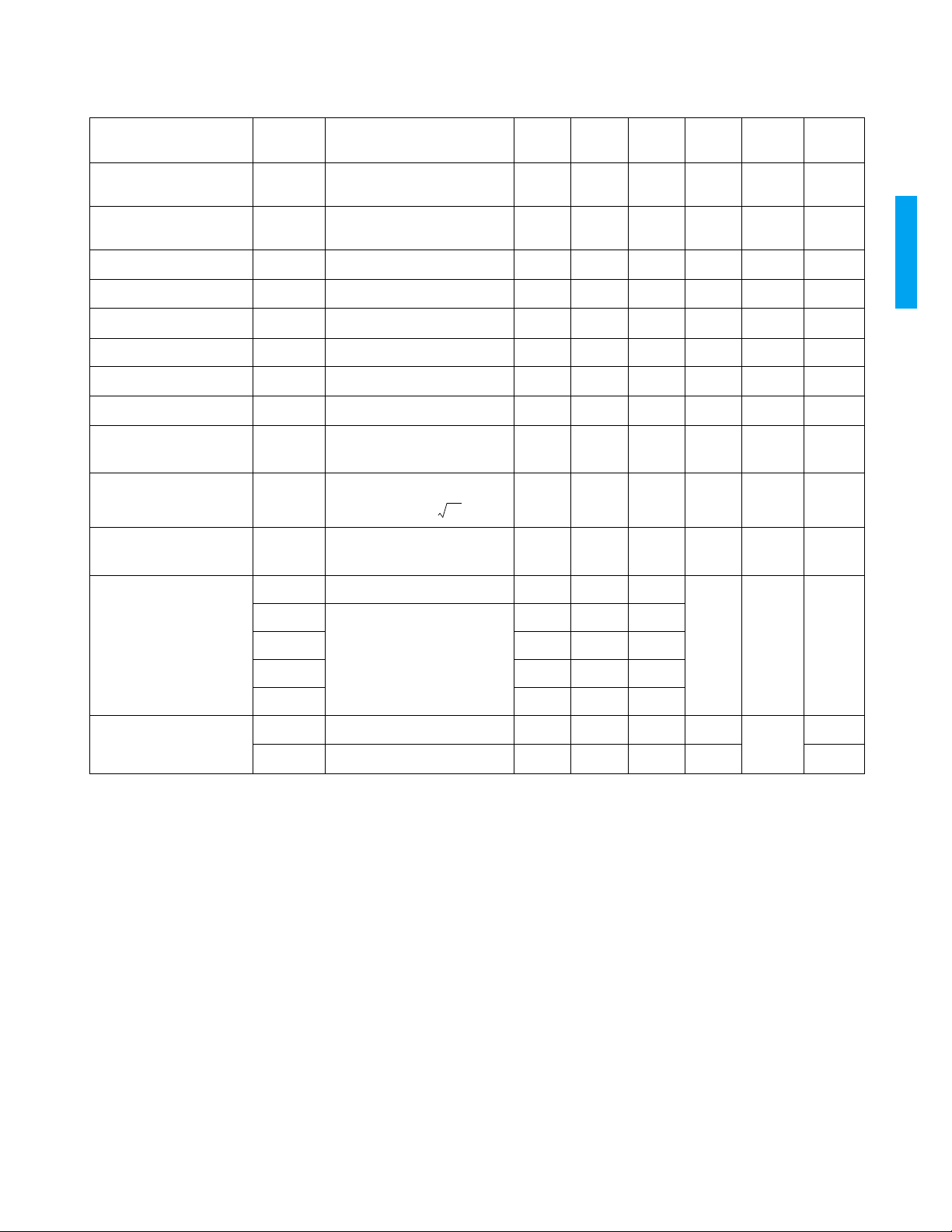
AC ELECTRICAL CHARACTERISTICS
VCC = 5V, VEE = 0V, TA =0°C to 70°C unless otherwise specified.
PARAMETER SYMBOL CONDITIONS MIN TYP MAX UNITS NOTES
R
Serial Data Bit Rate BR
SDO
VCO
= 374
Ω
143 - 540 Mb/s SMPTE
TEST
LEVEL
259M
Serial Data Outputs Signal
V
SDO
R
LOAD
= 37.5Ω, R
SET
= 54.9
Ω
740 800 860 mVp-p 1
Swing
Min. Swing (adjusted) V
Max. Swing (adjusted) V
SD Rise/Fall Times t
SDOMINRLOAD
SDOMAXRLOAD
, t
r
f
= 37.5Ω, R
= 37.5Ω, R
SET
SET
= 73.2
= 43.2
Ω
Ω
- 600 - mVp-p 7
-1000-mVp-p 1
20% - 80% 400 - 700 ps 7
SD Overshoot/Undershoot - - 7 % 1 7
Output Return Loss O
Lock Time t
Min. Loop Bandwidth BW
Typical Loop Bandwidth BW
Max. Loop Bandwidth BW
LOCK
at 540MHz 15 - - dB 1 7
RL
Worst case - - 5 ms 6
270Mb/s
MIN
LBWC = Grounded : BW
270Mb/s
TYP
LBWC = Floating : BW
270Mb/s
MAX
LBWC = V
CC
: 10 BW
10
MIN
MIN
MIN
- 220 - kHz 7
- 500 - kHz 7
-1.7-MHz 7
1
GS9032
Intrinsic Jitter (6
σ)
143Mb/s LBWC = floating - 0.07 - UI 1
177Mb/s LBWC = V
CC
-0.07-
270Mb/s - 0.08 -
360Mb/s - 0.09 -
540Mb/s - 0.11 -
Data & Clock Inputs
(PD[9:0] PCLKIN)
t
t
Setup Time at 25°C2.5--ns 1
SU
Hold Time at 25°C2.0--ns 1
H
TEST LEVELS
1. Production test at room temperature and nominal supply voltage with guardbands for
supply and temperature ranges.
2. Production test at room temperature and nominal supply voltage with guardbands for
supply and temperature ranges using correlated test.
3. Production test at room temperature and nominal supply voltage.
4. QA sample test.
5. Calculated result based on Level 1,2, or 3.
6. Not tested. Guaranteed by design simulations.
7. Not tested. Based on characterization of nominal parts.
8. Not tested. Based on existing design/characterization data of similar product.
NOTES
1. Depends on PCB layout.
GENNUM CORPORATION
3
521 - 96 - 05
Page 4

PIN CONNECTIONS
PD9
PD8
PD7
PD6
PD5
PD4
PD3
PD2
PD1
PD0
PCLKIN
EE
SYNC DIS
V
LF-
44 43 42 41 40 39 38 37 36 35 34
1
2
3
4
5
6
7
8
9
10
11
12 13 14 15 16 17 18 19 20 21 22
EE3
CC3
OSC
V
V
C
LF+
LBWC
GS9032
TOP VIEW
SS1
SS2
EE
VCO-
V
CC2
V
VCO+
R
R
NC
2
EE
V
LOCK DET
SDO1 ENABLE
EE1
V
SSO
V
CC1
R
33
32
31
30
29
28
27
26
25
24
23
SET0
RESET
AUTO/MAN
BYPASS
R
SET1
V
EE
SDO1
SDO1
V
EE
SDO0
SDO0
V
EE
GS9032
PIN DESCRIPTIONS
NUMBER SYMBOL TYPE DESCRIPTION
1-10 PD9 - PD0 I CMOS or TTL compatible parallel data inputs. PD0 is the LSB and PD9 is the MSB.
11 PCLKIN I CMOS or TTL compatible parallel clock input.
12 V
13 V
14 C
EE3
CC3
OSC
15, 16, 21 SS2, SS1, SS0 I Data rate selection when in manual mode. These pins are not used in auto mode.
17 V
18 V
CC2
EE2
19 SDO1 ENABLE I Enable pin for the secondary cable driver (SDO1 and SDO1
20 LOCK DET O TTL level which is high when the internal PLL is locked.
22 R
23, 26, 29 V
24, 25 SDO0
SET0
EE
, SDO0 O Primary, current mode, 75Ω cable driving output (inverse and true)
- Most negative power supply connection for parallel data and clock inputs.
- Most positive power supply connection for parallel data and clock inputs.
I Master Timer Capacitor. A capacitor should be added to decrease the system clock
frequency when an external capacitor is used across LF+ and LF- (NC if not used).
- Most positive power supply connection for internal logic and digital circuits.
- Most negative power supply connection for internal logic and digital circuits.
). Connect to most negative
power supply to enable. Leave open to disable (do NOT connect to V
CC
I External resistor used to set the data output amplitude for SDO0 and SDO0.
- Most negative power supply connection for shielding (not connected).
).
27, 28 SDO1
30 R
GENNUM CORPORATION
, SDO1 O Secondary, current mode, 75Ω cable driving output (inverse and true)
SET1
I External resistor used to set the data output amplitude for SDO1 and SDO1.
4
521 - 96 - 05
Page 5

PIN DESCRIPTIONS
NUMBER SYMBOL TYPE DESCRIPTION
31 BYPASS I When high, the SMPTE Scrambler and NRZ encoder are bypassed.
32 AUTO/MAN
I Autostandard or manual mode selectable operation.
33 RESET I Resets the scrambler when asserted.
34 V
35 V
36, 38 R
VCO
CC1
EE1
+, R
VCO
- Most positive power supply connection for analog circuits.
- Most negative power supply connection for analog circuits.
- I Differential VCO current setting resistor that sets the VCO frequency.
37 NC I No Connect.
39, 43 V
EE
- Most negative power supply connection (substrate).
40 LBWC I TTL level loop bandwidth control that adjusts the PLL bandwidth to optimize for lowest
jitter. If the pin is set to ground the loop bandwidth is BW
loop bandwidth is approximately 3 BW
approximately10 BW
MIN
, if the pin is tied to VCC the loop bandwidth is
MIN
. If the pin is left floating, the
MIN
41, 42 LF+, LF- I Differential loop filter pins to optimize loop transfer performance at low loop bandwidths
(NC if not used).
44 SYNC DIS I Sync detect disable. Logic high disables sync detection. Logic low allows 8 bit operation
by mapping 000-003 to 000 and 3FC-3FF to 3FF.
GS9032
TYPICAL PERFORMANCE CURVES
500
490
480
470
460
5.25 RISE
450
4.75 FALL
RISE / FALL TIME (ps)
440
430
420
020406080
Fig. 1 Rise/Fall Times vs. Temperature Fig. 2 Supply Current vs. Temperature (SDO0 & SDO1 ON)
4.75 RISE
5.0 RISE
5.0 FALL
5.25 FALL
TEMPERATURE (˚C)
(V
= 5V, TA = 25°C unless otherwise shown. Guard band tested to 70°C only.)
S
155
150
145
5.25
140
5.0
135
CURRENT (mA)
4.75
130
125
020406080
TEMPERATURE (˚C)
GENNUM CORPORATION
5
521 - 96 - 05
Page 6

1.01
E
A
V
S
A
V
4ƒ
sc
DATA
STREAM
ACTIVE VIDEO
& H BLANKING
T
R
S
ACTIVE
VIDEO
T
R
S
T
R
S
ACTIVE VIDEO
& H BLANKING
4:2:2
DATA
STREAM
E
A
V
S
A
V
H
BLNK
H
BLNK
SYNC
DETECT
SYNC
DETECT
SYNC
DETECT
XXX 3FF 000 000 XXX ••• ••• XXX 3FF 000 000 XXX •••
PCLK IN
PDN
1.005
1.000
OUTPUT SWING (V)
0.995
0.99
5.25
5.0
4.75
020406080
TEMPERATURE (˚C)
Fig. 3a Output Swing vs. Temperature (1000mV)
0.8075
0.805
0.8025
0.800
0.7975
OUTPUT SWING (V)
0.795
0.7925
020406080
5.25
5.0
4.75
TEMPERATURE (˚C)
Fig. 5 Timing Diagram
160
140
120
100
80
60
LF+ — LF- (mV)
40
20
0
020406080
TEMPERATURE (˚C)
GS9032
Fig. 3b Output Swing vs. Temperature (800mV)
t
t
CLKL
=
CLKH
PARALLEL
CLOCK
PLCK
GENNUM CORPORATION
PARALLEL
DATA
PDn
Fig. 4 Waveforms
t
SU
50%
t
HOLD
Fig. 6a Loop Filter Voltage vs. Temperature (360 Mode)
40
20
0
-20
LF+ — LF- (mV)
-40
-60
020406080
TEMPERATURE (˚C)
Fig. 6b Loop Filter Voltage vs. Temperature (540 Mode)
6
521 - 96 - 05
Page 7

3500
3000
2500
2000
1500
LOOP BANDWIDTH (kHz)
1000
500
0
0 143 177 270 360 540
LBWC to V
CC
LBWC FLOATING
LBWC GROUNDED
DATA RATE (Mb/s)
Fig. 7 Loop Bandwidth vs. Data Rate
600
500
400
300
200
JITTER p-p (ps)
GS9032
Fig. 10 Output Eye Diagram (270Mb/s)
100
For a data rate of 270Mb/s
0
GROUNDED FLOATING V
LOOP BANDWIDTH CONTROL (LBWC)
Fig. 8 Output Jitter vs. LBWC
500
400
300
200
JITTER p-p (ps)
100
0
0 100 200 300 400 500 600
DATA RATE (Mb/s)
Fig. 9 Output Jitter vs. Data Rate
(Optimum LBW Setting)
CC
Fig. 11 Output Eye Diagram (540Mb/s)
GENNUM CORPORATION
7
521 - 96 - 05
Page 8

DETAILED DESCRIPTION
The GS9032 Serializer is a bipolar integrated circuit used to
convert parallel data into a serial format according to the
SMPTE 259M standard. The device encodes both eight and
ten bit TTL-compatible parallel signals producing serial
data rates up to 540Mb/s. It operates from a single five volt
supply and is packaged in a 44 pin TQFP.
Functional blocks within the device include the input
latches, sync detector, parallel to serial converter, SMPTE
scrambler, NRZ to NRZI converter, internal cable driver, PLL
for 10x parallel clock multiplication and lock detect. The
parallel data (PD0-PD9) and parallel clock (PCLKIN) are
applied via pins 1 through 11 respectively.
1. SYNC DETECTOR
The sync detector makes the system compatible with eight
or ten bit data. It looks for the reserved words 000-003 and
3FC-3FF in ten bit hexadecimal, or 00 and FF in eight bit
hexadecimal, used in the TRS-ID sync word. When the
occurrence of either all zeros or all ones at inputs PD2-PD9
is detected, the lower two bits PD0 and PD1 are forced to
zeros or ones respectively. For non-SMPTE standard
parallel data, the sync detector can be disabled through a
logic input, Sync Detect Disable (44).
2. SCRAMBLER
The scrambler is a linear feedback shift register used to
pseudo-randomize the incoming serial data according to
the fixed polynomial (X
9+X4
+1). This minimizes the DC
component in the output serial data stream. The NRZ to
NRZI converter uses another polynomial (X+1) to convert a
long sequence of ones to a series of transitions, minimizing
polarity effects. These functions can be disabled by setting
the BYPASS pin (31) high.
3. PHASE LOCKED LOOP
The PLL performs parallel clock multiplication and provides
the timing signal for the serializer. It is composed of a
phase/frequency detector (with no dead zone), charge
pump, VCO
,
a divide-by-ten counter, and a divide-by-two
counter.
The phase/frequency detector allows a wider capture range
and faster lock time than with a phase discriminator alone.
The discrimination of frequency eliminates harmonic
locking. With this type of discriminator, the PLL can be overdamped for good stability without sacrificing lock time.
The charge pump delivers a 'charge packet' to the loop
filter which is proportional to the system phase error.
Internal voltage clamps are used to constrain the loop filter
voltage between approximately 1.8 and 3.4 volts.
The VCO is a differential low phase noise, factory trimmed
design that provides increased immunity to PBC noise and
precise control of the VCO centre frequency. The VCO can
operate in excess of 800MHz and has a pull range of ±15%
about the centre frequency. The single external resistor,
R
, sets the VCO frequency
VCO
4. VCO CENTRE FREQUENCY SELECTION
For a given R
value, the VCO can oscillate at one of two
VCO
(see Figure 12)
.
frequencies. When SS0=logic 1, the VCO centre frequency
corresponds to the ƒ
centre frequency corresponds to the ƒ
approximately 1.5 x ƒ
800
700
600
500
400
300
200
VCO FREQUENCY (MHz)
100
0
0 200 400 600 800 1000 1200 1400 1600 1800
The recommended R
applications is 374Ω (
curve. For SS0=logic 0, the VCO
L
curve (ƒH is
H
).
L
ƒ
H
SSO=0
ƒ
L
SSO=1
R
(Ω)
VCO
Fig. 12
value for auto rate SMPTE 259M
VCO
see the Typical Application Circuit
This value prevents false standards indication in auto mode.
For non-SMPTE applications (where data rates are x2
harmonically related) use Figure 12 to determine the R
VCO
values.
The VCO and an internal divider generate the PLL clock.
Divider moduli of 1, 2, and 4 allow the PLL to lock to data
rates from 143Mb/s to 540Mb/s. The divider modulus is set
by the AUTO/MAN
further details
, and SS[2:0] pins (
see Truth Table for
). In addition, a manually selectable modulus
8 divider allows operation at data rates as low as 18Mb/s
when R
is increased to 1kΩ.
VCO
When the loop is not locked, the lock detect circuit mutes
the serial data outputs. When the loop is locked, the Lock
Detect output is available from pin 20 and is HIGH.
The true and complement serial data, SDO and SDO
, are
available from pins 24, 25, 27 and 28. These outputs drive
four 75Ω co-axial cables with SMPTE level serial digital
video signals. To disable the outputs from pins 27 and 28
(SDO1
, SDO1), remove the resistor connected to the R
SET1
pin (30) and float the SDO1 ENABLE pin (19).
NOTE: Do NOT connect pin 19 to V
R
calculation:
SET
SET
1.154 R
---------------------------------------=
|| Z
V
where R
LOAD
= R
R
PULL-UP
×
SDO
CC
LOAD
.
GS9032
).
GENNUM CORPORATION
8
521 - 96 - 05
Page 9

TYPICAL APPLICATION CIRCUIT
V
CC
LBWC
(SMPTE Auto Mode)
J1
374
100n
V
CC
44 43 42 41 40 39 38 37 36 35 34
1
PD9
PD8
PD7
PD6
PD5
PD4
PD3
PD2
PD1
PD0
PCLKIN
SYNC_DIS
EE3VCC3
V
PARALLEL
DATA
INPUTS
PARALLEL
CLOCK
INPUT
2
3
4
5
6
7
8
9
10
11
12 13 14 15 16 17 18 19 20 21 22
100n
All resistors on ohms,
all capacitors in farads,
unless otherwise stated.
*
See Truth Table for settings. NC in auto mode.
V
220
CC
V
CC
100n
1µ
J1
54.9
75
L
75
R
L
1µ
J2
R
L
1µ
J3
R
75
75
V
CC
L
1µ
J4
R
V
CC
L = 8.2nH
R = 75Ω
LF+
SS2
SS2*
V
CC
EE
V
LBWC
GS9032
CC2VEE2
SS1
V
SS1*
VCO
R
0
NC
VCO+
R
AUTO/MAN
BYPASS_EN
SDO1_EN
LOCK
10k
EE1
V
SS0
SS0*
CC1
V
RESET
R
SET1
V
SDO1
SDO1
V
SDO0
SDO0
V
SET0
R
54.9
EE
EE
EE
33
32
31
30
29
28
27
26
25
24
23
RESET
100n
EE
LF-
V
)
OSC
NC (C
V
CC
100n
GS9032
LOCK
TRUTH TABLE (Manual Mode)
DATA RATE
(Mb/s)
SS2 SS1 SS0
DIVIDER
MODULI
143 0 0 0 4 ƒ
177 0 0 1 2 ƒ
270 0 1 0 2 ƒ
360 0 1 1 1 ƒ
540 1 0 0 1 ƒ
451018ƒ
681108ƒ
VCO
FREQUENCY
H
L
H
L
H
L
H
GENNUM CORPORATION
9
521 - 96 - 05
Page 10

PACKAGE DIMENSIONS
12.00
10.00
1.00
0.10
PIN 1
0.80
0.30
10.00
0.127
12.00
1.10
12˚ TYP
12˚ TYP
0.08 MIN.
RADIUS
0.20 MIN
0.20 MAX
0 MIN
RADIUS
7˚ MAX
0˚ MIN
0.60
±0.15
0.20 MIN
44 pin TQFP
All dimensions in millimetres
GS9032
CAUTION
ELECTROSTATIC
SENSITIVE DEVICES
DO NOT OPEN PACKAGES OR HANDLE
EXCEPT AT A STATIC-FREE WORKSTATION
DOCUMENT IDENTIFICATION
DATA SHEET
The product is in production. Gennum reserves the right to make
changes at any time to improve reliability, function or design, in order to
provide the best product possible.
GENNUM CORPORATION
MAILING ADDRESS:
P.O. Box 489, Stn. A, Burlington, Ontario, Canada L7R 3Y3
Tel. +1 (905) 632-2996 Fax. +1 (905) 632-5946
SHIPPING ADDRESS:
970 Fraser Drive, Burlington, Ontario, Canada L7L 5P5
Gennum Corporation assumes no responsibility for the use of any circuits described herein and makes no representations that they are free from patent infringement.
REVISION NOTES:
Updated the electrical characteristics tables.
For latest product information, visit www.gennum.com.
GENNUM JAPAN CORPORATION
C-101, Miyamae Village, 2-10-42 Miyamae, Suginami-ku
Tokyo 168-0081, Japan
Tel. +81 (03) 3334-7700 Fax. +81 (03) 3247-8839
GENNUM UK LIMITED
25 Long Garden Walk, Farnham, Surrey, England GU9 7HX
Tel. +44 (0)1252 747 000 Fax +44 (0)1252 726 523
© Copyright May 1998 Gennum Corporation. All rights reserved. Printed in Canada.
10
521 - 96 - 05
 Loading...