

Datasheet GS88136T-80I, GS88136T-80, GS88136T-66I, GS88136T-66, GS88136T-11I Datasheet (GSI)
...Page 1

Preliminary
GS88118/36T-11/11.5/100/80/66
100-Pin TQFP
512K x 18, 256K x 36 ByteSafe™
Commercial Temp
Industrial Temp
1.11 9/2000Features
• FT pin for user-configurable flow through or pipelined
operation
• Single Cycle Deselect (SCD) Operation
• IEEE 1149.1 JTAG-compatible Boundary Scan
• On-chip write parity checking; even or odd selectable
• 3.3 V +10%/–5% core power supply
• 2.5 V or 3.3 V I/O supply
• LBO pin for Linear or Interleaved Burst mode
• Internal input resistors on mode pins allow floating mode pins
• Default to Interleaved Pipeline mode
• Byte Write (BW) and/or Global Write (GW) operation
• Common data inputs and data outputs
• Clock Control, registered, address, data, and control
• Internal self-timed write cycle
• Automatic power-down for portable applications
• 100-lead TQFP package
-11 -11.5 -100 -80 -66
Pipeline
3-1-1-1
Flow
Through
2-1-1-1
tCycle
t
KQ
I
DD
t
KQ
tCycle
I
DD
10 ns
4.0 ns
225 mA
11 ns
15 ns
180 mA
10 ns
4.0 ns
225 mA
11.5 ns
15 ns
180 mA
8Mb Sync Burst SRAMs
10 ns
4.0 ns
225 mA
12 ns
15 ns
180 mA
12.5 ns
4.5 ns
200 mA
14 ns
15 ns
175 mA
15 ns
5.0 ns
185 mA
18 ns
20 ns
165 mA
Functional Description
Applications
The GS88118//36T is a 9,437,184-bit high performance
synchronous SRAM with a 2-bit burst address counter.
Although of a type originally developed for Level 2 Cache
applications supporting high performance CPUs, the device
now finds application in synchronous SRAM applications,
ranging from DSP main store to networking chip set support.
Controls
Addresses, data I/Os, chip enables (E1, E2), address burst
control inputs (ADSP, ADSC, ADV) and write control inputs
(Bx, BW, GW) are synchronous and are controlled by a
positive-edge-triggered clock input (CK). Output enable (G)
and power down control (ZZ) are asynchronous inputs. Burst
cycles can be initiated with either ADSP or ADSC inputs. In
Burst mode, subsequent burst addresses are generated
internally and are controlled by ADV. The burst address
100 MHz–66 MHz
3.3 V V
DD
3.3 V and 2.5 V I/O
counter may be configured to count in either linear or
interleave order with the Linear Burst Order (LBO) input. The
Burst function need not be used. New addresses can be loaded
on every cycle with no degradation of chip performance.
Flow Through/Pipeline Reads
The function of the Data Output register can be controlled by
the user via the FT mode pin (Pin 14). Holding the FT mode
pin low places the RAM in Flow Through mode, causing
output data to bypass the Data Output Register. Holding FT
high places the RAM in Pipeline mode, activating the risingedge-triggered Data Output Register.
SCD Pipelined Reads
The GS88118//36T is a SCD (Single Cycle Deselect) pipelined
synchronous SRAM. DCD (Dual Cycle Deselect) versions are
also available. SCD SRAMs pipeline deselect commands one
stage less than read commands. SCD RAMs begin turning off
their outputs immediately after the deselect command has been
captured in the input registers.
Byte Write and Global Write
Byte write operation is performed by using Byte Write enable
(BW) input combined with one or more individual byte write
signals (Bx). In addition, Global Write (GW) is available for
writing all bytes at one time, regardless of the byte write
control inputs.
ByteSafe™ Parity Functions
The GS88118/36T features ByteSafe data security functions.
See detailed discussion following.
Sleep Mode
Low power (Sleep mode) is attained through the assertion
(high) of the ZZ signal, or by stopping the clock (CK).
Memory data is retained during Sleep mode.
Core and Interface Voltages
The GS88118//36T operates on a 3.3 V power supply, and all
inputs/outputs are 3.3 V- and 2.5 V-compatible. Separate
output power (V
from the internal circuit.
) pins are used to decouple output noise
DDQ
Rev: 1.11 9/2000 1/33 © 2000, Giga Semiconductor, Inc.
Specifications cited are subject to change without notice. For latest documentation see http://www.gsitechnology.com.
Page 2

GS88118 100-Pin TQFP Pinout
A6
Preliminary
GS88118/36T-11/11.5/100/80/66
DD
A17
E1
A7
E2
BB
BA
NC
NC
SS
V
V
BW
GW
G
CK
ADSC
A8
A9
ADV
ADSP
NC
NC
NC
V
DDQ
V
NC
NC
DQB1
DQB2
V
V
DDQ
DQB3
DQB4
V
DP
V
DQB5
DQB6
V
DDQ
V
DQB7
DQB8
DQB9
NC
V
V
DDQ
NC
NC
NC
SS
SS
FT
DD
SS
SS
SS
100 99 98 97 96 95 94 93 92 91 90 89 88 87 86 85 84 83 82 81
1
2
3
4
5
6
7
8
9
10
11
12
13
14
15
16
17
18
19
20
21
22
23
24
25
26
27
28
29
30
31 32 33 34 35 36 37 38 39 40 41 42 43 44 45 46 47 48 49 50
512K X 18
Top View
80
79
78
77
76
75
74
73
72
71
70
69
68
67
66
65
64
63
62
61
60
59
58
57
56
55
54
53
52
51
A18
NC
NC
V
DDQ
V
SS
NC
DQA9
DQA8
DQA7
V
SS
V
DDQ
DQA6
DQA5
V
SS
QE
V
DD
ZZ
DQA4
DQA3
V
DDQ
V
SS
DQA2
DQA1
NC
NC
V
SS
V
DDQ
NC
NC
NC
DD
A5
A4
A3
A2
A1
LBO
A0
TMS
SS
TDI
V
V
TDO
A11
A10
A12
A13
A14
A16
TCK
A15
Rev: 1.11 9/2000 2/33 © 2000, Giga Semiconductor, Inc.
Specifications cited are subject to change without notice. For latest documentation see http://www.gsitechnology.com.
Page 3
GS88136 100-Pin TQFP Pinout
A6
Preliminary
GS88118/36T-11/11.5/100/80/66
DD
A17
E1
A7
E2
BB
BA
BC
BD
SS
V
V
BW
GW
G
CK
ADSC
A8
A9
ADV
ADSP
DQC9
DQC8
DQC7
V
DDQ
V
SS
DQC6
DQC5
DQC4
DQC3
V
SS
V
DDQ
DQC2
DQC1
FT
V
DP
V
SS
DQD1
DQD2
V
DDQ
V
DQD3
DQD4
DQD5
DQD6
V
V
DDQ
DQD7
DQD8
DQD9
DD
SS
SS
100 99 98 97 96 95 94 93 92 91 90 89 88 87 86 85 84 83 82 81
1
2
3
4
5
6
7
8
9
10
11
12
13
14
15
16
17
18
19
20
21
22
23
24
25
26
27
28
29
30
31 32 33 34 35 36 37 38 39 40 41 42 43 44 45 46 47 48 49 50
256K x 36
Top View
80
79
78
77
76
75
74
73
72
71
70
69
68
67
66
65
64
63
62
61
60
59
58
57
56
55
54
53
52
51
DQB9
DQB8
DQB7
V
DDQ
V
SS
DQB6
DQB5
DQB4
DQB3
V
SS
V
DDQ
DQB2
DQB1
V
SS
QE
V
DD
ZZ
DQA1
DQA2
V
DDQ
V
SS
DQA3
DQA4
DQA5
DQA6
V
SS
V
DDQ
DQA7
DQA8
DQA9
SS
A5
A4
A3
A2
A1
A0
LBO
TDI
TMS
DD
V
V
TDO
A11
A10
A12
A13
A14
A16
TCK
A15
Rev: 1.11 9/2000 3/33 © 2000, Giga Semiconductor, Inc.
Specifications cited are subject to change without notice. For latest documentation see http://www.gsitechnology.com.
Page 4
TQFP Pin Description
Preliminary
GS88118/36T-11/11.5/100/80/66
Pin Location Symbol
37, 36 A0, A1 I Address field LSBs and Address Counter preset Inputs
35, 34, 33, 32, 100, 99, 82, 81, 44, 45,
46, 47, 48, 49, 50, 92
80 A18 I Address Inputs
63, 62, 59, 58, 57, 56, 53, 52
68, 69, 72, 73, 74, 75, 78, 79
13, 12, 9, 8, 7, 6, 3, 2
18, 19, 22, 23, 24, 25, 28, 29
51, 80, 1, 30
58, 59, 62, 63, 68, 69, 72, 73, 74
8, 9, 12, 13, 18, 19, 22, 23, 24
51, 52, 53, 56, 57
75, 78, 79,
1, 2, 3, 6, 7
25, 28, 29, 30
16 DP I Parity Input; 1 = Even, 0 = Odd
66 QE O Parity Error Out; Open Drain Output
87 BW I Byte Write—Writes all enabled bytes; active low
93, 94 BA, BB I Byte Write Enable for DQA, DQB Data I/Os; active low
95, 96 BC, BD I Byte Write Enable for DQC, DQD Data I/Os; active low ( x36 Version)
95, 96 NC — No Connect (x18 Version)
89 CK I Clock Input Signal; active high
88 GW I Global Write Enable—Writes all bytes; active low
98 E1 I Chip Enable; active low
97 E2 I Chip Enable; active high
86 G I Output Enable; active low
83 ADV I Burst address counter advance enable; active low
84, 85 ADSP, ADSC I Address Strobe (Processor, Cache Controller); active low
Typ
e
A2–A17 I Address Inputs
DQA1–DQA8
DQB1–DQB8
DQC1–DQC8
DQD1–DQD8
DQA9, DQB9,
DQC9, DQD9
DQA1–DQA9
DQB1–DQB9
NC — No Connect
I/O Data Input and Output pins ( x36 Version)
I/O Data Input and Output pins
I/O Data Input and Output pins
Description
Rev: 1.11 9/2000 4/33 © 2000, Giga Semiconductor, Inc.
Specifications cited are subject to change without notice. For latest documentation see http://www.gsitechnology.com.
Page 5
Preliminary
GS88118/36T-11/11.5/100/80/66
Pin Location Symbol
64 ZZ I Sleep mode control; active high
14 FT I Flow Through or Pipeline mode; active low
31 LBO I Linear Burst Order mode; active low
38 TMS I Scan Test Mode Select
39 TDI I Scan Test Data In
42 TDO O Scan Test Data Out
43 TCK I Scan Test Clock
15, 41, 65, 91
5,10,17, 21, 26, 40, 55, 60, 67, 71, 76, 90
4, 11, 20, 27, 54, 61, 70, 77
V
V
V
DDQ
DD
SS
Typ
e
I Core power supply
I I/O and Core Ground
I Output driver power supply
Description
Rev: 1.11 9/2000 5/33 © 2000, Giga Semiconductor, Inc.
Specifications cited are subject to change without notice. For latest documentation see http://www.gsitechnology.com.
Page 6
GS881881E18/36 Block Diagram
Preliminary
GS88118/36T-11/11.5/100/80/66
A0–An
LBO
ADV
CK
ADSC
ADSP
GW
BW
BA
BB
BC
BD
Register
D Q
A0
A1
D0
D1
Counter
Load
Register
D Q
Register
D Q
Register
D Q
Register
D Q
Q0
Q1
A0
A1
A
Memory
Array
Q D
36
4
DQ
Register
36
4
Register
DQ
Register
D Q
E1
E2
FT
G
ZZ
Note: Only x36 version shown for simplicity.
Power Down
Control
Register
D Q
Register
D Q
Register
D Q
36
36
36
1
DQx0–DQx9
36
36
4
Compare
Parity
Encode
Parity
QE
32
4
DP
ByteSafe™ Parity Functions
Rev: 1.11 9/2000 6/33 © 2000, Giga Semiconductor, Inc.
Specifications cited are subject to change without notice. For latest documentation see http://www.gsitechnology.com.
Page 7
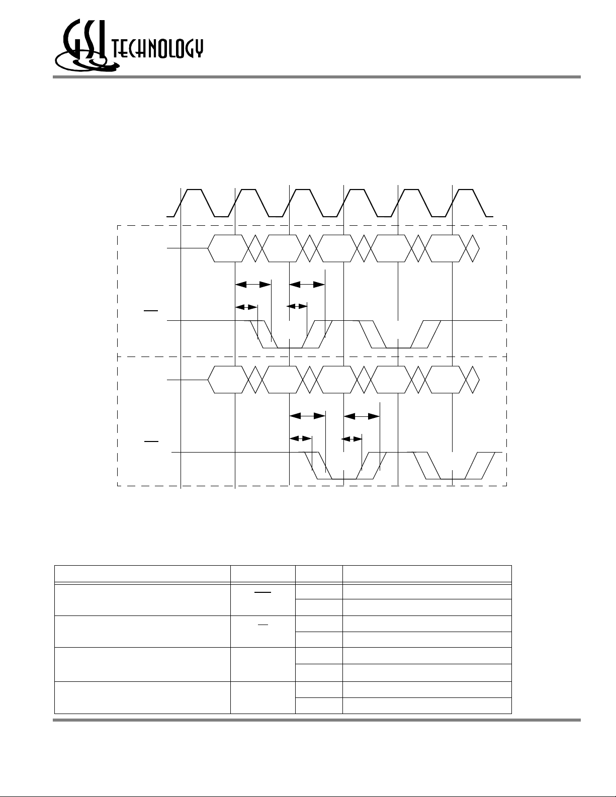
Preliminary
GS88118/36T-11/11.5/100/80/66
This SRAM includes a write data parity check that checks the validity of data coming into the RAM on write cycles. In Flow
Through mode, write data errors are reported in the cycle following the data input cycle. In Pipeline mode, write data errors are
reported one clock cycle later. (See Write Parity Error Output Timing Diagram.) The Data Parity Mode (DP) pin must be tied
high to set the RAM to check for even parity or low to check for odd parity. Read data parity is not checked by the RAM as data.
Validity is best established at the data’s destination. The Parity Error Output is an open drain output and drives low to indicate a
parity error. Multiple Parity Error Output pins may share a common pull-up resistor.
Write Parity Error Output Timing Diagram
CK
Flow Through ModePipelined Mode
Mode Pin Functions
DQ
QE
DQ
QE
D In A D In B D In C D In D D In E
tKQ
tLZ
D In A D In B D In C D In D D In E
Err A
tKQX
tKQ
tLZ
tHZ
Err C
tHZ
tKQX
Err A Err C
BPR 1999.05.18
Mode Name Pin Name State Function
Burst Order Control LBO
Output Register Control FT
Power Down Control ZZ
ByteSafe Data Parity Control DP
Rev: 1.11 9/2000 7/33 © 2000, Giga Semiconductor, Inc.
Specifications cited are subject to change without notice. For latest documentation see http://www.gsitechnology.com.
L Linear Burst
H or NC Interleaved Burst
L Flow Through
H or NC Pipeline
L or NC Active
H
L Check for Odd Parity
H or NC Check for Even Parity
Standby, IDD = I
SB
Page 8
Preliminary
Linear Burst Sequence
I
GS88118/36T-11/11.5/100/80/66
Note:
There are pull-up devices on the LBO, DP and FT pins and a pull down device on the ZZ pin, so those input pins can be unconnected and the
chip will operate in the default states as specified in the above table.
Burst Counter Sequences
nterleaved Burst Sequence
A[1:0] A[1:0] A[1:0] A[1:0]
1st address 00 01 10 11
2nd address 01 10 11 00
3rd address 10 11 00 01
4th address 11 00 01 10
Note: The burst counter wraps to initial state on the 5th clock.
1st address 00 01 10 11
2nd address 01 00 11 10
3rd address 10 11 00 01
4th address 11 10 01 00
Note: The burst counter wraps to initial state on the 5th clock.
A[1:0] A[1:0] A[1:0] A[1:0]
Byte Write Truth Table
Function GW BW BA BB BC BD Notes
Read H H X X X X 1
Read H L H H H H 1
Write byte a H L L H H H 2, 3
Write byte b H L H L H H 2, 3
Write byte c H L H H L H 2, 3, 4
Write byte d H L H H H L 2, 3, 4
Write all bytes H L L L L L 2, 3, 4
BPR 1999.05.18
Write all bytes L X X X X X
Notes:
1. All byte outputs are active in read cycles regardless of the state of Byte Write Enable inputs.
2. Byte Write Enable inputs BA, BB, BC, and/or BD may be used in any combination with BW to write single or multiple bytes.
3. All byte I/Os remain High-Z during all write operations regardless of the state of Byte Write Enable inputs.
4. Bytes “C” and “D” are only available on the x36 version.
Rev: 1.11 9/2000 8/33 © 2000, Giga Semiconductor, Inc.
Specifications cited are subject to change without notice. For latest documentation see http://www.gsitechnology.com.
Page 9
Synchronous Truth Table
Preliminary
GS88118/36T-11/11.5/100/80/66
Operation
Deselect Cycle, Power Down None X H X X L X X High-Z
Deselect Cycle, Power Down None X L F L X X X High-Z
Deselect Cycle, Power Down None X L F H L X X High-Z
Read Cycle, Begin Burst External R L T L X X X Q
Read Cycle, Begin Burst External R L T H L X F Q
Write Cycle, Begin Burst External W L T H L X T D
Read Cycle, Continue Burst Next CR X X H H L F Q
Read Cycle, Continue Burst Next CR H X X H L F Q
Write Cycle, Continue Burst Next CW X X H H L T D
Write Cycle, Continue Burst Next CW H X X H L T D
Read Cycle, Suspend Burst Current X X H H H F Q
Read Cycle, Suspend Burst Current H X X H H F Q
Write Cycle, Suspend Burst Current X X H H H T D
Write Cycle, Suspend Burst Current H X X H H T D
Notes:
1. X = Don’t Care, H = High, L = Low.
2. For x36 Version, E = T (True) if E2 = 1; E = F (False) if E2 = 0.
3. W = T (True) and F (False) is defined in the Byte Write Truth Table preceding.
4. G is an asynchronous input. G can be driven high at any time to disable active output drivers. G low can only enable active drivers (shown
as “Q” in the Truth Table above).
Address
Used
Diagram
5
Key
E1
State
2
E2
(x36only)
ADSP ADSC ADV
W
3
DQ
4
5. All input combinations shown above are tested and supported. Input combinations shown in gray boxes need not be used to accomplish
basic synchronous or synchronous burst operations and may be avoided for simplicity.
6. Tying ADSP high and ADSC low allows simple non-burst synchronous operations. See BOLD items above.
7. Tying ADSP high and ADV low while using ADSC to load new addresses allows simple burst operations. See ITALIC items above.
Rev: 1.11 9/2000 9/33 © 2000, Giga Semiconductor, Inc.
Specifications cited are subject to change without notice. For latest documentation see http://www.gsitechnology.com.
Page 10
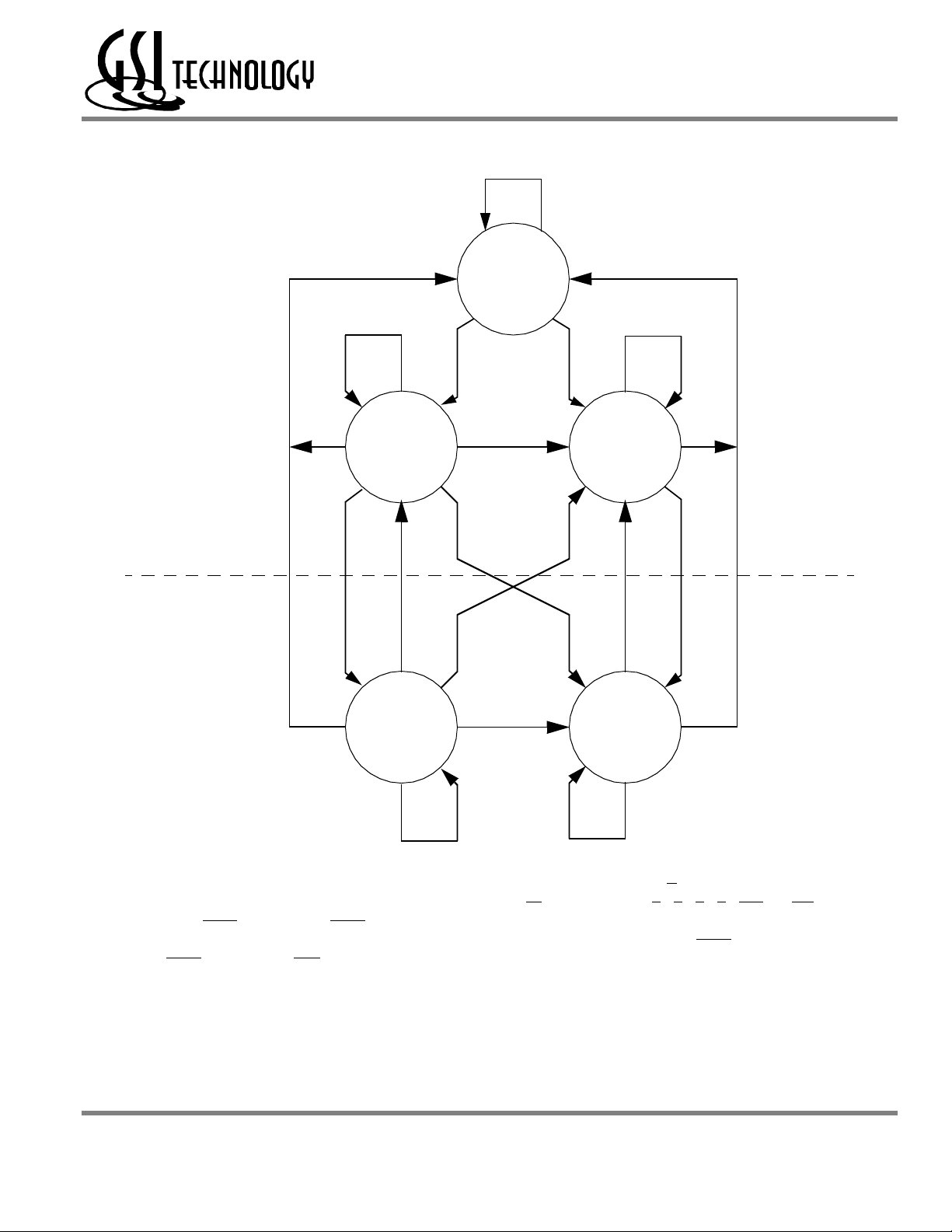
Preliminary
Simplified State Diagram
GS88118/36T-11/11.5/100/80/66
X
Deselect
W R
W
X
Simple Synchronous OperationSimple Burst Synchronous Operation
First Write
W R
Burst Write
CW CR
R
CR
R
CR
R
First Read
Burst Read
X
CRCW
XX
Notes:
1. The diagram shows only supported (tested) synchronous state transitions. The diagram presumes G is tied low.
2. The upper portion of the diagram assumes active use of only the Enable (E1and E2) and Write (BA, BB, BC, BD, BW, and GW) control
inputs, and that ADSP is tied high and ADSC is tied low.
3. The upper and lower portions of the diagram together assume active use of only the Enable, Write, and ADSC control inputs, and
assumes ADSP is tied high and ADV is tied low.
Rev: 1.11 9/2000 10/33 © 2000, Giga Semiconductor, Inc.
Specifications cited are subject to change without notice. For latest documentation see http://www.gsitechnology.com.
Page 11

Simplified State Diagram with G
Preliminary
GS88118/36T-11/11.5/100/80/66
X
Deselect
W R
W
X
First Write
W
X
Burst Write
CW CR
R
CR
R
CR
W
CW
W
CW
R
First Read
R
Burst Read
X
CRCW
X
Notes:
1. The diagram shows supported (tested) synchronous state transitions plus supported transitions that depend upon the use of G.
2. Use of “Dummy Reads” (Read Cycles with G High) may be used to make the transition from Read cycles to Write cycles without passing
through a Deselect cycle. Dummy Read cycles increment the address counter just like normal Read cycles.
3. Transitions shown in grey tone assume G has been pulsed high long enough to turn the RAM’s drivers off and for incoming data to meet
Data Input Set Up Time.
Rev: 1.11 9/2000 11/33 © 2000, Giga Semiconductor, Inc.
Specifications cited are subject to change without notice. For latest documentation see http://www.gsitechnology.com.
Page 12

Preliminary
GS88118/36T-11/11.5/100/80/66
Absolute Maximum Ratings
(All voltages reference to VSS)
Symbol Description Value Unit
V
DD
V
DDQ
V
CK
V
I/O
V
IN
I
IN
I
OUT
P
D
T
STG
T
BIAS
Note:
Permanent damage to the device may occur if the Absolute Maximum Ratings are exceeded. Operation should be restricted to Recommended
Operating Conditions. Exposure to conditions exceeding the Absolute Maximum Ratings, for an extended period of time, may affect reliability of
this component.
Voltage on VDD Pins
Voltage in V
Pins –0.5 to V
DDQ
–0.5 to 4.6 V
DD
V
Voltage on Clock Input Pin –0.5 to 6 V
Voltage on I/O Pins
Voltage on Other Input Pins
–0.5 to V
–0.5 to V
+0.5 (≤ 4.6 V max.)
DDQ
+0.5 (≤ 4.6 V max.)
DD
V
V
Input Current on Any Pin +/–20 mA
Output Current on Any I/O Pin +/–20 mA
Package Power Dissipation 1.5 W
Storage Temperature –55 to 125
Temperature Under Bias –55 to 125
o
o
C
C
Recommended Operating Conditions
Parameter Symbol Min. Typ. Max. Unit Notes
Supply Voltage
I/O Supply Voltage
Input High Voltage
Input Low Voltage
Ambient Temperature (Commercial Range Versions)
Ambient Temperature (Industrial Range Versions)
Notes:
1. Unless otherwise noted, all performance specifications quoted are evaluated for worst case at both 2.75 V ≤ V
(i.e., 2.5 V I/O) and 3.6 V ≤ V
≤ 3.135 V (i.e., 3.3 V I/O), and quoted at whichever condition is worst case.
DDQ
2. This device features input buffers compatible with both 3.3 V and 2.5 V I/O drivers.
3. Most speed grades and configurations of this device are offered in both Commercial and Industrial Temperature ranges. The part number of
Industrial Temperature Range versions end the character “I”. Unless otherwise noted, all performance specifications quoted are evaluated
for worst case in the temperature range marked on the device.
4. Input Under/overshoot voltage must be –2 V > Vi < V
V
DD
V
DDQ
V
IH
V
IL
T
A
T
A
+2 V with a pulse width not to exceed 20% tKC.
DD
3.135 3.3 3.6 V
2.375 2.5
1.7 —
–0.3 — 0.8 V 2
0 25 70 °C 3
–40 25 85 °C 3
V
DD
V
+0.3
DD
V 1
V 2
≤ 2.375 V
DDQ
Rev: 1.11 9/2000 12/33 © 2000, Giga Semiconductor, Inc.
Specifications cited are subject to change without notice. For latest documentation see http://www.gsitechnology.com.
Page 13

GS88118/36T-11/11.5/100/80/66
Undershoot Measurement and Timing Overshoot Measurement and Timing
V
IH
VDD + 2.0 V
V
SS
50%
20% tKC
Preliminary
50%
VSS – 2.0 V
20% tKC
V
DD
V
IL
Capacitance
(TA = 25oC, f = 1 MHZ, V
DD
= 3.3 V)
Parameter Symbol Test conditions Typ. Max. Unit
Input Capacitance
Input/Output Capacitance
Note: These parameters are sample tested.
C
IN
C
I/O
V
V
IN
OUT
= 0 V
= 0 V
4 5 pF
6 7 pF
Package Thermal Characteristics
Rating Layer Board Symbol Max Unit Notes
R
R
R
ΘJA
ΘJA
ΘJC
40 °C/W 1,2
24 °C/W 1,2
9 °C/W 3
Junction to Ambient (at 200 lfm) single
Junction to Ambient (at 200 lfm) four
Junction to Case (TOP) —
Notes:
1. Junction temperature is a function of SRAM power dissipation, package thermal resistance, mounting board temperature, ambient. Temperature air flow, board density, and PCB thermal resistance.
2. SCMI G-38-87
3. Average thermal resistance between die and top surface, MIL SPEC-883, Method 1012.1
Rev: 1.11 9/2000 13/33 © 2000, Giga Semiconductor, Inc.
Specifications cited are subject to change without notice. For latest documentation see http://www.gsitechnology.com.
Page 14

AC Test Conditions
Parameter Conditions
Input high level 2.3 V
Input low level 0.2 V
Input slew rate 1 V/ns
Input reference level 1.25 V
Output reference level 1.25 V
Output load Fig. 1& 2
Notes:
1. Include scope and jig capacitance.
2. Test conditions as specified with output loading as shown in Fig. 1 unless otherwise noted.
3. Output Load 2 for tLZ, tHZ, t
4. Device is deselected as defined by the Truth Table.
DQ
and t
OLZ
Output Load 1
OHZ
Preliminary
GS88118/36T-11/11.5/100/80/66
Output Load 2
2.5 V
DC Electrical Characteristics
Parameter Symbol Test Conditions Min Max
Input Leakage Current
(except mode pins)
ZZ Input Current
Mode Pin Input Current
Output Leakage Current
Output High Voltage
Output High Voltage
Output Low Voltage
I
INZZ
I
INM
I
V
V
V
I
IL
OL
OH
OH
OL
50Ω
VT = 1.25 V
I
OH
I
OH
*
30pF
* Distributed Test Jig Capacitance
V
= 0 to V
IN
V
DD ≥ VIN ≥ VIH
0 V ≤ V
V
DD ≥ VIN ≥ VIL
0 V ≤ V
IN
IN
DD
≤ V
≤ V
IH
IL
Output Disable,
V
= 0 to V
OUT
= –8 mA, V
= –8 mA, V
I
OL
DDQ
DDQ
= 8 mA
DD
= 2.375 V
= 3.135 V
DQ
5pF
–1 uA 1 uA
–1 uA
–1 uA
300 uA
–300 uA
–1 uA
–1 uA 1 uA
1.7 V —
2.4 V —
— 0.4 V
*
1 uA
1 uA
1 uA
225Ω
225Ω
Rev: 1.11 9/2000 14/33 © 2000, Giga Semiconductor, Inc.
Specifications cited are subject to change without notice. For latest documentation see http://www.gsitechnology.com.
Page 15

Operating Currents
Parameter Test Conditions Symbol
Device Selected;
Operating
Current
Standby
Current
Deselect
Current
All other inputs
≥VIH or ≤ V
Output open
ZZ ≥ V
Device Deselected;
All other inputs
≥ VIH or ≤ V
DD
- 0.2V
Pipeline
IL
Flow-Thru
Pipeline
Flow-Thru
Pipeline
IL
Flow-Thru
Preliminary
GS88118/36T-11/11.5/100/80/66
-11 -11.5 -100 -80 -66
0
–40
to
70°C
I
DD
I
DD
I
SB
I
SB
I
DD
I
DD
225 235 225 235 225 235 200 210 185 195 mA
180 190 180 190 180 190 175 185 165 175 mA
30 40 30 40 30 40 30 40 30 40 mA
30 40 30 40 30 40 30 40 30 40 mA
80 90 80 90 80 90 70 80 60 70 mA
65 75 65 75 65 75 55 65 50 60 mA
to
85°C
0
to
70°C
–40
to
85°C
0
to
70°C
–40
to
85°C
0
to
70°C
–40
to
85°C
0
to
70°C
–40
to
85°C
Unit
Rev: 1.11 9/2000 15/33 © 2000, Giga Semiconductor, Inc.
Specifications cited are subject to change without notice. For latest documentation see http://www.gsitechnology.com.
Page 16

AC Electrical Characteristics
Preliminary
GS88118/36T-11/11.5/100/80/66
Pipeline
Flow-
Thru
Parameter Symbol
-11 -11.5 -100 -80 -66
Min Max Min Max Min Max Min Max Min Max
Clock Cycle Time tKC 10 — 10 — 10 — 12.5 — 15 — ns
Clock to Output Valid tKQ — 4.0 — 4.0 — 4.0 — 4.5 — 5 ns
Clock to Output Invalid tKQX 1.5 — 1.5 — 1.5 — 1.5 — 1.5 — ns
Clock to Output in Low-Z
tLZ
1
1.5 — 1.5 — 1.5 — 1.5 — 1.5 — ns
Clock Cycle Time tKC 15.0 — 15.0 — 15.0 — 15.0 — 20 — ns
Clock to Output Valid tKQ — 11.0 — 11.5 — 12.0 — 14.0 — 18 ns
Clock to Output Invalid tKQX 3.0 — 3.0 — 3.0 — 3.0 — 3.0 — ns
Clock to Output in Low-Z
tLZ
1
3.0 — 3.0 — 3.0 — 3.0 — 3.0 — ns
Clock HIGH Time tKH 1.7 — 1.7 — 2 — 2 — 2.3 — ns
Clock LOW Time tKL 2 — 2 — 2.2 — 2.2 — 2.5 — ns
Clock to Output in High-Z
tHZ
1
1.5 4.0 1.5 4.2 1.5 4.5 1.5 4.5 1.5 4.8 ns
G to Output Valid tOE — 4.0 — 4.2 — 4.5 — 4.5 — 4.8 ns
G to output in Low-Z
G to output in High-Z
tOLZ
tOHZ
1
1
0 — 0 — 0 — 0 — 0 — ns
— 4.0 — 4.2 — 4.5 — 4.5 — 4.8 ns
Setup time tS 1.5 — 2.0 — 2.0 — 2.0 — 2.0 — ns
Hold time tH 0.5 — 0.5 — 0.5 — 0.5 — 0.5 — ns
ZZ setup time
ZZ hold time
tZZS
tZZH
2
2
5 — 5 — 5 — 5 — 5 — ns
1 — 1 — 1 — 1 — 1 — ns
ZZ recovery tZZR 20 — 20 — 20 — 20 — 20 — ns
Unit
Notes:
1. These parameters are sampled and are not 100% tested.
2. ZZ is an asynchronous signal. However, in order to be recognized on any given clock cycle, ZZ must meet the specified setup and hold
times as specified above.
Rev: 1.11 9/2000 16/33 © 2000, Giga Semiconductor, Inc.
Specifications cited are subject to change without notice. For latest documentation see http://www.gsitechnology.com.
Page 17

Write Cycle Timing
Preliminary
GS88118/36T-11/11.5/100/80/66
CK
ADSP
ADSC
ADV
A0–An
GW
BW
Single Write
tH
tS
tH
tS
WR1
Burst Write
ADSP is blocked by E inactive
tKC
tKL
tKH
tH
tS
tH
tS
ADV must be inactive for ADSP Write
WR2 WR3
tS tH
tH
tS
tS
tH
Write
ADSC initiated write
Deselected
BA–BD
tS
WR1 WR2 WR3
WR1
tH
WR2 WR3
E1 masks ADSP
E1
tS
tH
Deselected with E2
E2
E2 only sampled with ADSP or ADSC
G
tS
tH
DQA–DQD
Hi-Z
D1A
Rev: 1.11 9/2000 17/33 © 2000, Giga Semiconductor, Inc.
Specifications cited are subject to change without notice. For latest documentation see http://www.gsitechnology.com.
Write specified byte for 2A and all bytes for 2B, 2C& 2D
D2A D2B
D2C D2D D3A
Page 18

Preliminary
Flow Through Read Cycle Timing
GS88118/36T-11/11.5/100/80/66
CK
ADSP
ADSC
ADV
A0–An
GW
BW
Single Read
tS
tH
tS
tS
tH
RD1
tS
tS
tKL
tKH
tS tH
tH
RD2 RD3
Burst Read
ADSP is blocked by E inactive
tKC
Suspend Burst
ADSC initiated read
Suspend Burst
tH
tH
BA–BD
tH
tS
E1 masks ADSP
E1
tH
tS
E2 only sampled with ADSP or ADSC
Deselected with E2
E2
tOE
tOHZ
G
Q2A
tKQX
Q2cQ2B
Q2D
tOLZ
DQA–DQD
Rev: 1.11 9/2000 18/33 © 2000, Giga Semiconductor, Inc.
Specifications cited are subject to change without notice. For latest documentation see http://www.gsitechnology.com.
Hi-Z
tLZ
tKQ
Q1A
tKQX
Q3A
tHZ
Page 19

Flow Through Read-Write Cycle Timing
Preliminary
GS88118/36T-11/11.5/100/80/66
CK
ADSP
ADSC
ADV
A0–An
GW
BW
tKL
Single Write
tKC
tH
tS
Single Read
tH
tS
tS tH
tS
tH
RD1 WR1
tS tH
tS
tKH
tS tH
tH
Burst Read
ADSP is blocked by E inactive
ADSC initiated read
RD2
DQA–DQD
BA–BD
E1
E2
G
Hi-Z
tS
tS
tH
tH
tKQ
E2 only sampled with ADSP and ADSC
tOE
tOHZ
Q1A D1A
tS
WR1
tH
E1 masks ADSP
Q2A
Burst wrap around to it’s initial state
Q2B Q2c
Q2D
Q2A
Rev: 1.11 9/2000 19/33 © 2000, Giga Semiconductor, Inc.
Specifications cited are subject to change without notice. For latest documentation see http://www.gsitechnology.com.
Page 20

Pipelined SCD Read-Write Cycle Timing
Preliminary
GS88118/36T-11/11.5/100/80/66
CK
ADSP
ADSC
ADV
A0–An
GW
BW
tKL
Single Write
tKC
tS tH
tH
tS
ADSP is blocked by E inactive
ADSC initiated read
RD2
Single Read Burst Read
tH
tS
tH
tS
tS
tH
RD1 WR1
tS
tH
tS tH
tKH
BWA–BWD
tS
tH
WR1
E1 masks ADSP
E1
tS tH
E2 only sampled with ADSP and ADSC
E2
tOE tOHZ
G
tS
DQA–DQD
Hi-Z
tKQ
Q1A
Rev: 1.11 9/2000 20/33 © 2000, Giga Semiconductor, Inc.
Specifications cited are subject to change without notice. For latest documentation see http://www.gsitechnology.com.
tH
D1A Q2A
Q2B Q2c
Q2D
Page 21

Preliminary
Pipelined SCD Read Cycle Timing
GS88118/36T-11/11.5/100/80/66
CK
ADSP
ADSC
ADV
A0–An
GW
BW
Single Read
tH
tS
tS
tH
tS
RD1
tS
tS
tH
tS
RD2
tKH
tH
tKL
Burst Read
tKC
ADSP is blocked by E inactive
ADSC initiated read
Suspend Burst
RD3
tH
tH
BWA–BWD
tH
tS
E1 masks ADSP
E1
tH
tS
E2 only sampled with ADSP or ADSC
Deselected with E2
E2
tOE
G
tOHZ
tKQX
Q2A
Q2B
Q2c
DQA–DQD
Hi-Z
tOLZ
Q1A
tLZ
tKQ
Rev: 1.11 9/2000 21/33 © 2000, Giga Semiconductor, Inc.
Specifications cited are subject to change without notice. For latest documentation see http://www.gsitechnology.com.
tKQX
Q3AQ2D
tHZ
Page 22

Sleep Mode Timing Diagram
CK
tS
ADSP
ADSC
ZZ
Application Tips
tH
tKC
tKH
tKL
tZZS
~
~
~
~
~
~
~
~
~
~
~
~
Snooze
tZZH
Preliminary
GS88118/36T-11/11.5/100/80/66
tZZR
Single and Dual Cycle Deselect
SCD devices force the use of “dummy read cycles” (read cycles that are launched normally but that are ended with the output
drivers inactive) in a fully synchronous environment. Dummy read cycles waste performance but their use usually assures there
will be no bus contention in transitions from reads to writes or between banks of RAMs. DCD SRAMs do not waste bandwidth on
dummy cycles and are logically simpler to manage in a multiple bank application (wait states need not be inserted at bank address
boundary crossings) but greater care must be exercised to avoid excessive bus contention.
JTAG Port Operation
Overview
The JTAG Port on this RAM operates in a manner consistent with IEEE Standard 1149.1-1990, a serial boundary scan interface
standard (commonly referred to as JTAG), but does not implement all of the functions required for 1149.1 compliance. Some
functions have been modified or eliminated because they can slow the RAM. Nevertheless, the RAM supports 1149.1-1990 TAP
(Test Access Port) Controller architecture, and can be expected to function in a manner that does not conflict with the operation of
Standard 1149.1 compliant devices. The JTAG Port interfaces with conventional TTL / CMOS logic level signaling.
Disabling the JTAG Port
It is possible to use this device without utilizing the JTAG port. The port is reset at power-up and will remain inactive unless
clocked. TCK, TDI, and TMS are designed with internal pull-up circuits. To assure normal operation of the RAM with the JTAG
Port unused, TCK, TDI, and TMS may be left floating or tied to either VDD or VSS. TDO should be left unconnected.
Rev: 1.11 9/2000 22/33 © 2000, Giga Semiconductor, Inc.
Specifications cited are subject to change without notice. For latest documentation see http://www.gsitechnology.com.
Page 23

Preliminary
GS88118/36T-11/11.5/100/80/66
JTAG Pin Descriptions
Pin Pin Name I/O Description
TCK Test Clock In
TMS
TDI Test Data In In
TDO Test Data Out Out
Note:
This device does not have a TRST (TAP Reset) pin. TRST is optional in IEEE 1149.1. The Test-Logic-Reset state is entered while TMS is
held high for five rising edges of TCK. The TAP Controller is also reset automaticly at power-up.
Test Mode
Select
JTAG Port Registers
Clocks all TAP events. All inputs are captured on the rising edge of TCK and all outputs propagate from the
falling edge of TCK.
The TMS input is sampled on the rising edge of TCK. This is the command input for the TAP controller state
In
machine. An undriven TMS input will produce the same result as a logic one input level.
The TDI input is sampled on the rising edge of TCK. This is the input side of the serial registers placed
between TDI and TDO. The register placed between TDI and TDO is determined by the state of the TAP
Controller state machine and the instruction that is currently loaded in the TAP Instruction Register (refer to
the TAP Controller State Diagram). An undriven TDI pin will produce the same result as a logic one input
level.
Output that is active depending on the state of the TAP state machine. Output changes in response to the
falling edge of TCK. This is the output side of the serial registers placed between TDI and TDO.
Overview
The various JTAG registers, refered to as TAP Registers, are selected (one at a time) via the sequences of 1s and 0s applied to TMS
as TCK is strobed. Each of the TAP Registers are serial shift registers that capture serial input data on the rising edge of TCK and
push serial data out on the next falling edge of TCK. When a register is selected it is placed between the TDI and TDO pins.
Instruction Register
The Instruction Register holds the instructions that are executed by the TAP controller when it is moved into the Run, Test/Idle or
the various data register states. Instructions are 3 bits long. The Instruction Register can be loaded when it is placed between the
TDI and TDO pins. The Instruction Register is automatically preloaded with the IDCODE instruction at power-up or whenever the
controller is placed in Test-Logic-Reset state.
Bypass Register
The Bypass Register is a single-bit register that can be placed between TDI and TDO. It allows serial test data to be passed through
the RAMs JTAG Port to another device in the scan chain with as little delay as possible.
Boundary Scan Register
Boundary Scan Register is a collection of flip flops that can be preset by the logic level found on the RAM’s input or I/O pins. The
flip flops are then daisy chained together so the levels found can be shifted serially out of the JTAG Port’s TDO pin. The
Boundary Scan Register also includes a number of place holder flip flops (always set to a logic 1). The relationship between the
device pins and the bits in the Boundary Scan Register is described in the Scan Order Table following. The Boundary Scan
Register, under the control of the TAP Controller, is loaded with the contents of the RAMs I/O ring when the controller is in
Capture-DR state and then is placed between the TDI and TDO pins when the controller is moved to Shift-DR state. Two TAP
instructions can be used to activate the Boundary Scan Register.
Rev: 1.11 9/2000 23/33 © 2000, Giga Semiconductor, Inc.
Specifications cited are subject to change without notice. For latest documentation see http://www.gsitechnology.com.
Page 24

Preliminary
GS88118/36T-11/11.5/100/80/66
JTAG TAP Block Diagram
0
Bypass Register
012
Instruction Register
TDI
ID Code Register
31 30 29
· · · ·
012
Boundary Scan Register
n
· · ·· · ·· · ·
012
TMS
TCK
Test Access Port (TAP) Controller
Identification (ID) Register
The ID Register is a 32-bit register that is loaded with a device and vendor specific 32-bit code when the controller is put in
Capture-DR state with the IDCODE command loaded in the Instruction Register. The code is loaded from a 32-bit on-chip ROM.
It describes various attributes of the RAM as indicated below. The register is then placed between the TDI and TDO pins when the
controller is moved into Shift-DR state. Bit 0 in the register is the LSB and the first to reach TDO when shifting begins.
ID Register Contents
TDO
Die
Revision
Code
Not Used
I/O
Configuration
GSI Technology
JEDEC Vendor
ID Code
Presence Register
Bit # 31 30 29 28 27 26 25 24 23 22 21 20 19 18 17 16 15 14 13 12
x36
X X X X 0 0 0 0 0 0 0 0 0 0 0 0 0 0 0 1 0 0 0 1 1 0 1 1 0 0 1 1
x18
X X X X 0 0 0 0 0 0 0 0 0 0 0 0 0 0 1 1 0 0 0 1 1 0 1 1 0 0 1 1
1
10 9 8 7 6 5 4 3 2 1 0
1
Tap Controller Instruction Set
Overview
There are two classes of instructions defined in the Standard 1149.1-1990; the standard (Public) instructions, and device specific
(Private) instructions. Some Public instructions, are mandatory for 1149.1 compliance. Optional Public instructions must be
implemented in prescribed ways. Although the TAP controller in this device follows the 1149.1 conventions, it is not 1194.1compliant because some of the mandatory instructions are not fully implemented. The TAP on this device may be used to monitor
all input and I/O pads, but cannot be used to load address, data or control signals into the RAM or to preload the I/O buffers.This
device will not perform EXTEST, INTEST or the SAMPLE/PRELOAD command.
When the TAP controller is placed in Capture-IR state the two least significant bits of the instruction register are loaded with 01.
When the controller is moved to the Shift-IR state the Instruction Register is placed between TDI and TDO. In this state the desired
Rev: 1.11 9/2000 24/33 © 2000, Giga Semiconductor, Inc.
Specifications cited are subject to change without notice. For latest documentation see http://www.gsitechnology.com.
Page 25

Preliminary
GS88118/36T-11/11.5/100/80/66
instruction is serially loaded through the TDI input (while the previous contents are shifted out at TDO). For all instructions, the
TAP executes newly loaded instructions only when the controller is moved to Update-IR state. The TAP instruction set for this
device is listed in the following table.
JTAG Tap Controller State Diagram
Test Logic Reset
1
0
Run Test Idle
0
1 1 1
Select DR
1
Capture DR
Shift DR
1
Exit1 DR
Pause DR
Exit2 DR
Update DR
1
Select IR
0
1
0
0
Capture IR
0
Shift IR
1
0
0
1
1
Exit1 IR
0
Pause IR
1
1
0
0 0
1
Exit2 IR
1
Update IR
0
1 0
0
0
Instruction Descriptions
BYPASS
When the BYPASS instruction is loaded in the Instruction Register the Bypass Register is placed between TDI and TDO. This occurs when
the TAP controller is moved to the Shift-DR state. This allows the board level scan path to be shortened to facilitate testing of other devices
in the scan path.
SAMPLE/PRELOAD
SAMPLE/PRELOAD is a Standard 1149.1 mandatory public instruction. When the SAMPLE/PRELOAD instruction is loaded in the Instruction Register, moving the TAP controller into the Capture-DR state loads the data in the RAMs input and I/O buffers into the Boundary Scan
Register. Because the RAM clock is independent from the TAP Clock (TCK) it is possible for the TAP to attempt to capture the I/O ring contents while the input buffers are in transition (i.e. in a metastable state). Although allowing the TAP to sample metastable inputs will not harm
the device, repeatable results cannot be expected. RAM input signals must be stabilized for long enough to meet the TAPs input data capture set-up plus hold time (tTS plus tTH ). The RAMs clock inputs need not be paused for any other TAP operation except capturing the I/O
ring contents into the Boundary Scan Register. Moving the controller to Shift-DR state then places the boundary scan register between the
TDI and TDO pins. Because the PRELOAD portion of the command is not implemented in this device, moving the controller to the UpdateDR state with the SAMPLE / PRELOAD instruction loaded in the Instruction Register has the same effect as the Pause-DR command. This
functionality is not Standard 1149.1-compliant.
Rev: 1.11 9/2000 25/33 © 2000, Giga Semiconductor, Inc.
Specifications cited are subject to change without notice. For latest documentation see http://www.gsitechnology.com.
Page 26

Preliminary
GS88118/36T-11/11.5/100/80/66
EXTEST
EXTEST is an IEEE 1149.1 mandatory public instruction. It is to be executed whenever the instruction register, whatever length it may be in
the device, is loaded with all logic 0s. EXTEST is not implemented in this device. Therefore, this device is not 1149.1-compliant. Nevertheless, this RAM’s TAP does respond to an all zeros instruction, as follows. With the EXTEST (000) instruction loaded in the instruction register the RAM responds just as it does in response to the BYPASS instruction described above.
IDCODE
The IDCODE instruction causes the ID ROM to be loaded into the ID register when the controller is in Capture-DR mode and places the ID
register between the TDI and TDO pins in Shift-DR mode. The IDCODE instruction is the default instruction loaded in at power up and any
time the controller is placed in the Test-Logic-Reset state.
SAMPLE-Z
If the SAMPLE-Z instruction is loaded in the instruction register, all RAM outputs are forced to an inactive drive state (high-Z) and the
Boundary Scan Register is connected between TDI and TDO when the TAP controller is moved to the Shift-DR state.
RFU
These instructions are Reserved for Future Use. In this device they replicate the BYPASS instruction.
JTAG TAP Instruction Set Summary
Instruction Code Description Notes
EXTEST 000
IDCODE 001 Preloads ID Register and places it between TDI and TDO. 1, 2
SAMPLE-Z 010
RFU 011
SAMPLE/
PRELOAD
GSI 101 GSI private instruction. 1
RFU 110
BYPASS 111 Places Bypass Register between TDI and TDO. 1
Notes:
1. Instruction codes expressed in binary, MSB on left, LSB on right.
2. Default instruction automatically loaded at power-up and in test-logic-reset state.
100
Replicates BYPASS instruction. Places Bypass Register between TDI and TDO.
This RAM does not implement 1149.1 EXTEST function. *Not 1149.1 Compliant *
Captures I/O ring contents. Places the Boundary Scan Register between TDI and TDO.
Forces all RAM output drivers to High-Z.
Do not use this instruction; Reserved for Future Use.
Replicates BYPASS instruction. Places Bypass Register between TDI and TDO.
Captures I/O ring contents. Places the Boundary Scan Register between TDI and TDO.
This RAM does not implement 1149.1 PRELOAD function. *Not 1149.1 Compliant *
Do not use this instruction; Reserved for Future Use.
Replicates BYPASS instruction. Places Bypass Register between TDI and TDO.
1
1
1
1
1
Rev: 1.11 9/2000 26/33 © 2000, Giga Semiconductor, Inc.
Specifications cited are subject to change without notice. For latest documentation see http://www.gsitechnology.com.
Page 27

JTAG Port Recommended Operating Conditions and DC Characteristics
Parameter Symbol Min. Max. Unit Notes
Test Port Input High Voltage
Test Port Input Low Voltage
TMS, TCK and TDI Input Leakage Current
TMS, TCK and TDI Input Leakage Current
TDO Output Leakage Current
Test Port Output High Voltage
Test Port Output Low Voltage
V
V
I
INTH
I
INTL
I
OLT
V
V
IHT
ILT
–300 1 uA 3
OHT
OLT
Notes:
1. This device features input buffers compatible with both 3.3 V and 2.5 V I/O drivers.
2. Input Under/overshoot voltage must be –2 V > Vi < V
+2 V with a pulse width not to exceed 20%
DD
tTKC.
3. V
DD ≥ VIN ≥ VIL
4. 0 V ≤ V
5. Output Disable, V
IN
≤ V
IL
OUT
= 0 to V
DD
6. The TDO output driver is served by the VDD supply.
7. I
8. I
OH
= +4 mA
OL
= –4 mA
V
1.7
DD
+0.3
–0.3 0.8 V 1, 2
–1 1 uA 4
–1 1 uA 5
2.4 — V 6, 7
— 0.4 V 6, 8
Preliminary
GS88118/36T-11/11.5/100/80/66
V 1, 2
JTAG Port AC Test Conditions
Parameter Conditions
Input high level 2.3 V
Input low level 0.2 V
Input slew rate 1 V/ns
Input reference level 1.25 V
Output reference level 1.25 V
Notes:
1. Include scope and jig capacitance.
DQ
JTAG Port AC Test Load
50Ω
VT = 1.25 V
* Distributed Test Jig Capacitance
30pF
*
Rev: 1.11 9/2000 27/33 © 2000, Giga Semiconductor, Inc.
Specifications cited are subject to change without notice. For latest documentation see http://www.gsitechnology.com.
Page 28

JTAG Port Timing Diagram
Preliminary
GS88118/36T-11/11.5/100/80/66
tTKH
tTKL
tTKC
TCK
tTS tTH
TMS
TDI
TDO
tTKQ
JTAG Port AC Electrical Characteristics
Parameter Symbol Min Max Unit
TCK Cycle Time tTKC 20 — ns
TCK Low to TDO Valid tTKQ — 10 ns
TCK High Pulse Width tTKH 10 — ns
TCK Low Pulse Width tTKL 10 — ns
TDI & TMS Set Up Time tTS 5 — ns
TDI & TMS Hold Time tTH 5 — ns
Rev: 1.11 9/2000 28/33 © 2000, Giga Semiconductor, Inc.
Specifications cited are subject to change without notice. For latest documentation see http://www.gsitechnology.com.
Page 29

GS88118/36T TQFP Boundary Scan Register
Preliminary
GS88118/36T-11/11.5/100/80/66
Order x36 x18 Pin
1 PH = 0 n/a
2 PH = 0 n/a
3 A10 44
4 A11 45
5 A12 46
6 A13 47
7 A14 48
8 A15 49
9 A16 50
10 x36 = DQA9 NC = 1 51
11 DQA8 NC = 1 52
12 DQA7 NC = 1 53
13 DQA6 NC = 1 56
14 DQA5 NC = 1 57
15 DQA4 DQA1 58
16 DQA3 DQA2 59
17 DQA2 DQA3 62
18 DQA1 DQA4 63
19 ZZ 64
20 QE 66
21 DQB1 DQA5 68
22 DQB2 DQA6 69
23 DQB3 DQA7 72
24 DQB4 DQA8 73
25 DQB5 DQA9 74
26 DQB6 NC = 1 75
27 DQB7 NC = 1 78
28 DQB8 NC = 1 79
29 x36 = DQB9 A18 80
Order x36 x18 Pin
30 A9 81
31 A8 82
32 ADV 83
33 ADSP 84
34 ADSC 85
35 G 86
36 BW 87
37 GW 88
38 CK 89
39 PH = 0 n/a
40 PH = 0 n/a
41 A17 92
42 BA 93
43 BB 94
44 BC NC = 1 95
45 BD NC = 1 96
46 E2 97
47 E1 98
48 A7 99
49 A6 100
50 x36 = DQC9 NC = 1 1
51 DQC8 NC = 1 2
52 DQC7 NC = 1 3
53 DQC6 NC = 1 6
54 DQC5 NC = 1 7
55 DQC4 DQB1 8
56 DQC3 DQB2 9
57 DQC2 DQB3 12
58 DQC1 DQB4 13
Order x36 x18 Pin
59 FT 14
60 DP 16
61 PH = 1 n/a
62 DQD1 DQB5 18
63 DQD2 DQB6 19
64 DQD3 DQB7 22
65 DQD4 DQB8 23
66 DQD5 DQB9 24
67 DQD6 NC = 1 25
68 DQD7 NC = 1 28
69 DQD8 NC = 1 29
70 x36 = DQD9 NC = 1 30
71 LBO 31
72 A5 32
73 A4 33
74 A3 34
75 A2 35
76 A1 36
77 A0 37
78 PH = 0 n/a
BPR 1999.08.11
Notes:
1. The Boundary Scan Register contains a number of registers that are not connected to any pin. They default to the value shown at reset.
2. Registers are listed in exit order (i.e. Location 1 is the first out of the TDO pin.
3. NC = No Connect, NA = Not Active, PH = Place Holder (No associated pin)
Rev: 1.11 9/2000 29/33 © 2000, Giga Semiconductor, Inc.
Specifications cited are subject to change without notice. For latest documentation see http://www.gsitechnology.com.
Page 30

Output Driver Characteristics
I Out (mA)
120.0
100.0
Pull Down Drivers
80.0
60.0
40.0
Preliminary
GS88118/36T-11/11.5/100/80/66
20.0
VDDQ
I Out
0.0
VOut
-20.0
VSS
-40.0
-60.0
Pull Up Drivers
-80.0
-100.0
-120.0
-140.0
-0.5 0 0.5 1 1.5 2 2.5 3 3.5 4
V Out (Pull Down)
VDDQ - V Out (Pull Up)
3.6V PD HD 3.3V PD HD 3.1V PD HD 3.1V PU HD 3.3V PU HD 3.6V PU HD
BPR 1999.05.18
Rev: 1.11 9/2000 30/33 © 2000, Giga Semiconductor, Inc.
Specifications cited are subject to change without notice. For latest documentation see http://www.gsitechnology.com.
Page 31

TQFP Package Drawing
D
Preliminary
GS88118/36T-11/11.5/100/80/66
Symbol Description Min. Nom. Max
A1 Standoff 0.05 0.10 0.15
A2 Body Thickness 1.35 1.40 1.45
b Lead Width 0.20 0.30 0.40
c Lead Thickness 0.09 — 0.20
D Terminal Dimension 21.9 22.0 22.1
D1 Package Body 19.9 20.0 20.1
E Terminal Dimension 15.9 16.0 16.1
E1 Package Body 13.9 14.0 14.1
e Lead Pitch — 0.65 —
L Foot Length 0.45 0.60 0.75
L1 Lead Length — 1.00 —
Y Coplanarity — — 0.10
θ Lead Angle 0° — 7°
L1
A1
θ
L
c
Pin 1
e
D1
b
A2
Y
E1
E
Notes:
1. All dimensions are in millimeters (mm).
2. Package width and length do not include mold protrusion.
BPR 1999.05.18
Rev: 1.11 9/2000 31/33 © 2000, Giga Semiconductor, Inc.
Specifications cited are subject to change without notice. For latest documentation see http://www.gsitechnology.com.
Page 32

Preliminary
GS88118/36T-11/11.5/100/80/66
Ordering Information for GSI Synchronous Burst RAMs
2
Org
514K x 18 GS88118T-11 ByteSafe Pipeline/Flow Through TQFP 100/11 C
514K x 18 GS88118T-11.5 ByteSafe Pipeline/Flow Through TQFP 100/11.5 C
514K x 18 GS88118T-100 ByteSafe Pipeline/Flow Through TQFP 100/12 C
514K x 18 GS88118T-80 ByteSafe Pipeline/Flow Through TQFP 80/14 C
514K x 18 GS88118T-66 ByteSafe Pipeline/Flow Through TQFP 66/18 C
256K x 36 GS88136T-11 ByteSafe Pipeline/Flow Through TQFP 100/11 C
256K x 36 GS88136T-11.5 ByteSafe Pipeline/Flow Through TQFP 100/11.5 C
256K x 36 GS88136T-100 ByteSafe Pipeline/Flow Through TQFP 100/12 C
256K x 36 GS88136T-80 ByteSafe Pipeline/Flow Through TQFP 80/14 C
256K x 36 GS88136T-66 ByteSafe Pipeline/Flow Through TQFP 66/18 C
514K x 18 GS88118T-11I ByteSafe Pipeline/Flow Through TQFP 100/11 I
514K x 18 GS88118T-11.5I ByteSafe Pipeline/Flow Through TQFP 100/11.5 I
514K x 18 GS88118T-100I ByteSafe Pipeline/Flow Through TQFP 100/12 I
514K x 18 GS88118T-80I ByteSafe Pipeline/Flow Through TQFP 80/14 I
514K x 18 GS88118T-66I ByteSafe Pipeline/Flow Through TQFP 66/18 I
256K x 36 GS88136T-11I ByteSafe Pipeline/Flow Through TQFP 100/11 I
256K x 36 GS88136T-11.5I ByteSafe Pipeline/Flow Through TQFP 100/11.5 I
256K x 36 GS88136T-100I ByteSafe Pipeline/Flow Through TQFP 100/12 I
256K x 36 GS88136T-80I ByteSafe Pipeline/Flow Through TQFP 80/14 I
256K x 36 GS88136T-66I ByteSafe Pipeline/Flow Through TQFP 66/18 I
Notes:
1. Customers requiring delivery in Tape and Reel should add the character “T” to the end of the part number. Example: GS88118TT.
2. The speed column indicates the cycle frequency (MHz) of the device in Pipeline mode and the latency (ns) in Flow Through mode. Each
device is Pipeline/Flow Through mode-selectable by the user.
3. TA = C = Commercial Temperature Range. TA = I = Industrial Temperature Range.
4. GSI offers other versions this type of device in many different configurations and with a variety of different features, only some of which
are covered in this data sheet. See the GSI Technology web site (www.gsitechnology.com) for a complete listing of current offerings.
Part Number
1
Type Package
Speed
(MHz/ns)
3
T
A
Status
Rev: 1.11 9/2000 32/33 © 2000, Giga Semiconductor, Inc.
Specifications cited are subject to change without notice. For latest documentation see http://www.gsitechnology.com.
Page 33

Revision History
Preliminary
GS88118/36T-11/11.5/100/80/66
DS/DateRev. Code: Old;
New
GS88118/36TRev1.04h 5/
1999;
1.05 9/1999I
GS88118/36T1.05 9/
1999I;1.06 11/1999J
GS88118/36T1.06 11/
1999J;1.06 11/1999K
GS88118/36T1.06 11/
1999K88118/36T1.07 1/
2000L
GS88118/36T1.07 1/2000M;
GS88118/36T1.08 3/2000N;
Types of Changes
Format or Content
Format/Typos
Content
Content
content
Content
Content
Page;Revisions;Reason
• Last Page/Fixed “GSGS..” in Ordering Information Note.
• Fromatted Pin Outs and Pin Description to new small caps.
• Formatted Block diagrams to new small caps.
• Formatted Timing Diagrams to new small caps.
• Changed “Flow thru” to “Flow Through” in Timing Diagrams.
• Boundary Scan Register/Formatted to new small caps.
• Package Diagram/Changed “Dimesion” to “Dimension”.
• 5/Fixed pin description table to match pinouts.
• Pin Description/Changed chip enables to match pins.
• Pin Description/Changed pin 80 from NC to Address Input.
• Pin Description/Rearranged Address Inputs to match order of
Pinout
• Package Diagram/Changed Dimension D Max from 20.1 to
22.1
• Took out wrong Pinout on page 2 (256K x 32).
• First Release of 880 F.
• Changed Bump 3C to 4L on first page to correspond SCD pin
in BGA pinout.
• Changed order of TQFP Address Inputs to match pinout.
• Changed order of TQFP DATA Input and Output pins to
match pinout.
• New GSI Logo.
• Changed all speed bin information (headings, references,
tables, ordering info..) to reflect 150 - 80Mhz
GS88118/36T1.08 3/2000N;
GS88118/36T1.09 3/2000O;
8818 NGS88118/36T1.09 3/
2000O;
8811836_r1_10
88118_r1_10; 88118_r1_11 Content
Rev: 1.11 9/2000 33/33 © 2000, Giga Semiconductor, Inc.
Specifications cited are subject to change without notice. For latest documentation see http://www.gsitechnology.com.
Content
Content/Format
• Corrections to AC Electrical Characteristics Table -
• Fixed Boundary Scan Register Added Pin 29
• Removed 150 MHz speed bin
• Changed 133 MHz and 117 MHz speed bins to 11 ns and
11.5 ns (100 MHz) numbers
• Updated format to comply with Technical Publications
standards
• Updated Capitance table—removed Input row and changed
Output row to I/O
 Loading...